Determination of the electronics transfer function for current transient measurements
Abstract
We describe a straight-forward method for determining the transfer function of the readout of a sensor for the situation in which the current transient of the sensor can be precisely simulated. The method relies on the convolution theorem of Fourier transforms. The specific example is a planar silicon pad diode. The charge carriers in the sensor are produced by picosecond lasers with light of wavelengths of 675 and 1060 nm. The transfer function is determined from the 1060 nm data with the pad diode biased at 1000 V. It is shown that the simulated sensor response convoluted with this transfer function provides an excellent description of the measured transients for laser light of both wavelengths. The method has been applied successfully for the simulation of current transients of several different silicon pad diodes. It can also be applied for the analysis of transient-current measurements of radiation-damaged solid state sensors, as long as sensors properties, like high-frequency capacitance, are not too different.
keywords:
silicon pad sensor , transient current technique , transfer function , Fourier transformIntroduction
The analysis of current transients from different sensors is frequently limited by the knowledge of the electronics response, which is also influenced by the sensor properties. Examples for silicon sensors are the determination of the electric fields, carrier lifetimes and charge multiplication in radiation-damaged sensors using the Transient Current Technique (TCT, edge-TCT) [1, 2, 3] or charged particles with shallow incident angles [4]. The aim of this Technical Note is to demonstrate that, for an experiment in which the pulse shape from the sensor can be precisely simulated, the electronics transfer function can be obtained from the measured transient using the convolution theorem of Fourier transforms. This transfer function can then be used for analyzing data for which the pulse shape of the sensor is not known. An example is the analysis of measured transients from a radiation-damaged sensor using the known transfer function obtained from the sensor before irradiation, as long as detector properties, like the high-frequency capacitance, do not change too much with irradiation.
Measurement set-up
The measurement set-up used is described in detail in [5, 6, 7]. The measurements have been performed on and pad diodes with different doping, thicknesses of m and m, and 4.4 mm2 and 25 mm2 area. In all cases the electronics response function has been successfully determined. Here we present the results from a pad diode produced by Hamamatsu [8] on a crystal with 204.5 m mechanical thickness, 4.4 mm2 area, and cm-3 phosphorous doping, which was connected by a 3 m long RG58 cable and a bias-T to an amplifier [9], and read out by a Tektronix DPO 4104 oscilloscope with a bandwidth of 1 GHz and a sampling rate of 5 GS/s. A guard ring was present but not connected for the measurements. The active thickness of the pad diode was estimated to m from dielectric as well as caliper measurements of the physical thickness minus the thickness of the implants from spreading resistance measurements [10]. The depletion voltage was determined to V, from capacitance measurements with a capacitance above the depletion voltage of about pF.
The charge carriers were generated by picosecond lasers [11] pulsed at a frequency of 200 Hz with a full-width-at-half-maximum of less than 50 ps and wavelengths of 675 and 1060 nm. For each pulse approximately electron-hole pairs were generated, and for every measurement 512 pulses were averaged. At room temperature the absorption length in silicon for light of 1060 nm is about 1.5 mm. As the attenuation length is long compared to the sensor thickness, the distribution of charge carriers is similar as for charged particles traversing the sensor. At this wavelength the absorption length is a strong function of temperature [12, 13]. It is about m at C. The absorption length for light of 675 nm is about 3.3 m at room temperature, and the signal induced in the electrodes of the sensor is essentially due to electrons if the light is injected at the side, and due to holes if injected at the side.
Simulations
In the simulations a uniform doping in the active region of the sensor is assumed, resulting in a linear position dependence of the electric field. Using the field simulated with SYNOPSYS-TCAD [14] which includes realistic doping distributions at the and transitions [15], it has been checked that the current transients for voltages 50 V above the depletion voltage are hardly affected by the electric field distribution at the transitions.
Electrons and holes are generated on a grid with 100 nm spacing according to exponentials with the light-absorption lengths given above. The charge carriers are then drifted in the electric field in time steps ps taking into account diffusion by Gaussians with variances for electrons, and similar for holes, with the Boltzmann constant , the absolute temperature , the elementary charge , and the electron and hole mobilities and . The field dependence of the mobilities of electrons and holes was adjusted to describe our measurements [16, 5]. The main difference compared to the standard parametrization [17] is that at high fields (kV/cm) the electron and the hole drift velocities are similar. We note that there are hardly any measurements of the drift velocities for silicon available. The current induced in the electrodes in the time interval between and is calculated according to , where is the number of electrons and the number of holes at the grid point at time . Effects like charge trapping or charge multiplication are not taken into account. The convoluted signal is given by , where is the response at to an initial unit current at .
Transfer function determination
The measurements have been performed for voltages between 100 V and 1000 V in steps of 10 V. For every voltage three sets of data were taken: 1060 nm light injected from the side, called ”IR”, 675 nm light injected from the side, ”e”, and 675 nm light injected from the side, ”h”. For ”IR” holes and electrons contribute equally to the signal, whereas for ”e” electrons, and for ”h” holes dominate. For determining the transfer function , the IR measurement at 1000 V is used. A spline interpolation of the measurement is used to obtain values for the same time steps ps as in the simulation. Next the Fast Fourier Transforms ( and ( are calculated, and the transfer function is obtained by ( (, using the well-known convolution theorem ( (().
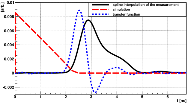
Fig. 1 shows the elements used in the determination of the transfer function : the spline-interpolated measured current transient , the simulated current transient before convolution , and obtained as described. As shown in Fig. 3 the transients for electrons and holes at 1000 V are very similar implying that at high fields around 50 kV/cm the drift velocities of electrons and holes are also similar. As a result, for IR at 1000 V, which is a superposition of electron and hole drift, is to a good approximation a straight line without a tail from slower holes. The time step for all curves is 10 ps. The time shift between the simulated and the measured transient is arbitrary. It does not change the shape of R, but just its position along the time axis.
Comparison of measurements with simulations
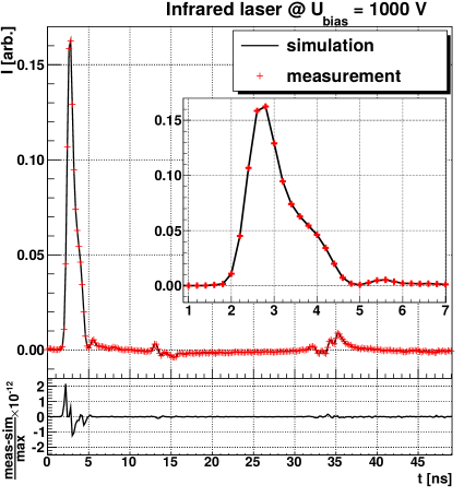
Fig. 2 compares the current transient for the IR measurement at 1000 V with the simulated transient using for the convolution the transfer function determined from the same data. For the simulation only the values at the times at which data were recorded are shown. Both the main pulse, shown as insert, as well as the signal reflections are well described. The difference between the measured and the simulated signal divided by the maximum value of the measured signal is shown at the bottom. Its absolute value is smaller than . This demonstrates the consistency of the method used for determining the electronics transfer function.
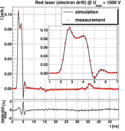
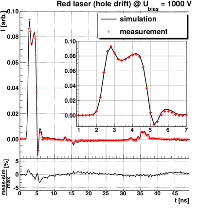
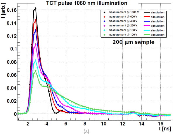
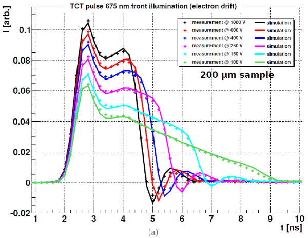
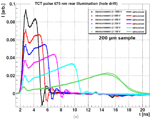
Fig. 3 compares the current transients for the and for the measurement at 1000 V with the simulated transients using for the convolution the transfer function determined from the IR measurement at 1000 V. We note that the transients are very similar and that the pulse is only slightly longer than the pulse. At 1000 V the electric field in the sensors varies between 46 kV/cm and 54 kV/cm. We conclude that for silicon the drift velocities of electrons and holes at these high fields are similar with little dependence on the electric field. The difference between the measured and the simulated signal divided by the maximum value of the measured signal is displayed at the bottom. Its absolute value is less than 5 %. This difference provides an idea of the accuracy of the simulation and the method used for determining the transfer function since the simulated transient before convolution for IR is significantly different compared to the ones for e and h which are to first approximation boxcar functions.
Fig. 4 compares the measured with the simulated current transients for bias voltages between 100 and 1000 V for . It is seen that for all voltages the data are well described by the simulation.
Fig. 5 compares the measured with the simulated current transients for bias voltages between 100 and 1000 V for . With the exception of the 100 V data, the data are well described by the simulations. The biasing voltage of 100 V is only 12.5 V above the depletion voltage, and the effect of the junction where the charges are generated, and of the transition, which the electrons reach at the higher drift times, may be significant.
Fig. 6 compares the measured with the simulated current transients for bias voltages between 100 and 1000 V for . Again, with the exception of the 100 V data, the data are well described by the simulations. At 100 V the electron-hole pairs are generated by the laser light in the low-field region of the sensor. As the density of the generated electron-hole pairs of cm-3 is similar to the doping density, the so called plasma effect [18, 19] is expected to occur at low bias voltages. The plasma effect is due to the shielding of the sensor field by the counter field of the overlapping electron-hole clouds which results in a delayed charge collection. In the simulations the plasma effect is not included. We note that the measured current transients for voltages between 150 and 1000 V are well described by the simulations using the transfer function determined by the method described in the paper from the measurement with 1060 nm laser light at 1000 V.
The transfer functions have also been determined for the silicon pad diodes with different thicknesses and capacitances mentioned on page 1. It is found that, although there are significant differences in the transfer functions, the measurements can be well described with consistent values for the field dependence of the electron and hole mobilities. This demonstrates the validity of the proposed method of determining electronic transfer functions.
Practical aspects of the determination of the transfer function
We conclude the manuscript with a few comments on the experience we made, when we developed the method of determining the transfer function described in this Technical Note. Initially we used a SPICE simulation of detector, cables and readout electronics. Details are given in Ref. [7], where it is also shown that a number of parasitic elements had to be included in the simulation to achieve an acceptable description of the measurements. However, the results never have been fully satisfactory especially for diodes with a capacitance above full depletion below 10 pF. We then used the method described here and obtained satisfactory results from the beginning. To better understand the method and its possible applications, the following studies have been made.
As we do not know, if the current recorded by the oscilloscope is the instantaneous current or the current averaged over the sampling interval, the difference between a simulation using the value at the bin center and the average value has been investigated. Differences were observed at the maxima and minima of the transients, however, they are smaller than % of the maximum signal and do not change significantly the results of the analyses.
For the Fast-Fourier-Transform of the spline-interpolated measurement we included ns of the measurement before the pulse has reached % of the maximum. Additionally, we had to add at least 3 bins ( ps) which are set to zero at the start of . Otherwise, we sometimes experienced oscillations in the transfer function.
We have investigated which of our data should be used for obtaining the optimal transfer function. We find that the best overall description of the complete data set is obtained, if the measurement at 1000 V is used. Our explanation is that the uncertainties of the simulation are smallest for these conditions. At the and sides, there are shallow non-depleted regions as well as high-field regions from the doping gradients, which have not been taken into account in the simulation. For the red laser a significant fraction of the pairs is generated in these regions, whereas for the infrared laser the charges are generated throughout the sensor. In addition, at 1000 V the electric field in the m thick sensor is high; therefore, the variations of the drift velocities, which approach the saturation velocities, are minimal. We conclude: The precise simulation of the transient induced in electrodes of the sensor is one necessary condition for the successful application of the proposed method.
Next we discuss the requirements for noise and sampling frequency. Ideally the sampling step should be small compared to the width of the transfer function. In our example, however, the sampling step of 200 ps is not much shorter than the measured rise time of about 600 ps. As the simulated rise time of the current induced in the electrodes is much shorter, the measured rise time is approximately equal to the width of the main peak of the transfer function. However, if the noise of the transient measurement is small, which has been achieved by injecting pairs per pulse and averaging 512 pulses, an interpolation of the measurements can give reliable results. We have used a 5th order spline interpolation for obtaining data in 10 ps steps from the measured transients which were recorded in 200 ps steps. Thus, the second necessary condition for a successful application of the proposed method are a high signal-to-noise ratio and sampling steps shorter than the rise time of the transient.
Last but not least: the transfer function, which has been determined from a measurement for which the intrinsic detector response could be simulated precisely, can only be used for analyzing data from a sensor with similar parameters, with the capacitance being the most important one.
Acknowledgments
We would like to thank Julian Becker for making available his program which simulates the current transients in silicon pad diodes and for many helpful discussions, Jörn Schwandt for making the TCAD simulations of the electric field which takes into account the and transition regions, and Erika Garutti and Ulrich Koetz, who proof-read the manuscript and made valuable suggestions. We are also grateful to the HGF Alliance Physics at the Terascale which had funded the TCT set-up used for the measurements.
Bibliography
References
- [1] G. Kramberger, V. Cindro, I. Mandic, M. Mikuž, M. Milovanović, M. Zavrtanik, and K. Žagar. Investigation of irradiated silicon detectors by edge-tct. Nuclear Science, IEEE Transactions on, 57(4):2294–2302, Aug 2010.
- [2] M. Mikuž, V. Cindro, G. Kramberger, I. Mandić, and M. Zavrtanik. Study of anomalous charge collection efficiency in heavily irradiated silicon strip detectors. Nuclear Instruments and Methods in Physics Research Section A: Accelerators, Spectrometers, Detectors and Associated Equipment, 636(1, Supplement):S50 – S55, 2011. 7th International Hiroshima Symposium on the Development and Application of Semiconductor Tracking Detectors.
- [3] N. Pacifico, I. D. Kittelmann, M. Fahrer, M. Moll, and O. Militaru. Characterization of proton and neutron irradiated low resistivity p-on-n magnetic czochralski ministrip sensors and diodes. Nuclear Instruments and Methods in Physics Research Section A: Accelerators, Spectrometers, Detectors and Associated Equipment, 658(1):55 – 60, 2011. {RESMDD} 2010.
- [4] M. Swartz, V. Chiochia, Y. Allkofer, D. Bortoletto, L. Cremaldi, S. Cucciarelli, A. Dorokhov, C. H̦rmann, D. Kim, M. Konecki, D. Kotlinski, K. Prokofiev, C. Regenfus, T. Rohe, D.A. Sanders, S. Son, and T. Speer. Observation, modeling, and temperature dependence of doubly peaked electric fields in irradiated silicon pixel sensors. Nuclear Instruments and Methods in Physics Research Section A: Accelerators, Spectrometers, Detectors and Associated Equipment, 565(1):212 Р220, 2006. Proceedings of the International Workshop on Semiconductor Pixel Detectors for Particles and Imaging {PIXEL} 2005 International Workshop on Semiconductor Pixel Detectors for Particles and Imaging.
- [5] C. Scharf. Measurement of the drift velocities of electrons and holes in high-ohmic silicon. MSc thesis, University of Hamburg, Feb. 2014. DESY-THESIS-2014-015.
- [6] J. Becker, E. Fretwurst, and R. Klanner. Measurements of charge carrier mobilities and drift velocity saturation in bulk silicon of and crystal orientation at high electric fields. Solid-State Electronics, 56(1):104 – 110, 2011.
- [7] J. Becker. Signal development in silicon sensors used for radiation detection. PhD thesis, University of Hamburg, 2010. DESY-THESIS-2010-33.
- [8] Hamamatsu Photonics K.K. http://www.hamamatsu.com/.
- [9] Phillips Scientific Fast Pulse Amplifier Model 6954 with some modifications. http://www.phillipsscientific.com/pdf/6954ds.pdf/.
- [10] W. Treberspurg, T. Bergauer, M. Dragicevic, and B. Lutzer. Analysis of test structures and process technology. HEPHY Vienna, 2013. Workshop on Silicon Strip Sensors for the CMS Phase II Upgrade.
- [11] Advanced Laser Diode Systems A.L.S. GmbH. Picosecond Injection Laser; (PiLas) Owner’s Manual. http://alsgmbh.de/.
- [12] S.M. Sze and Kwok K. Ng. Photodetectors and Solar Cells, pages 663–742. John Wiley & Sons, Inc., 2006.
- [13] G. Kramberger. Signal development in irradiated silicon detectors. PhD thesis, University of Ljubljana, 2001.
- [14] SYNOPSIS-TCAD. http://www.synopsys.com/Tools/TCAD/.
- [15] Jörn Schwandt. Private communication.
- [16] C. Scharf and R. Klanner. Measurement of the drift velocities of electrons and holes in high-ohmic silicon. to be submitted to Nuclear Instruments and Methods in Physics Research Section A: Accelerators, Spectrometers, Detectors and Associated Equipment.
- [17] C Jacoboni, C Canali, G Ottaviani, and A Alberigi Quaranta. A review of some charge transport properties of silicon. Solid-State Electronics, 20(2):77–89, 1977.
- [18] R.N. Williams and E.M. Lawson. The plasma effect in silicon semiconductor radiation detectors. Nuclear Instruments and Methods, 120(2):261 – 268, 1974.
- [19] J. Becker, K. Gärtner, R. Klanner, and R. Richter. Simulation and experimental study of plasma effects in planar silicon sensors. Nuclear Instruments and Methods in Physics Research Section A: Accelerators, Spectrometers, Detectors and Associated Equipment, 624(3):716 – 727, 2010.