Tuning Photoinduced Terahertz Conductivity in Monolayer Graphene: Optical Pump Terahertz Probe Spectroscopy
Abstract
Optical pump-terahertz probe differential transmission measurements of as-prepared single layer graphene (AG) (unintentionally hole doped with Fermi energy at 180 meV), nitrogen doping compensated graphene (NDG) with 10 meV and thermally annealed doped graphene (TAG) are examined quantitatively to understand the opposite signs of photo-induced dynamic terahertz conductivity . It is negative for AG and TAG but positive for NDG. We show that the recently proposed mechanism of multiple generations of secondary hot carriers due to Coulomb interaction of photoexcited carriers with the existing carriers together with the intraband scattering can explain the change of photoinduced conductivity sign and its magnitude. We give a quantitative estimate of in terms of controlling parameters - the Fermi energy and momentum relaxation time . Further, the cooling of photoexcited carriers is analyzed using super–collision model which involves defect mediated collision of the hot carriers with the acoustic phonons, thus giving an estimate of the deformation potential.
I Introduction
The performance of electronic and optoelectronic devices depends on the material properties such as carrier mobility, energy conversion efficiency from photon to electron-hole pairs, spectral response and equilibration of the photo-generated carriers. The linear band dispersion with zero band gap in monolayer graphene responsible for many fascinating transport phenomena and optical effects makes graphene a desirable material for high speed optoelectronic devices.Bonaccorso et al. (2010); Novoselov et al. (2005); Morozov et al. (2008); Avouris (2010); Geim and Novoselov (2007); Weis et al. (2012); Bao and Loh (2012) A key question to answer in optoelectronic applications is the relaxation of the hot carriers in conical energy-momentum space of the monolayer graphene. Ultrafast time resolved pump-probe spectroscopy Wang et al. (2010a); Choi et al. (2009); Dawlaty et al. (2008); George et al. (2008); Sun et al. (2010) and angle resolved photoemission spectroscopy Gierz et al. (2013) have been shown to be excellent probes of non-equilibrium carrier dynamics in graphene. The terahertz probe pulse following the optical pump examines the intraband scattering dynamics as compared to optical probe which is sensitive to both interband and intraband scattering processes. Following the pump pulse, the photoexcited carriers achieve a quasi-equilibrium Fermi-Dirac distribution characterized by electron temperature mostly by carrier-carrier scattering. The cooling of the carriers can occur through phonon emission as well as through carrier-carrier scattering. The latter involves the transfer of energy of photoexcited carriers to the existing carriers in graphene (making them hot). Song et al. (2013, 2011); Tielrooij et al. The cooling via phonon emission involving optical phonons occurs on a time scale of 100 to 500 fs till the energy of the photoexcited carriers is less than the optical phonon energy (200 meV). This is followed by the direct coupling between the carriers and acoustic phonons which can last for tens of ps. However the carrier-acoustic phonon relaxation time is reduced to less than 10 ps when large momentum and large energy acoustic phonons emission occurs mediated by the disorder. This three body (carriers + acoustic phonons + disorder) mediated cooling is termed as super collision cooling of the carriers. Graham et al. (2013) Several groups have reported optical pump - terahertz probe (OPTP) time domain spectroscopy of epitaxial grown as well as CVD grown graphene showing positive Choi et al. (2009); Sun et al. (2010); Strait et al. (2011) as well as negative dynamic conductivity. Tielrooij et al. ; Docherty et al. (2012); Jnawali et al. (2013); Frenzel et al. (2013) The positive dynamic conductivity can be easily understood in terms of intraband scattering of the carriers. Docherty et al. Docherty et al. (2012) showed that the THz photoconductivity changes from positive in vacuum to negative in nitrogen, air and oxygen environment and proposed stimulated THz emission from photoexcited graphene as the cause of the negative photoconductivity. Several other experimental Karasawa et al. (2011) and theoretical Ryzhii et al. (2007); Satou et al. (2013) studies have also attributed the negative dynamic conductivity to the amplified stimulated terahertz emission above a threshold pump intensity. Otsuji et al. (2012) In this context, Gierz et al. Gierz et al. (2013) have shown experimentally that only within 130 fs after photoexcitation, the Fermi-Dirac distribution for electron and holes are different, suggesting that population inversion and hence stimulated emission is not feasible beyond this time window. Jnawali et al. Jnawali et al. (2013) have attributed the decrease in photoconductivity to the increase in carrier scattering rate with negligible increase of Drude weight. Tielrooij et al.Tielrooij et al. have proposed to explain the negative dynamic conductivity via Coulomb interaction governed carrier-carrier scattering where the energy of the photo-excited carriers is transferred to the existing carriers in the Dirac cone, a process termed as secondary hot carrier generation (SHCG). While preparing our manuscript we came across a recent study of tuning the sign of OPTP signal from the SLG using electrostatic top gating. Shi et al. (2014) Their explanation is as follows: Taking conductivity , the dynamic conductivity where is the Drude weight and is carrier scattering rate and the subscript 0 stands pump off condition. The contribution from Drude weight dominates near charge neutral point and is positive. For higher doping, the contribution from change of scattering rate controls the . The authors assumed Shi et al. (2014) , independent of to explain the negative dynamic conductivity. This framework does not explain the observed saturation behavior of the dynamic conductivity at higher Fermi energy. Therefore, the issue of the optical pump induced terahertz conductivity, in particular its sign and amplitude is still open and needs to be understood quantitatively.
In this work, we report the THz conductivity of (1) as-grown single layer graphene (AG) by chemical vapor deposition which is unintentionally hole doped, (2) nitrogen doped monolayer graphene (NDG) and (3) thermally annealed nitrogen doped graphene (TAG). The samples have different values of carrier momentum relaxation time and the Fermi energy . The conductivities obtained from the THz transmission measurements compare well with the estimates from the relative Raman intensities of D and G bands. Next, we present optical pump (1.58 eV) - THz probe measurements of the transient THz photoconductive response of the graphene samples. On photo-excitation, the dynamic conductivity ( is negative for the AG but positive for the NDG. In both cases, the ||is 1.5 where is quantum of conductance. We show that on thermal annealing of the NDG, the is once again negative. A quantitative analysis of is done by noting that in the terahertz range, intraband scattering contribution to is orders of magnitude larger than the interband contribution. We invoke secondary hot carrier generation (SHCG) Tielrooij et al. to explain quantitatively the negative in AG. The sign and magnitude of the dynamic conductivity in graphene thus depends on the relative contributions of the intraband scattering and the SHCG, which, in turn, depend on the momentum relaxation time and the Fermi energy. The cooling of hot carriers is quantitatively analyzed in terms of super-collision (SC) processes. The frequency dependence of dynamic conductivity is also measured.
II method
II.1 Terahertz Set Up
The output beam of the Ti: sapphire regenerative amplifier laser system which produces 50 fs optical pulses at a central wavelength of 785 nm with a repetition rate of 1 KHz is divided into three parts: for terahertz generation, terahertz detection and optical pumping. The terahertz radiation is generated by co-focusing the fundamental and its second harmonic beam using 10 cm focal length lens to produce plasma in air. The unwanted light following the plasma was blocked using high resistive silicon wafer. The terahertz was collimated and focused on the sample by a pair of off-axis parabolic mirrors and again collimated and focused by parabolic mirrors on a 1 mm thick ZnTe crystal used as detector. All experiments were carried out in nitrogen environment at room temperature. The estimated terahertz electric field is 30 kV/cm. The optical pump-induced changes in the terahertz transmission were measured at the maximum position of the terahertz electric field. The spot size of the pump beam was 0.7 cm and the spot size of the terahertz beam was 0.3 cm so that the pump can excite the sample uniformly. To measure the photoinduced transmission the chopper (341 Hz) was placed in the pump path and to measure the THz electric field from the unexcited sample, the chopper was placed in the path of the terahertz beam. All experiments were performed in transmission geometry.
II.2 Sample Preparation
The graphene samples were grown by using the well-known chemical vapor deposition (CVD) method on 25 thick copper foil.Li et al. (2009) Before growth, the copper foils were cleaned through a chemical process using acetone, acetic acid, deionised water, isopropyl alcohol and methanol successively. In order to remove the oxides and chemical residues, the copper substrates were heated at 1000oC for 30 minutes in presence of hydrogen at a pressure of 20 Torr. Subsequently, methane was flown into the chamber, and graphene growth was carried out for 30 minute keeping hydrogen and methane at a fixed ratio of 1:3, followed by stoppage of the methane flow and the system allowed to cool at a rate of 20oC/min for first 20 minutes without changing the hydrogen flow rate. Then, the system was cooled by a normal fan up to a temperature of 350oC in 1 hr., followed by natural cooling to room temperature. For nitrogen doping, protocol was similar to that reported recently.Lv et al. (2012) Namely, after stopping the methane flow and cooling the system to 850oC, ammonia (10 sccm) was passed for 10 min. Subsequently, ammonia flow was stopped and the system was cooled in hydrogen atmosphere as described before. Graphene was transferred onto the 1 mm thick -quartz by the PMMA technique.Suk et al. (2011)
III results and discussions
III.1 Characterization of the Sample
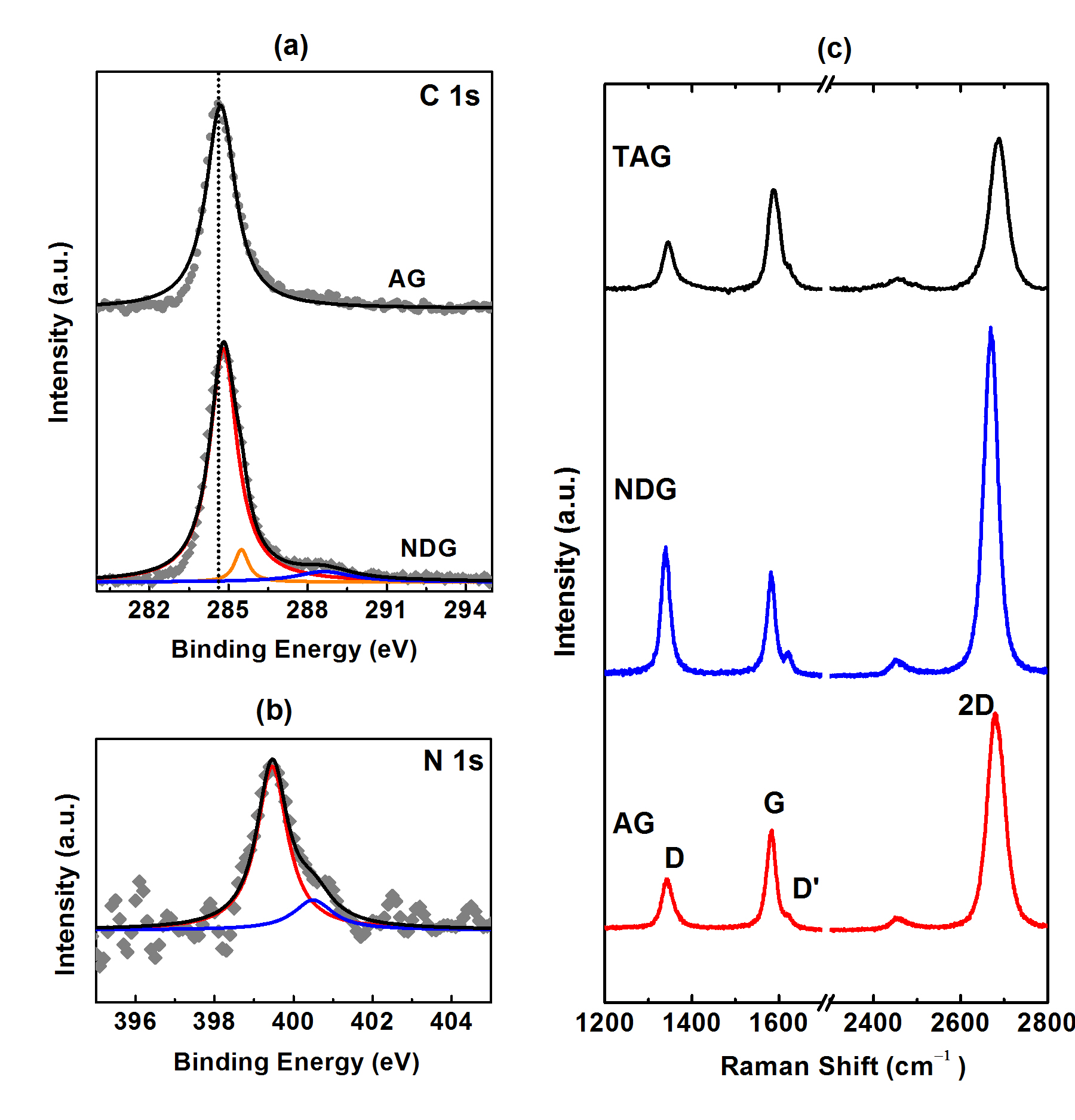
Primarily, the experiments were carried out on two samples: AG and NDG. Later, to check the effect of temperature annealing the NDG was annealed at C for 4 hrs in argon atmosphere and all the experiments were also performed on this thermally annealed graphene (TAG). The x-ray photoemission spectroscopy (XPS) was done to confirm the presence and nature of nitrogen in graphene. The samples were further characterized by Raman spectroscopy at room temperature using = 514 nm of laser light.
The C 1s XPS spectra for AG and NDG are shown in Fig.1a. The peak occurs at binding energy of 284.6 eV for AG corresponding to carbon. Wang et al. (2010b) For NDG the peaks are at 284.8 eV, 285.8 eV and 288.5 eV corresponding to carbon, CN and C=O bonds. Wang et al. (2010b) The N 1s XPS spectra of NDG sample shown in Fig.1b is fitted with two peaks corresponding to non-graphitic substitution namely, pyridinic (399.5 eV) and pyrrolic (400.5 eV) N. Wang et al. (2010b); Gao et al. (2012) In the pyridinic and pyrrolic structures N-atom bonds with two carbon atoms. We cannot resolve any quaternary (graphitic) substitution of N (generally occurs at a binding energy of 401 eV).
| Sample | G() | D() | I(2D)/I(G) | A(D)/A(G) | I(D)/I(D′) | (meV) | (nm) | (fs) |
|---|---|---|---|---|---|---|---|---|
| AG | 1583 | 1343 | 2.4 | 0.6 | 7.0 | 180 | 34 | 34 |
| NDG | 1582 | 1340 | 3.5 | 1.3 | 8.7 | 10 | 15 | 15 |
| TAG | 1589 | 1346 | 1.5 | 0.5 | 5.7 | 200 | 38 | 38 |
Raman spectra of the samples are recorded at room temperature using the excitation wavelength = 514 nm, displaying four bands (Fig.1c) where peak positions and relative intensities are given in Table 1. The G band is symmetry allowed zone-center point longitudinal and transverse optical phonon and the D band is associated with the disorder activated near zone-boundary (K point) transverse optical phonon.Malard et al. (2009) The 2D band is due to second-order Raman scattering from near K-point transverse optical phonons and is an unambiguous finger print of the number of layers, as understood by double resonance Raman scattering. Malard et al. (2009) The D′ band is associated with the disorder activated near -point longitudinal optical phonons.The frequencies of the 2D and G bands and their relative intensities depend on the doping levels. Das et al. (2008) It is known that CVD grown graphene can be unintentionally p-doped due to unwanted charge transfer doping from H2O/O2 molecules. Shin et al. (2012) Using the intensity ratio of the 2D and G bands I(2D)/I(G), the Fermi energy of the AG graphene is 180 meV.Das et al. (2008) After N-doping the intensity ratio I(2D)/I(G) increases which suggests Das et al. (2008) that the N-doping has compensated the p-doping in the AG shifting the Fermi level close to Dirac point with 10 meV. However the exact value of is difficult to estimate from the Raman data of NDG. The increase in the intensity of the D and D′ bands after nitrogen doping clearly reveals an increase in the disorder in NDG. The ratio of the D and G band integrated intensities A(D)/A(G) increase from 0.6 in AG to 1.3 in NDG. The ratio A(D)/A(G) is empirically related to the in-plane crystalline grain size without defects () as : Cançado et al. (2006) A(D)/A(G) = which gives La 34 nm for the AG, 15 nm for the NDG and 38 nm for the TAG. Assuming the transport mean free path of the carriers and using Fermi velocity m/s, Castro Neto et al. (2009) the average momentum relaxation time is 15 fs in NDG, 34 fs in AG and 38 fs in TAG. One may try to estimate estimate the conductivity of the graphene in the strong scattering limit Tielrooij et al. by using , giving for AG, for NDG and for TAG. The intensity ratio of D and D′ bands, I(D)/I(D′), has been related to the type of defects. Eckmann et al. (2012) For the AG I(D)/I(D′) 7 implies vacancy-like defects; I(D)/I(D′) 8.7 in NDG implies a presence of sp3 defects ( for defects, I(D)/I(D13). Eckmann et al. (2012)
III.2 Terahertz conductivity of graphene
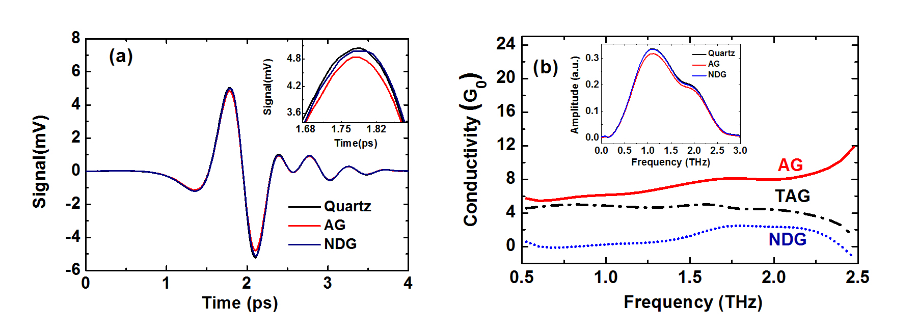
Let the temporal evolution of the transmitted terahertz electric fields through the graphene on the -quartz substrate and through the substrate without graphene be denoted by Tsam(t) and Tref(t), respectively. The ratio of Fourier transform (FT) of Tsam(t) and Tref(t) gives amplitude and phase of the spectral transmission function: S()=Tsam(t)/ Tref(t). The complex conductivity spectra can be obtained from the spectral transmission function by using the relation in the limit of thin film approximation. Tomaino et al. (2011); Tinkham (1956) Here Z0 = 377 is the impedance of free space and is refractive index of substrate taken as 2.2. Figure 2a shows the temporal terahertz fields through quartz (black line), AG (red line) and NDG (blue line). Figure 2b shows the real part of the conductivity in the spectral range 0.5 THz to 2.5 THz and the corresponding FTs are shown in the inset. A nearly spectrally flat conductivity suggests large momentum scattering rate for the graphene samples i.e. , George et al. (2008); Strait et al. (2011); Liu et al. (2011) as also suggested by the estimates of from the Raman data (see Table.1). The average conductivities of AG, NDG and TAG samples are (7 1)G0, (1.5 0.5)G0 and (4 1)G0 respectively, in close agreement with the estimates obtained from the Raman data. As mentioned earlier, the reduction of conductivity of the NDG is due to the shift of the Fermi level towards the Dirac point and a decrease of the momentum relaxation time due to increase in disorder.
III.3 Optical Pump Induced Changes in Terahertz Conductivities
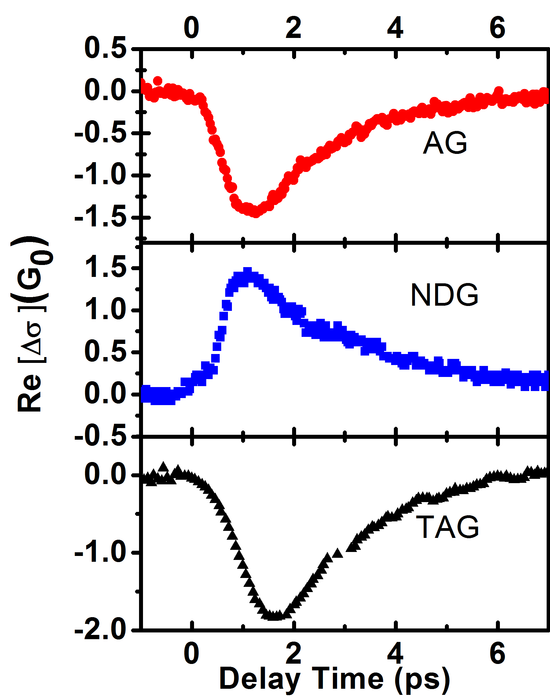
The differential transmission, T/T is related to the dynamic THz conductivity, by the relation . The results shown in Fig.3 correspond to the peak of THz electric field using pump excitation density of 340 J/cm2 per pulse. Taking the absorption at 785 nm to be 2.3, photo-excited carrier density is 3 1013 /cm2. Mak et al. (2008) Most interestingly, is negative for the AG whereas it is positive for the NDG. After annealing the NDG, is once again negative for TAG.
We now analyze various contributions to the dynamic conductivity. As mentioned earlier, hot carriers achieve quasi equilibrium Fermi distribution with electron temperature Te, thus , where T0 is the lattice temperature ( = 300 K). The intraband and interband contributions to dynamic conductivity is calculated using. Winnerl et al. (2011)
| (1) |
| (2) |
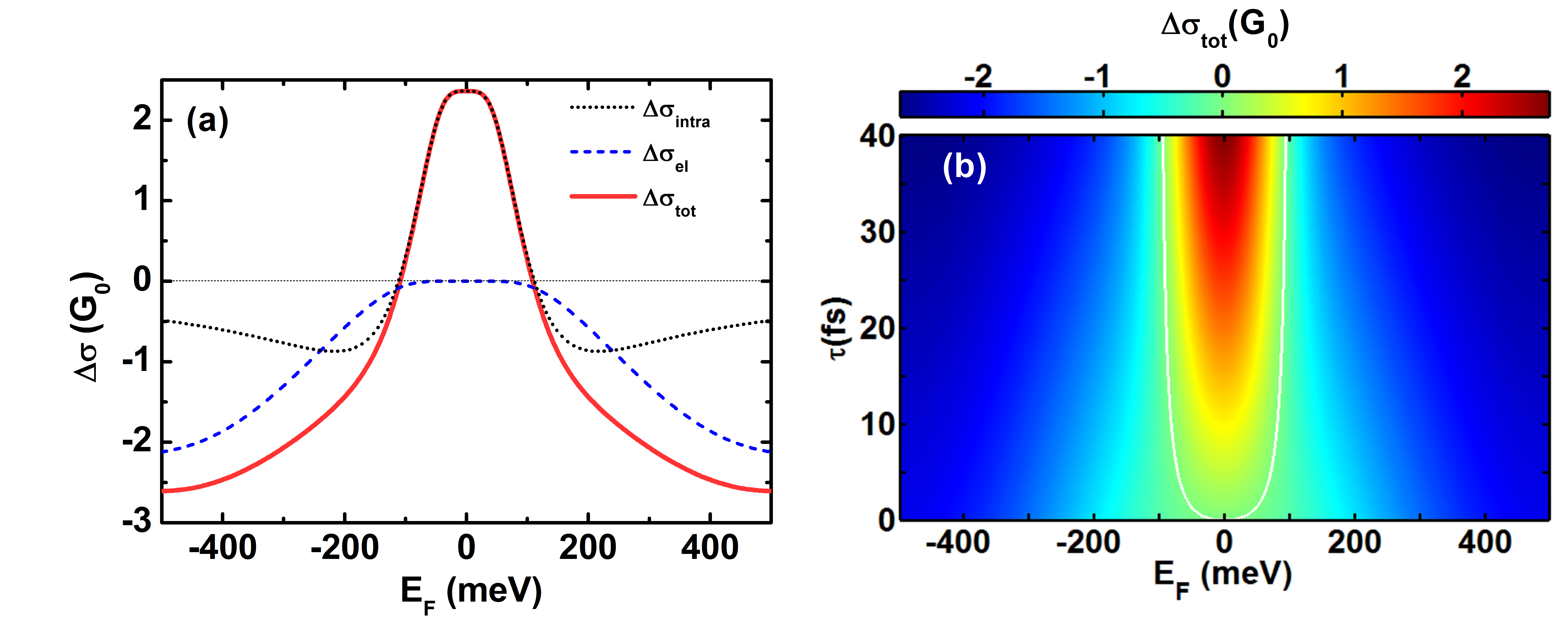
where is terahertz probe frequency. The interband contribution sup gives positive and negative depending on but is times smaller as compared to the intraband contribution. Hence the photoinduced terahertz conductivity is dominated by the intraband scattering George et al. (2008); Strait et al. (2011); Winnerl et al. (2011) and therefore we will neglect interband contributions. Taking = 34 fs, the intraband contribution to the dynamic conductivity at 1 THz is shown in Fig.4a (dotted black line) as a function of Fermi energy at a representative Te = 700 K. The magnitude of as seen in Fig.4a is not sufficient to explain the observed in AG (E180 meV) which necessarily requires another mechanism. We consider the recently proposed secondary hot carrier generation (SHCG) Tielrooij et al. in which the photoexcited carriers interact with the intrinsic carriers to excite the later. The photoexcited carriers have two scattering channels; one is the conventional intraband scattering mechanism with momentum relaxation time, as discussed earlier and the other is the Coulomb scattering with momentum relaxation time, which is proportional to carrier energy i.e., where b, the proportionality constant, depends on the ratio of the average inter-electron Coulomb interaction energy to the Fermi energy and the density of the secondary hot carriers (ni) (see Eq. 3.21 of Ref.Das Sarma et al., 2011). The secondary hot carrier generation contribution to the photoinduced conductivity is given by Tielrooij et al.
| (3) |
| (4) |
where is density of states of graphene at Fermi energy. As suggested in Ref .Tielrooij et al., we take = 34 fs and EF = 180 meV to get b = 190 fs/eV in calculating . Figure 4a (dashed blue line) shows that and the magnitude is comparable to the intraband contribution to the terahertz dynamic conductivity. The total change of terahertz photoconductivity is the sum of intraband and the SHCG contributions: . Figure 4b shows the dynamics terahertz photoconductivity at 1 THz as a function of Fermi energy and momentum relaxation time at a representative electron temperature of 700 K. It shows that the magnitude and sign of is determined by the value of the Fermi energy and the momentum relaxation time. In AG, 180 meV and 34 fs, resulting in negative . In contrast, a shift of Fermi level towards the Dirac point in NDG results in due to dominance of the intraband scattering process. Again, in TAG the increased Fermi energy lead to . The results are similar for other representative values of parameter b (b = 120, 300 fs/ev) sup
III.4 Cooling Dynamics
We now focus on the cooling dynamics of the hot carriers. It is known Gierz et al. (2013); Lui et al. (2010); Kampfrath et al. (2005) that photoexcited electrons can efficiently lose their energy by emitting optical phonons with energy 200 meV with a relaxation time of 300 to 500 fs. Below 200 meV, the hot carriers can dissipate energy only by emitting acoustic phonons with energy per scattering event as permitted by conservation of momentum. Here, is Bloch-Grüneisen temperature given by ( is velocity of sound in graphene) which defines a boundary between the low and the high temperature behavior. The cooling of carriers can last as long as 300 ps for phonon temperatures . However, according to the super collision (SC) modelSong et al. (2012) an alternate route of energy relaxation of the hot carriers is via the disorder-mediated emission of high energy () and high momentum () acoustic phonons. The enhancement factor for energy dissipation rate over momentum conserving path ways is expressed as Song et al. (2012)
| (5) |
Therefore, the enhancement factor depends on temperature, Fermi energy and disorder. The temperature is 87 K for AG and 5 K for NDG which are less than (= 300 K). According to Eq. 5 the enhancement factor is 17380 for NDG and 13 for AG, taking = 700 K and = 300 K showing the dominance of the SC cooling.
For the SC mechanism the heat dissipation rate is given bySong et al. (2012) where where g is electron-phonon coupling strength and is the deformation potential. After acheiving the quasi-equilibrium temperature , subsequent decreases of the carrier temperature due to the SC is described by Song et al. (2012)
| (6) |
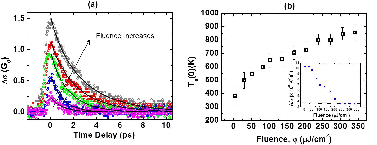
where is the SC rate coefficient. To fit the data shown in Fig.5a, one should in principle use a sum of two terms: first term is an exponential term with relaxation time hundreds of femtosecond to represent the contribution of the optical phonons and a second term given by the solution of Eq.6 for the SC mechanism. However we find that our data is not very sensitive to the contributions from the term representing the optical phonons and hence Figure 5a shows the fitting of transient conductivity of the NDG with the SC model described by Eq.6 with and as fitting parameters. Here, we have used Eq.1 and Eq.3 to calculate dynamic conductivity, taking = 15 fs and = 10 meV as suggested by our Raman data. Figure 5b shows fluence dependence of the fitting parameter and the inset shows saturation of at high fluence suggesting that the SC dominates over momentum conserving paths at higher fluences.
The SC cooling rate coefficient is :Song et al. (2012)
| (7) |
where
| (8) |
where is Reimann zeta function and kg/m2 is density of graphene. Therefore, the SC rate coefficient depends on the graphene sample and will not vary with the number of photoexcited carriers at higher fluence where the SC cooling dominates. The SC cooling dominated can be used to estimate the deformation potential of graphene. Taking = 10 meV, and , the deformation potential is 28 eV, comparable to the reported values of 10 - 30 eV. Bolotin et al. (2008); Dean et al. (2010)
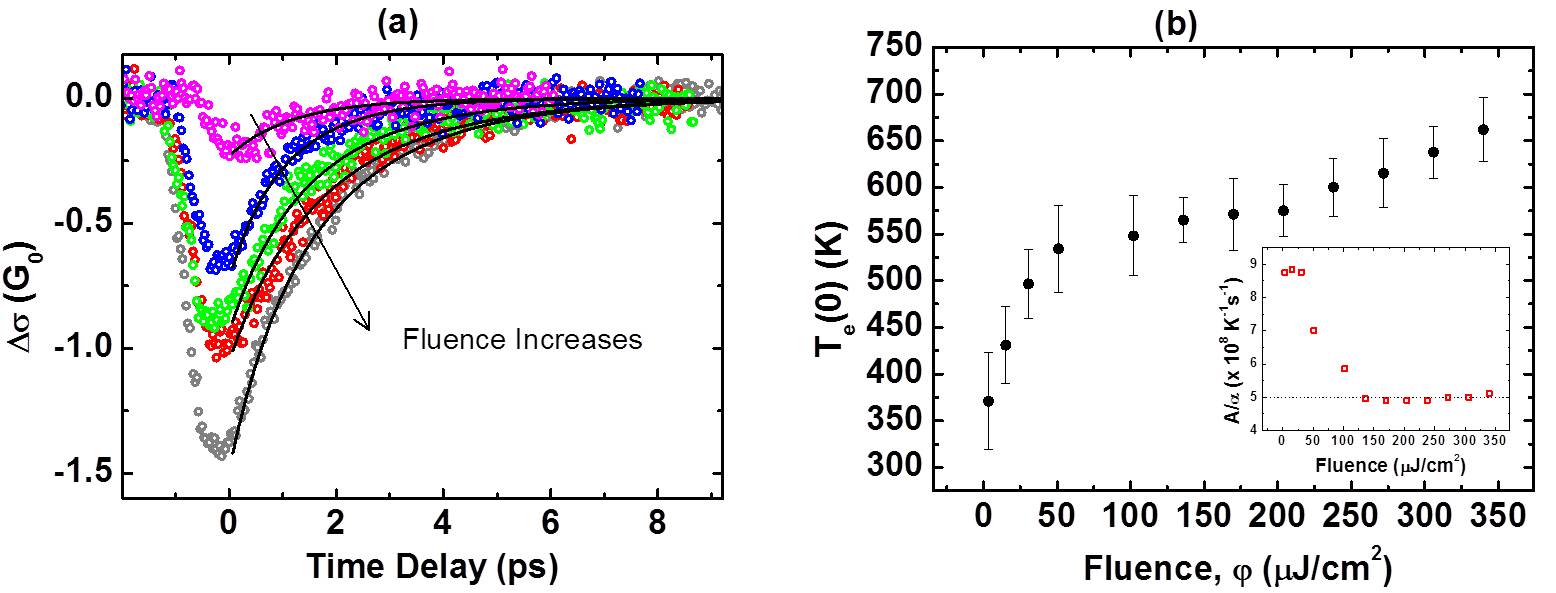
In a similar manner, the relaxation dynamics of AG is fitted with SC model using Eq. 1, 3 and 6. The fitted graphs shown in Fig.6a are generated using = 34 fs, b = 190 fs/eV and (at 300 K) = 180 meV. The fluence dependence of the fitted parameters and are shown in Fig.6b. At higher fluences saturates at (shown in the inset), which gives (using 6) the deformation potential 17 eV. Since, the electron heat capacity of graphene is proportional to density of state and hence the Fermi energy, Shi et al. (2014); Song et al. (2012) the NDG will have smaller electronic heat capacity than that of AG and therefore the electron temperature in NDG will be more than that in AG for a given pump fluence. This is indeed the case since K in AG and K in NDG at .
III.5 Frequency dependence of dynamic conductivity
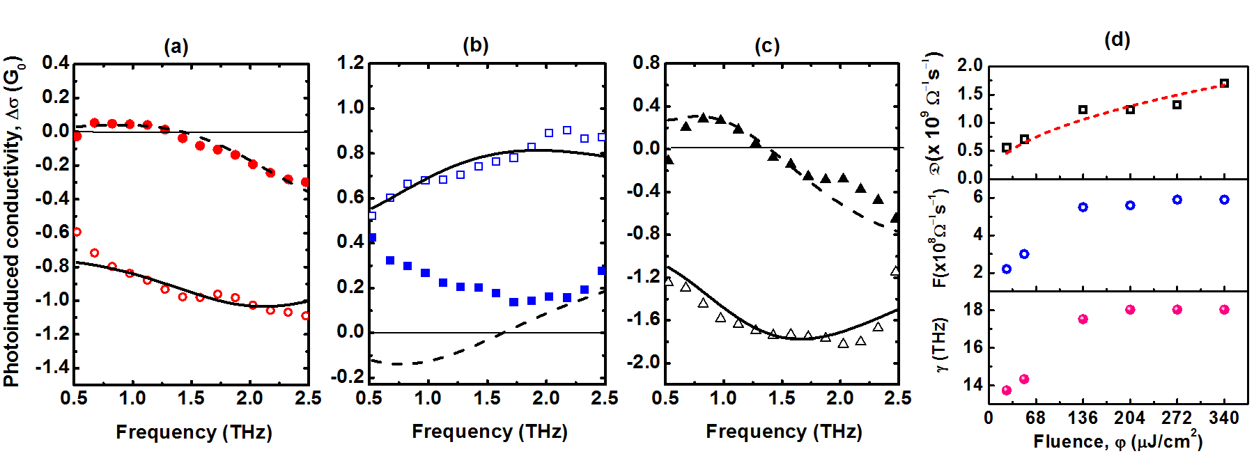
We now present the frequency dependence of the dynamic conductivity. After the pump excitation, the photoinduced change in terahertz electric field, T(t) throughout the complete terahertz pulse is measured sup for a pump fluence of and Figure 7a, 7b and 7c show the corresponding real and imaginary part of photoinduced conductivity for AG, NDG and TAG respectively. In AG the zero crossing of the imaginary part of at 1.3 THz strongly suggests a corresponding peak in the real part of which can be described by a Lorentzian oscillator. However, the amplitude of the imaginary part is much less than the real part and points to the Drude behavior. Hence Drude-Lorentz model has been used to describe the frequency dependence of Docherty et al. (2012); Parkinson et al. (2007, 2009)
| (9) |
Here, the first term is the Drude part in terms of Drude weight and momentum relaxation time . The second term is the Lorentz part with F as the oscillator strength, as linewidth and the resonant frequency. The fitted curves are shown in Fig. 7a for the AG ( = , = 34 fs, F = , = 18 THz, = 2.3 THz). In comparison, for the NDG the imaginary part is positive as in Drude-like response but the positive real part shown in Fig. 7b cannot be explained by the Drude model. The Drude–Lorentz model (Eq. 9) is not able to fit the (Fig. 7b). A poor fit to the imaginary part of needs to be understood. Here, we have used = 15 fs (obtained from Raman scattering) and = 2.0 THz. The of TAG is nearly same as that of the AG and fitted with Drude Lorentz model with = 38 fs and = 1.7 THz, as shown in Fig. 7c.
The dynamic conductivity of the AG is plotted at various the pump fluence varying from 25 to . sup The fittings are performed by taking = 34 fs and = 2.3 THz and varying , F and . The fluence dependence of the parameters , F and are shown in Fig. 7d. It is seen that (see the dotted line in top panel) as expected for graphene ( ). The parameters F and saturate at fluence above . The physical significance of the resonant frequency in Lorentz part of is not clear. Docherty et al.Docherty et al. (2012) have attributed this to the opening of a gap in the density of state.
IV conclusion
In summary, we have presented a quantitative framework of THz dynamic conductivity in monolayer graphene. We showed that is determined by the relative contributions of the secondary hot carrier generation and conventional intraband scattering which, in turn, depend on the position of the Fermi level and momentum relaxation time. In highly doped sample, the photoexcited hot electrons interact with the intrinsic carriers to generate secondary hot carriers which result in decrease of the THz conductivity. In NDG, the Fermi energy is closer to the Dirac point and the enhanced disorder decreases the momentum relaxation time which makes the intraband scattering as the dominant scattering mechanism resulting in positive . The cooling dynamics of the hot carriers is well explained in both the sample by the disorder mediated electron-acoustic phonon interaction, giving the deformation potential comparable to the previous studies.
Acknowledgements.
AKS thanks Nano Mission Project under Department of Science and Technology, India for funding. We thank Gyan Prakash for his help in the initial part of the experiments.References
- Bonaccorso et al. (2010) F. Bonaccorso, Z. Sun, T. Hasan, and A. C. Ferrari, Nat. Photon. 4, 611 (2010).
- Novoselov et al. (2005) K. S. Novoselov, A. K. Geim, S. V. Morozov, D. Jiang, M. I. Katsnelson, I. V. Grigorieva, S. V. Dubonos, and A. A. Firsov, Nature 438, 197 (2005).
- Morozov et al. (2008) S. V. Morozov, K. S. Novoselov, M. I. Katsnelson, F. Schedin, D. C. Elias, J. A. Jaszczak, and A. K. Geim, Phys. Rev. Lett. 100, 016602 (2008).
- Avouris (2010) P. Avouris, Nano Letters 10, 4285 (2010).
- Geim and Novoselov (2007) A. K. Geim and K. S. Novoselov, Nat. Mater. 6, 183 (2007).
- Weis et al. (2012) P. Weis, J. L. Garcia-Pomar, M. Hh, B. Reinhard, A. Brodyanski, and M. Rahm, ACS Nano 6, 9118 (2012).
- Bao and Loh (2012) Q. Bao and K. P. Loh, ACS Nano 6, 3677 (2012).
- Wang et al. (2010a) H. Wang, J. H. Strait, P. A. George, S. Shivaraman, V. B. Shields, M. Chandrashekhar, J. Hwang, F. Rana, M. G. Spencer, C. S. Ruiz-Vargas, and J. Park, Applied Physics Letters 96, 081917 (2010a).
- Choi et al. (2009) H. Choi, F. Borondics, D. A. Siegel, S. Y. Zhou, M. C. Martin, A. Lanzara, and R. A. Kaindl, Applied Physics Letters 94, 172102 (2009).
- Dawlaty et al. (2008) J. M. Dawlaty, S. Shivaraman, M. Chandrashekhar, F. Rana, and M. G. Spencer, Applied Physics Letters 92, 042116 (2008).
- George et al. (2008) P. A. George, J. Strait, J. Dawlaty, S. Shivaraman, M. Chandrashekhar, F. Rana, and M. G. Spencer, Nano Letters 8, 4248 (2008).
- Sun et al. (2010) D. Sun, C. Divin, C. Berger, W. A. de Heer, P. N. First, and T. B. Norris, Phys. Rev. Lett. 104, 136802 (2010).
- Gierz et al. (2013) I. Gierz, J. C. Petersen, M. Mitrano, C. Cacho, I. C. E. Turcu, E. Springate, A. Sthr, A. Khler, U. Starke, and A. Cavalleri, Nat. Mater. 12, 1119 (2013).
- Song et al. (2013) J. C. W. Song, K. J. Tielrooij, F. H. L. Koppens, and L. S. Levitov, Phys. Rev. B 87, 155429 (2013).
- Song et al. (2011) J. C. W. Song, M. S. Rudner, C. M. Marcus, and L. S. Levitov, Nano Letters 11, 4688 (2011).
- (16) K. J. Tielrooij, J. C. W. Song, S. A. Jensen, A. Centeno, A. Pesquera, A. Zurutuza Elorza, M. Bonn, L. S. Levitov, and F. H. L. Koppens, Nat. Phys. 9, 248.
- Graham et al. (2013) M. W. Graham, S.-F. Shi, D. C. Ralph, J. Park, and P. L. McEuen, Nat. Phys. 9, 103 (2013).
- Strait et al. (2011) J. H. Strait, H. Wang, S. Shivaraman, V. Shields, M. Spencer, and F. Rana, Nano Letters 11, 4902 (2011).
- Docherty et al. (2012) C. J. Docherty, C.-T. Lin, H. J. Joyce, R. J. Nicholas, L. M. Herz, L.-J. Li, and M. B. Johnston, Nat. Commun. 3, 1228 (2012).
- Jnawali et al. (2013) G. Jnawali, Y. Rao, H. Yan, and T. F. Heinz, Nano Letters 13, 524 (2013).
- Frenzel et al. (2013) A. J. Frenzel, C. H. Lui, W. Fang, N. L. Nair, P. K. Herring, P. Jarillo-Herrero, J. Kong, and N. Gedik, Applied Physics Letters 102, 113111 (2013).
- Karasawa et al. (2011) H. Karasawa, T. Komori, T. Watanabe, A. Satou, H. Fukidome, M. Suemitsu, V. Ryzhii, and T. Otsuji, Journal of Infrared, Millimeter, and Terahertz Waves 32, 655 (2011).
- Ryzhii et al. (2007) V. Ryzhii, M. Ryzhii, and T. Otsuji, Journal of Applied Physics 101, 083114 (2007).
- Satou et al. (2013) A. Satou, V. Ryzhii, Y. Kurita, and T. Otsuji, Journal of Applied Physics 113, 143108 (2013).
- Otsuji et al. (2012) T. Otsuji, S. Boubanga-Tombet, A. Satou, M. Suemitsu, and V. Ryzhii, Journal of Infrared, Millimeter, and Terahertz Waves 33, 825 (2012).
- Shi et al. (2014) S.-F. Shi, T.-T. Tang, B. Zeng, L. Ju, Q. Zhou, A. Zettl, and F. Wang, Nano Letters 14, 1578 (2014).
- Li et al. (2009) X. Li, W. Cai, J. An, S. Kim, J. Nah, D. Yang, R. Piner, A. Velamakanni, I. Jung, E. Tutuc, S. K. Banerjee, L. Colombo, and R. S. Ruoff, Science 324, 1312 (2009).
- Lv et al. (2012) R. Lv, Q. Li, A. R. Botello-Méndez, T. Hayashi, B. Wang, A. Berkdemir, Q. Hao, A. L. Elías, R. Cruz-Silva, H. R. Gutiérrez, Y. A. Kim, H. Muramatsu, J. Zhu, M. Endo, H. Terrones, J.-C. Charlier, M. Pan, and M. Terrones, Scientific Reports 2, 586 (2012).
- Suk et al. (2011) J. W. Suk, A. Kitt, C. W. Magnuson, Y. Hao, S. Ahmed, J. An, A. K. Swan, B. B. Goldberg, and R. S. Ruoff, ACS Nano 5, 6916 (2011).
- Wang et al. (2010b) Y. Wang, Y. Shao, D. W. Matson, J. Li, and Y. Lin, ACS Nano 4, 1790 (2010b).
- Gao et al. (2012) H. Gao, L. Song, W. Guo, L. Huang, D. Yang, F. Wang, Y. Zuo, X. Fan, Z. Liu, W. Gao, R. Vajtai, K. Hackenberg, and P. M. Ajayan, Carbon 50, 4476 (2012).
- Malard et al. (2009) L. Malard, M. Pimenta, G. Dresselhaus, and M. Dresselhaus, Physics Reports 473, 51 (2009).
- Das et al. (2008) A. Das, S. Pisana, B. Chakraborty, S. Piscanec, S. K. Saha, U. V. Waghmare, K. S. Novoselov, H. R. Krishnamurthy, A. K. Geim, A. C. Ferrari, and A. K. Sood, Nat. Nano. 3, 210 (2008).
- Shin et al. (2012) D.-W. Shin, H. M. Lee, S. M. Yu, K.-S. Lim, J. H. Jung, M.-K. Kim, S.-W. Kim, J.-H. Han, R. S. Ruoff, and J.-B. Yoo, ACS Nano 6, 7781 (2012).
- Cançado et al. (2006) L. G. Cançado, K. Takai, T. Enoki, M. Endo, Y. A. Kim, H. Mizusaki, A. Jorio, L. N. Coelho, R. Magalhães-Paniago, and M. A. Pimenta, Applied Physics Letters 88, 163106 (2006).
- Castro Neto et al. (2009) A. H. Castro Neto, F. Guinea, N. M. R. Peres, K. S. Novoselov, and A. K. Geim, Rev. Mod. Phys. 81, 109 (2009).
- Eckmann et al. (2012) A. Eckmann, A. Felten, A. Mishchenko, L. Britnell, R. Krupke, K. S. Novoselov, and C. Casiraghi, Nano Letters 12, 3925 (2012).
- Tomaino et al. (2011) J. L. Tomaino, A. D. Jameson, J. W. Kevek, M. J. Paul, A. M. van der Zande, R. A. Barton, P. L. McEuen, E. D. Minot, and Y.-S. Lee, Opt. Express 19, 141 (2011).
- Tinkham (1956) M. Tinkham, Phys. Rev. 104, 845 (1956).
- Liu et al. (2011) W. Liu, R. Valdés Aguilar, Y. Hao, R. S. Ruoff, and N. P. Armitage, Journal of Applied Physics 110, 083510 (2011).
- Mak et al. (2008) K. F. Mak, M. Y. Sfeir, Y. Wu, C. H. Lui, J. A. Misewich, and T. F. Heinz, Phys. Rev. Lett. 101, 196405 (2008).
- Winnerl et al. (2011) S. Winnerl, M. Orlita, P. Plochocka, P. Kossacki, M. Potemski, T. Winzer, E. Malic, A. Knorr, M. Sprinkle, C. Berger, W. A. de Heer, H. Schneider, and M. Helm, Phys. Rev. Lett. 107, 237401 (2011).
- (43) See Supplemental Material at [URL will be inserted by publisher] for interband conductivity shown in Fig. s1, contour plot of shown in Fig. s2, the temporal evolution of photoinduced THz pulse shown in Fig. s3 and spectral dependence of photoinduced complex conductivity of AG at different pump fluences shown in Fig. s4.
- Das Sarma et al. (2011) S. Das Sarma, S. Adam, E. H. Hwang, and E. Rossi, Rev. Mod. Phys. 83, 407 (2011).
- Lui et al. (2010) C. H. Lui, K. F. Mak, J. Shan, and T. F. Heinz, Phys. Rev. Lett. 105, 127404 (2010).
- Kampfrath et al. (2005) T. Kampfrath, L. Perfetti, F. Schapper, C. Frischkorn, and M. Wolf, Phys. Rev. Lett. 95, 187403 (2005).
- Song et al. (2012) J. C. W. Song, M. Y. Reizer, and L. S. Levitov, Phys. Rev. Lett. 109, 106602 (2012).
- Bolotin et al. (2008) K. I. Bolotin, K. J. Sikes, J. Hone, H. L. Stormer, and P. Kim, Phys. Rev. Lett. 101, 096802 (2008).
- Dean et al. (2010) C. R. Dean, A. F. Young, I. Meric, C. Lee, L. Wang, S. Sorgenfrei, K. Watanabe, T. Taniguchi, P. Kim, K. L. Shepard, and J. Hone, Nat. Nano. 5, 722 (2010).
- Parkinson et al. (2007) P. Parkinson, J. Lloyd-Hughes, Q. Gao, H. H. Tan, C. Jagadish, M. B. Johnston, and L. M. Herz, Nano Letters 7, 2162 (2007).
- Parkinson et al. (2009) P. Parkinson, H. J. Joyce, Q. Gao, H. H. Tan, X. Zhang, J. Zou, C. Jagadish, L. M. Herz, and M. B. Johnston, Nano Letters 9, 3349 (2009).