Electronic Bloch oscillation in bilayer graphene gradient superlattices
Abstract
We investigate the electronic Bloch oscillation in bilayer graphene gradient superlattices using transfer matrix method. By introducing two kinds of gradient potentials of square barriers along electrons propagation direction, we find that Bloch oscillations up to terahertz can occur. Wannier-Stark ladders, as the counterpart of Bloch oscillation, are obtained as a series of equidistant transmission peaks, and the localization of the electronic wave function is also signature of Bloch oscillation. Furthermore, the period of Bloch oscillation decreases linearly with increasing gradient of barrier potentials.
pacs:
73.61.Wp, 73.20.At, 73.21.-bBloch oscillation (BO) describes the periodic motion of charged particles in crystals when the particles are subjected to a uniform external electric fieldBloch1928 . In 1928, Bloch and Zener predicted that an electron in crystals experienced BO both in momentum and the real spaceNS2005 when a homogeneous static electrical field is applied, which is known as electronic Bloch oscillation (EBO). In the earlier times, this concept has led to a long time controversyRicca2003 because of the issues that a constant external electronic field causes an oscillation current while there were no experimental realizations at that time. EBO is difficult to be observed in regular crystals because scattering destroys the coherence of Bloch states before a single BO can be completedGM2001 ; AV2005 . The frequency counterpart of BO is the Wannier-Stark ladders (WSLs), a series of energy levels separated by a constant valueAG1960 . Later until 1992, the appearance of semiconductor superlattices, which have a long periodicity and a narrow miniband width, makes the observation of EBO and WSLs possibleJF1992 ; KL1992 ; CW1993 . Since then, BO has been investigated extensively in semicoductor superlattices both theoretically and experimentallyJF1992 ; NS2005 .
Recently, the experimental realization of graphene superlatticesALVa2008 ; JC2008 has drawn much attentionsPark2008 ; TXMa2012 ; Liang2011 ; LGWang2010 ; MB2009 ; DD2008 ; VK2012 ; AR2013 ; GJ2011 ; LK2012 ; ED2014 . In graphene, the low-energy charge carries behave as massless Dirac fermions, which leads to many interesting electronic properties, and the bilayer graphene (BLG) provides a semiconductor with a gap tunable by the electric field effectNovoselov2004 ; ZY2005 . For BO, it has important potential applications, such as designing infrared detectors, emitters, or lasers which can be tuned in the terahertz frequency range simply by varying the applied electric fieldLL2011 ; KL2003 . This raises the questions of the existence and interesting properties of BO in graphene-based superlattices (GSLs). However, only a few works showing properties of BO related with graphene until nowDD2008 ; VK2012 ; AR2013 ; GJ2011 ; LK2012 ; ED2014 , and its experimental realization is still in vacancy.
In this letter, we investigate EBO in bilayer graphene gradient superlattices, and propose a general way to control the BO. BLG is an attractive candidate for transistor applications since it has a tunable gap which varies in proportion to the electric field perpendicular to the layersMK2011 . By studying the band structures, transmission spectrum and wave functions, it is significant to see that terahertz Bloch oscillations and WSLs can be generated in BLG GSLs. The band structures are spatially titling and separated by gaps, and WSLs are seen as a series of equidistant transmission peaks. Moreover, the wave functions localize spatially, which also works as the evidence of BO.
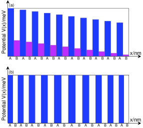
Fig. 1 shows the system of BLG GSLs. In Fig. 1(a), we introduce a gradient in the potential height of higher barriers (A) and lower barriers (B) by decreasing per period. Here, A (B) denotes alternating barriers with the widths . A period contains and . At the th period, the potentials with coordinate can be expressed briefly as = when and = when , where , is the number of period and =. In Fig. 1(b), we introduce a gradient in the widths of barriers (A) and wells (B) while keeping other parameters constant. In the same period, the width of barrier and well is the same. At th period, the width of barrier (or well) is = when , and = when . Here the potential structure is symmetric so =. As one will see in Fig. 6, this specific structure can make an interesting and symmetric band structure.
We consider the one-particle Hamiltonian for BLG
| (1) |
where is the electrostatic potential, is the interlayer coupling, the momentum operators , , m/s is the Fermi velocity. This Hamiltonian satisfies the eigenequation =, where is a four-component spinors . Due to the translation invariance in the direction, the wave function can be rewritten as , . The solution of eigenequation leads to a transfer matrix
| (2) |
which connects the wave function at any two points inside the th potential, and
| (3) |
Here =, =, =, , and =. The entire transfer matrix = is for the whole structure. We also get the reflection coefficient = and the transmission coefficient =
| (4) |
| (5) |
is the element of total transfer matrix . Meanwhile, if we define a matrix as
| (6) |
here is the width in the th potential and the matrix denotes the transport of particles in the direction. So the wave functions at any coordinate
| (7) | |||||
where =1,2,3,4 and are the elements of matrix .
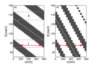
It is conveniently to calculate the band structures, transmission spectrum and reflection coefficient by transfer matrix methodLGWang2010 . Fig. 2 represents the trace maps for two situations with the change of the depth in the system shown as Fig.1(a). One can see that the minibands (white) and minigaps (gray) incline under the external inclined potential, which implies that the band edges depend linearly on the depth of sample. The trace maps becomes titling, thus the occurrence of BO becomes possible. In Fig. 2(a), the white line in bandgap denotes the central position of zero- gapCL2013 , and we highlight two regions called region I and region II using two adjacent horizonal lines. EBO usually takes place in these regions, so we call them Bloch zone. Certainly, there shall be a general condition for such occurrence of BO, which will be discussed latter. Compared with Fig. 2(a), a larger makes the structure more tilting and the two Bloch zones overlap. Assuming that an electron with energy of 75meV, as the red arrows show, it will oscillate in the left band. Because of the overlap of the Bloch zone, electrons may resonant tunnel from the left miniband to the right and oscillate in the right band, which is called Zener tunneling. Thus, Bloch-Zener oscillation takes place. We could have a better understanding of this phenomenon with transmission spectrum in Fig. 3.
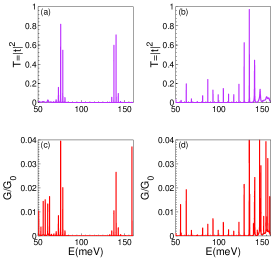
Figs. 3(a) and (b) show the behavior of transmission spectrums. From Figs. 3(a), one can see that there are several transmission peaks equally spaced by , which demonstrates the formation of WSLs, but electrons are totally reflected when the incident energy is outside of the Bloch zone. Conductance is a remarkable transport factorSDatta1995 ; TXMa2012 ; CL2013 , which are plotted in Figs. 3(c) and (d), corresponding to Figs. 2(a) and (b), respectively. Obviously, shows equally spaced peaks and the positions of these peaks are the same with transmission spectrum in Figs. 3(a) and (b). In Figs. 3(b) and (d), one can clearly see that Bloch-Zener oscillation occur even though the BO takes the main part because electrons can transmit at the whole energy range. The main parameter ruling the dynamics of BO is the oscillation period , where is the Plank constant. The shown in Figs. 3(a) and (b) is 1.64ps and 0.69ps, respectively. Their oscillation frequencies, locate at terahertz.
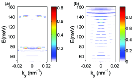
WSLs, with an energy separation between adjacent resonance, are frequency domain counterpart of BO. BO is quantum-interference phenomenon involving Wannier-Stark statesHK1996 . As one can see, WSLs are seen as colorized horizonal lines equally spaced with in Figs. 4(a) and (b), and their positions are corresponding to the transmission peaks in Fig. 3 greatly. Here WSLs are also direct evidence for the occurrence of BO. Moreover, the transmission values vary with in Fig. 4, which means transmission spectrum is sensitive to the incident angles. The transmission value takes maximum value when electrons are at normal incident.
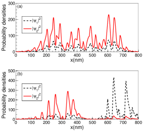
In Figs. 5(a) and (b), we plot the wave functions defined by Eq. 7, corresponding to Figs. 2(a) and (b), respectively. We find that and ( and ) have the same values because of the symmetry of Hamiltonian. The incident energy of electrons in Fig. 5(a)matches one of the transmission peaks in Fig. 3(a) rather well. Fig. 5 (a) demonstrates that wave functions are highly localized from 100nm to 700nm, which corresponds to Fig. 2(a) perfectly. The localized wave functions means electrons oscillate at this region. Intriguingly, the wave functions localize at two parts of the system, see Fig. 5(b). This can be explained by the effect of Bloch-Zener oscillation.
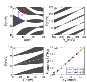
Finding a general condition to control the BO is more useful. In Fig. 6(a), we define the zero- gap as the center and label the gap (G denotes its width) and minibands(B denotes its width) from center in order. Combining with Fig. 2, the general condition for occurrence of BO can be expressed as . For Bloch-Zener oscillation, it is . Thus one can control the occurrence of BO by adjusting the number of period or the gradient of potential . But the width of minibands and gaps is dominated by several parameters such as potential values and barrier’s width and interlayer coupling. Fig. 6(a) shows the width of gaps and minibands highly depend on the barriers’ widths, and Figs. 6(b) and 6(c) show the effect of potential values and , respectively.
The domain parameter in BO mechanic is the frequency and we study the effect of and on in Fig. 6(d). It is obvious that decreases linearly as increases, which provides a proper way to control the Bloch frequency. A much larger is necessary for the developing of BO as the gaps become larger with a larger , which is helpful for the reflection of electron at the boundary of minibands.
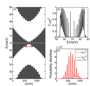
In another system shown as Fig. 1(b), BO can also emerge. In the vicinity of zero- gap shown as white horizonal line in Fig. 7(a), system has robust transport properties. The band structure is symmetric and changes non-linearly with depth of sample, but the zero- gap stays at the same position. There is also a Bloch zone at 60-80meV. Different from the transmission spectrum in Fig. 3, the distance between the peaks in Fig. 7(b) is not the same. Wave functions localize at some special regions shown as Fig. 7(c), which coincides perfectly with the band structure, as the red arrows shown in Fig. 7(a).
In summary, EBO and Bloch-Zener oscillation in two kinds of BLG GSLs are investigated. It is found that terahertz BO and WSLs can be generated in BLG GSLs. In our systems, the band structures are spatially titling and separated by gaps. WSLs appear as a series of equally spaced transmission peaks. By changing the potential’s gradient (height or width), BO’s period can be tunable linearly. Our proposal is in principle possible realized by time-resolved electro-optic techniqueTD1994 ; MH1999 ; YS2004 . These results may be important to the applications in graphene-based electronicsMB2009 ; GJ2011 ; LK2012 ; ED2014 .
T. Ma thanks CAEP for partial financial support. This work is supported by NSFCs (Grant. Nos. 11104014, 11374034, 11274275, and 61078021), and the National Basic Research Program of China (Grant Nos. 2011CBA00108, and 2012CB921602). Hemeng Cheng and Changan Li contributed equally to this work.
References
- (1) F. Bloch, Z. Phys. 52,555 (1928); C. Zener, Proc. R. Soc. London A 145 523 (1934).
- (2) N. Sekine, and K. Hirakawa, Phys. Rev. Lett. 94, 057408 (2005).
- (3) R. Sapienza, P. Costantino, D. Wiersma, M. Ghulinyan, C. J. Oton, and L. Pavesi, Phys. Rev. Lett. 91, 263902 (2009).
- (4) G. Malpuech, A. Kavokin, G. Panzarini and A. Di Carlo, Phys. Rev. B 63, 035108 (2001).
- (5) A. Vojvodica, A. Bloma, Z. Ma, Y. Shimadac, K. Hirakawac, K. A. Chaoa, Solid State Communications 136, 580(2005).
- (6) A. G. Chynoweth, G. H. Wannier, R. A. Logan, and D. E. Thomas Phys. Rev. Lett. 5, 57 (1960).
- (7) K. Leo, Peter H. Bolivar, F. Brüggemann, R. Schwedler, Solid State Commun. 84, 943 (1992).
- (8) C. Waschke, H. G. Roskos, R. Schwedler, K. Leo, H. Kurz, and K. Köhler, Phys. Rev. Lett. 70, 3319 (1993).
- (9) J. Feldmann, K. Leo, J. Shah, D. A. B. Miller, J. E. Cunningham, T. Meier, G. von Plessen, A. Schulze, P. Thomas, and S. Schmitt-Rink, Phys. Rev. B 46, 7252 (1992).
- (10) J. C. Meyer, C. O. Girit, M. F. Crommite and A. Zettl, Appl. Phys. Lett. 92,123110 (2008).
- (11) A. L. Vazquez de Parga, F. Calleja, B. Borca, M. C. G. Passeggi, J. J. Hinarejos, F. Guinea, and R. Miranda, Phys. Rev. Lett. 100, 056807 (2008).
- (12) C.-H. Park, L. Yang, Y.-W. Son, M. L. Cohen, and S. G. Louie, Nat. Phys. 4, 213 (2008).
- (13) T. Ma, C. Liang, L.-G Wang, and Hai-Qing Lin, Appl. Phys. Lett. 100, 252402 (2012).
- (14) L. Z. Tan, C.-H Park, and S. G. Louie, Nano Lett. 11, 2596 (2011).
- (15) L.-G. Wang and S.-Y. Zhu, Phys. Rev. B 81, 205444 (2010).
- (16) M. Barbier, P. Vasilopoulos, F. M. Peeters, and J. M. Pereira, Phys. Rev. B 79, 155402 (2009); M. Barbier, P. Vasilopoulos, and F. M. Peeters, Phys. Rev. B 82, 235408 (2010).
- (17) G. J. Ferreira, M. N. Leuenberger, D. Loss, and J. C. Egues, Phys. Rev. B 84, 125453 (2011).
- (18) L.-K. Lim, J.-N. Fuchs, and G. Montambaux, Phys. Rev. Lett. 108, 175303 (2012).
- (19) E. Díaz, K. Miralles, F. Domílnguez-Adame, and C. Gaul, arXiv:1407.0651v1.
- (20) D. Dragoma and M. Dragoman, Appl. Phys. Lett. 93, 103105 (2008).
- (21) V. Krueckl, and K. Richter, Phys. Rev. B 85, 115433 (2012).
- (22) Andrey R. Kolovsky, and Evgeny N. Bulgakov, Phys. Rev. A 87, 033602 (2013).
- (23) K. S. Novoselov, A. K. Geim, S. V. Morozov, D. Jiang, M. I. Katsnelson, I. V. Grigorieva, S. V. Dubonos and A. A. Firsov, Nature 438, 197 (2005).
- (24) Y. Zhang, Y. W. Tan, H. L. Stormer, and P.Kim, Nature 438, 201 (2005).
- (25) L. L. Bonilla, M. Álvaro, and M. Carretero, Phys. Rev. B 84, 155316 (2011).
- (26) K. Leo, High-Field Transport in Semiconductor Superlattices, Springer Tracts in Modern Physics 187 (Springer, Berlin, 2003).
- (27) M. Killi, S. Wu, and A. Paramekanti, Phys. Rev. Lett. 107, 086801 (2011).
- (28) C. Li, H. Cheng, R. Chen, T. Ma, L.-G. Wang, Y. Song, H.-Q. Lin, Appl. Phys. Lett. 103, 172106 (2013).
- (29) S. Datta, Electronic Transport in Mesoscopic Systems (Cambridge University Press, Cambridge, England, 1995).
- (30) H. Kurz, H. G. Roskos, T. Dekorsy, and K. Kohler, Phil. Trans. R. Soc. Lon. A 354, 2295 (1996).
- (31) T. Dekorsy, P. Leisching, K. Kohler, and H. Kurz, Phys. Rev. B 50, 8160 (1994).
- (32) M. Helm, W. Hilber, G. Strasser, R. De Meester, F. M. Peeters, and A. Wacker, Phys. Rev. Lett. 82, 3120 (1999).
- (33) Y. Shimada, N. Sekine, and K. Hirakawa, Appl. Phys. Lett. 84, 4926 (2004).