AA-stacked bilayer graphene in an applied electric field: Tunable antiferromagnetism and coexisting exciton order parameter

R.S. Akzyanov Moscow Institute of Physics and Technology, Dolgoprudny, Moscow Region, 141700 Russia Institute for Theoretical and Applied Electrodynamics, Russian Academy of Sciences, Moscow, 125412 Russia All-Russia Research Institute of Automatics, Moscow, 127055 Russia    A.O. Sboychakov Institute for Theoretical and Applied Electrodynamics, Russian Academy of Sciences, Moscow, 125412 Russia CEMS, RIKEN, Saitama, 351-0198, Japan    A.V. Rozhkov Moscow Institute of Physics and Technology, Dolgoprudny, Moscow Region, 141700 Russia Institute for Theoretical and Applied Electrodynamics, Russian Academy of Sciences, Moscow, 125412 Russia CEMS, RIKEN, Saitama, 351-0198, Japan    A.L. Rakhmanov Moscow Institute of Physics and Technology, Dolgoprudny, Moscow Region, 141700 Russia Institute for Theoretical and Applied Electrodynamics, Russian Academy of Sciences, Moscow, 125412 Russia All-Russia Research Institute of Automatics, Moscow, 127055 Russia CEMS, RIKEN, Saitama, 351-0198, Japan    Franco Nori CEMS, RIKEN, Saitama, 351-0198, Japan Department of Physics, University of Michigan, Ann Arbor, MI 48109-1040, USA
Abstract

We study the electronic properties of AA-stacked bilayer graphene in a transverse electric field. The strong on-site Coulomb repulsion stabilizes the antiferromagnetic order in such a system. The antiferromagnetic order is suppressed by the transverse bias voltage, at least partially. The inter-plane Coulomb repulsion and non-zero voltage stabilize an exciton order parameter. The exciton order parameter coexists with the antiferromagnetism and can be as large as several tens of meV for realistic values of the bias voltage and interaction constants. The application of a transverse bias voltage can be used to control the transport properties of the bilayer.

pacs:
73.22.Pr, 73.22.Gk, 73.21.Ac

I Introduction

The electronic properties of graphene are a subject of active theoretical and experimental studies Castro Neto et al. (2009); Abergel et al. (2010); Rozhkov et al. (2011). In addition to single-layer graphene, bilayer graphene also attracts significant research attention. This interest is partly driven by the desire to extend the family of graphene-like materials, and to create materials with a controllable gap in the electronic spectrum.

The most studied form of bilayer is the AB (or Bernal) stacked bilayer graphene (AB-BLG) McCann and Fal’ko (2006); Feldman et al. (2009); ABBLG ; Mayorov et al. (2011); aleiner . The biased AB-BLG has a tunable gap biased_ab ; Zhang_ab . Excitons can exist in the AB-BLG under certain conditions Fukidome2014 ; Nano_exciton .

The AA-stacked bilayer graphene (AA-BLG) has received less attention de Andres et al. (2008); Prada et al. (2011); Chiu et al. (2010); Ho et al. (2010); aa first ; Liu et al. (2009); Borysiuk et al. (2011); our_preprint ; Last_paper ; our_preprint2 . However, samples of AA-BLG have recently been produced Liu et al. (2009); Borysiuk et al. (2011); aa first and a detailed study of this system becomes necessary. A significant feature of the AA-BLG is the perfect nesting of the hole and electron Fermi surfaces. These degenerate Fermi surfaces are unstable with respect of an arbitrarily weak electron interaction, and the AA-BLG becomes an antiferromagnetic (AFM) insulator with a finite electron gap our_preprint . This electronic instability is strongest at zero doping, when the bands cross at the Fermi level.

An interesting phenomenon, which occurs in bilayer graphene systems, is exciton condensation Eisenstein_nature ; Coulomb_drag . In graphene bilayers, exciton condensation attracted attention for both fundamental reasons Joglekar ; Min ; Perali ; Rossi ; Sokolik and possible applications in devices, including ultra-fast switches and dispersionless field-effect transistors BISFET .

The purpose of this paper is to investigate the influence of a transverse electric field on the properties of the AA-BLG. We show that such a field can partially suppress the AFM order parameter. However, the degree of suppression heavily depends on the effective value of the on-site Coulomb repulsion. Moreover, the transverse bias stabilizes the exciton order parameter. Namely, we found that the exciton order parameter coexists with the AFM order if a transverse electric field is applied. The exciton order is tuned by the voltage and tied to the AFM order. Since the magnitude of the gap is sensitive to the transverse field, it appears possible to control the transport properties of the bilayer with the help of a transverse bias, which can be created by, e.g., a gate electrode.

The paper is organized as follows. In section II we analyze the single-electron part of our model. Within the tight-binding approach we derive the degenerate electronic spectrum of the model. In section III we consider the on-site and inter-site inter-plane Coulomb repulsion using a mean-field theory. The electronic interaction removes the degeneracy of the single electron spectrum creating a gap. We found that the phase with coexisting AFM and exciton orders is the most stable one. We obtain the equations for the order parameters and solve them using both analytic and numerical methods.

Refer to caption
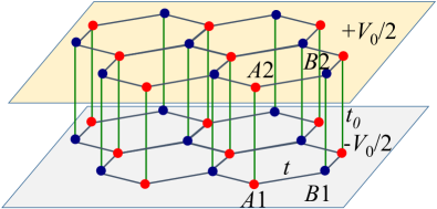
Figure 1: (Color online) Crystal structure of the AA-stacked bilayer graphene. The circles denote carbon atoms in the 𝒜𝒜{\cal A} (red) and {\cal B} (blue) sublattices in the bottom (1), in grey, and top (2), in yellow, layers. The unit cell of the AA-BLG consists of four atoms A1𝐴1A1, A2𝐴2A2, B1𝐵1B1, and B2𝐵2B2. The hopping integrals t𝑡t and t0subscript𝑡0t_{0} correspond to the in-plane and inter-plane nearest-neighbor hopping. A transverse electrical voltage V0subscript𝑉0V_{0} is applied to the planes.

II Tight-binding Hamiltonian

The crystal structure of the AA-BLG is shown in Fig. 1. The AA-BLG consists of two graphene layers, 111 and 222. Each carbon atom of the upper layer is located above the corresponding atom of the lower layer. Each layer consists of two triangular sublattices 𝒜𝒜{\cal A} and {\cal B}. The elementary unit cell of the AA-BLG contains four carbon atoms A1𝐴1A1, A2𝐴2A2, B1𝐵1B1, and B2𝐵2B2.

We write the single-particle tight-binding Hamiltonian of the AA-BLG in the form

H0subscript𝐻0\displaystyle H_{0} =\displaystyle= t𝐧𝐦iσ(d𝐧i𝒜σd𝐦iσ+H.c.)+\displaystyle-t\sum_{\langle\mathbf{nm}\rangle i\sigma}\left(d^{{\dagger}}_{\mathbf{n}i{\cal A}\sigma}d^{\phantom{{\dagger}}}_{\mathbf{m}i{\cal B}\sigma}+H.c.\right)+
t0𝐧aσ(d𝐧1aσd𝐧2aσ+H.c.)+\displaystyle t_{0}\sum_{\mathbf{n}a\sigma}\left(d^{{\dagger}}_{\mathbf{n}1a\sigma}d^{\phantom{{\dagger}}}_{\mathbf{n}2a\sigma}+H.c.\right)+
V02𝐧aσ(d𝐧1aσd𝐧1aσd𝐧2aσd𝐧2aσ).subscript𝑉02subscript𝐧𝑎𝜎subscriptsuperscript𝑑𝐧1𝑎𝜎subscriptsuperscript𝑑absent𝐧1𝑎𝜎subscriptsuperscript𝑑𝐧2𝑎𝜎subscriptsuperscript𝑑absent𝐧2𝑎𝜎\displaystyle\frac{V_{0}}{2}\sum_{\mathbf{n}a\sigma}\left(d^{{\dagger}}_{\mathbf{n}1a\sigma}d^{\phantom{{\dagger}}}_{\mathbf{n}1a\sigma}-d^{{\dagger}}_{\mathbf{n}2a\sigma}d^{\phantom{{\dagger}}}_{\mathbf{n}2a\sigma}\right).

Here d𝐧iaσsubscriptsuperscript𝑑𝐧𝑖𝑎𝜎d^{{\dagger}}_{\mathbf{n}ia\sigma} and d𝐧iaσsubscriptsuperscript𝑑absent𝐧𝑖𝑎𝜎d^{\phantom{{\dagger}}}_{\mathbf{n}ia\sigma} are the creation and annihilation operators of an electron with spin projection σ𝜎\sigma in the layer i=1,2𝑖12i=1,2 on the sublattice a=𝒜,𝑎𝒜a={\cal A},{\cal B} at the position 𝐧𝐧\mathbf{n}, and delimited-⟨⟩\langle...\rangle denotes a nearest-neighbor pair inside a layer. The amplitude t𝑡t (t0subscript𝑡0t_{0}) in Eq. (II) describes the in-plane (inter-plane) nearest-neighbor hopping, V0subscript𝑉0V_{0} is the voltage applied perpendicular to the layers. We assume that V0tmuch-less-thansubscript𝑉0𝑡V_{0}\ll t, which corresponds to typical experimental conditions biased_ab ; Zhang_ab . For calculations, we use the values of the hopping integrals t=2.57𝑡2.57t=2.57 eV, t0=0.36subscript𝑡00.36t_{0}=0.36 eV, computed by the DFT method for multilayer carbon systems in Ref. Charlier et al., 1992.

After diagonalizing the Hamiltonian (II) we obtain four bands ε0𝐤(s)subscriptsuperscript𝜀𝑠0𝐤\varepsilon^{(s)}_{0\mathbf{k}} (s=1,,4𝑠14s=1,\dots,4), which can be written as

ε0𝐤(1)=t02+V024tζ𝐤,ε0𝐤(2)=t02+V024+tζ𝐤,formulae-sequencesubscriptsuperscript𝜀10𝐤superscriptsubscript𝑡02superscriptsubscript𝑉024𝑡subscript𝜁𝐤subscriptsuperscript𝜀20𝐤superscriptsubscript𝑡02superscriptsubscript𝑉024𝑡subscript𝜁𝐤\displaystyle\varepsilon^{(1)}_{0\mathbf{k}}=-\sqrt{t_{0}^{2}+\frac{V_{0}^{2}}{4}}-t\zeta_{\bf k}\,,\,\,\varepsilon^{(2)}_{0\mathbf{k}}=-\sqrt{t_{0}^{2}+\frac{V_{0}^{2}}{4}}+t\zeta_{\bf k}\,,
ε0𝐤(3)=t02+V024tζ𝐤,ε0𝐤(4)=t02+V024+tζ𝐤,formulae-sequencesubscriptsuperscript𝜀30𝐤superscriptsubscript𝑡02superscriptsubscript𝑉024𝑡subscript𝜁𝐤subscriptsuperscript𝜀40𝐤superscriptsubscript𝑡02superscriptsubscript𝑉024𝑡subscript𝜁𝐤\displaystyle\varepsilon^{(3)}_{0\mathbf{k}}=\sqrt{t_{0}^{2}+\frac{V_{0}^{2}}{4}}-t\zeta_{\bf k}\,,\,\,\,\,\,\varepsilon^{(4)}_{0\mathbf{k}}=\sqrt{t_{0}^{2}+\frac{V_{0}^{2}}{4}}+t\zeta_{\bf k}\,, (2)

where

ζ𝐤=|f𝐤|,f𝐤=1+2exp(3ikxa02)cos(3kya02),formulae-sequencesubscript𝜁𝐤subscript𝑓𝐤subscript𝑓𝐤123𝑖subscript𝑘𝑥subscript𝑎023subscript𝑘𝑦subscript𝑎02\zeta_{\bf k}=|f_{\bf k}|\,,\;\;f_{\mathbf{k}}\!=\!1+2\exp\!\left(\frac{3ik_{x}a_{0}}{2}\right)\cos\!\left(\!\!\frac{\sqrt{3}k_{y}a_{0}}{2}\!\!\right), (3)

and a0=1.42subscript𝑎01.42a_{0}=1.42 Å is the in-plane carbon-carbon distance. The bands s=2𝑠2s=2 and s=3𝑠3s=3 cross the Fermi level near the Dirac points 𝐊=2π(3, 1)/(33a0)𝐊2𝜋3133subscript𝑎0\mathbf{K}=2\pi(\sqrt{3},\,1)/(3\sqrt{3}a_{0}) and 𝐊=2π(3,1)/(33a0)superscript𝐊2𝜋3133subscript𝑎0\mathbf{K}^{\prime}=2\pi(\sqrt{3},\,-1)/(3\sqrt{3}a_{0}). As it follows from Eqs. (II), the band s=2𝑠2s=2 is electron-like, while the band s=3𝑠3s=3 is hole-like. The band s=1𝑠1s=1 lies below and the band s=4𝑠4s=4 lies above the Fermi energy and, consequently, they do not form a Fermi surface.

In contrast to the Bernal stacking (where the bias voltage opens a gap at the Fermi level biased_ab ; Zhang_ab ), the application of a transverse bias voltage does not qualitatively change the spectrum of the AA-BLG. The Fermi surface is given by the equation ζ𝐤=t1t02+V02/4=ζ0subscript𝜁𝐤superscript𝑡1superscriptsubscript𝑡02superscriptsubscript𝑉024subscript𝜁0\zeta_{\bf k}=t^{-1}\sqrt{t_{0}^{2}+V_{0}^{2}/4}=\zeta_{0}. Since ζ01much-less-thansubscript𝜁01\zeta_{0}\ll 1, we can expand the function ζ𝐤subscript𝜁𝐤\zeta_{\bf k} near the Dirac points and find that the Fermi surface consists of two circles with radius kr=2ζ0/(3a0)subscript𝑘𝑟2subscript𝜁03subscript𝑎0k_{r}=2\zeta_{0}/(3a_{0}).

One of the most important features of this tight-binding band structure is that the Fermi surfaces of both bands coincide. That is, the electron and hole components of the Fermi surface are perfectly nested. This property of the Fermi surface is quite robust against changes in the tight-binding Hamiltonian. It survives even if longer-range hoppings are taken into account, or a system with two non-equivalent layers is considered (e.g., the single-side hydrogenated graphene sshg ). However, the electron interactions can remove the degeneracy in the spectrum, creating a finite gap our_preprint .

III Electron-electron interaction

The electronic spectrum changes drastically when considering the Coulomb interaction. To study the effects of this interaction on the electronic properties of our system, we use the following Hubbard-like Hamiltonian

Hint=HU+HV.subscript𝐻intsubscript𝐻Usubscript𝐻VH_{\textrm{int}}=H_{\textrm{U}}+H_{\textrm{V}}\,. (4)

The first term, HUsubscript𝐻UH_{\textrm{U}}, is the on-site Coulomb repulsion between the electrons,

HU=U0𝐧ia(n𝐧ia12)(n𝐧ia12),subscript𝐻Usubscript𝑈0subscript𝐧𝑖𝑎subscript𝑛𝐧𝑖𝑎absent12subscript𝑛𝐧𝑖𝑎absent12H_{\textrm{U}}=U_{0}\sum_{\mathbf{n}ia}\left(n_{\mathbf{n}ia\uparrow}-\frac{1}{2}\right)\!\!\left(n_{\mathbf{n}ia\downarrow}-\frac{1}{2}\right)\,, (5)

where n𝐧iaσ=d𝐧iaσd𝐧iaσsubscript𝑛𝐧𝑖𝑎𝜎subscriptsuperscript𝑑𝐧𝑖𝑎𝜎subscriptsuperscript𝑑absent𝐧𝑖𝑎𝜎n_{\mathbf{n}ia\sigma}=d^{{\dagger}}_{\mathbf{n}ia\sigma}d^{\phantom{{\dagger}}}_{\mathbf{n}ia\sigma} is the operator of the occupation number. The second term, HVsubscript𝐻VH_{\textrm{V}}, describes the nearest-neighbor Coulomb repulsion. It has a form

HVsubscript𝐻V\displaystyle H_{\textrm{V}} =\displaystyle= U12𝐧aσσ(n𝐧1aσ12)(n𝐧2aσ12)+limit-fromsubscript𝑈12subscriptFRACOP𝐧𝑎𝜎superscript𝜎subscript𝑛𝐧1𝑎𝜎12subscript𝑛𝐧2𝑎superscript𝜎12\displaystyle U_{12}\sum_{\scriptstyle\mathbf{n}a\atop\scriptstyle\sigma\sigma^{\prime}}\left(n_{\mathbf{n}1a\sigma}-\frac{1}{2}\right)\!\!\left(n_{\mathbf{n}2a\sigma^{\prime}}-\frac{1}{2}\right)+ (6)
Uab𝐧𝐦iσσ(n𝐧i𝒜σ12)(n𝐦iσ12),subscript𝑈𝑎𝑏subscriptFRACOPdelimited-⟨⟩𝐧𝐦𝑖𝜎superscript𝜎subscript𝑛𝐧𝑖𝒜𝜎12subscript𝑛𝐦𝑖superscript𝜎12\displaystyle U_{ab}\!\sum_{\scriptstyle\langle\mathbf{nm}\rangle\atop\scriptstyle i\sigma\sigma^{\prime}}\left(n_{\mathbf{n}i{\cal A}\sigma}-\frac{1}{2}\right)\!\!\left(n_{\mathbf{m}i{\cal B}\sigma^{\prime}}-\frac{1}{2}\right)\!,

where the first term is the nearest-neighbor interaction between the electrons in different layers, while the second term describes the in-plane nearest-neighbor interaction. The terms 1/2121/2 in the brackets in Eqs. (5) and (6) are added to keep the chemical potential corresponding to the half-filling (zero doping) equal to zero.

The value of the electron-electron interaction in graphene is relatively strong. According to DFT calculations U69 , the on-site repulsion energy, U0subscript𝑈0U_{0}, is about 9–10 eV, while the in-plane inter-site repulsion, Uabsubscript𝑈𝑎𝑏U_{ab}, is about 5–6 eV. The nearest-neighbor inter-plane interaction in the bilayer graphene is unknown. We can estimate it as U12Uaba0/c2.5subscript𝑈12subscript𝑈𝑎𝑏subscript𝑎0𝑐2.5U_{12}\approx U_{ab}\,a_{0}/c\approx 2.5 eV, where c=3.35𝑐3.35c=3.35 Å is the distance between the layers. It is commonly accepted that the mean-field calculations overestimate the resulting value of the antiferromagnetic (AFM) order parameter driven by the electron-electron interaction. In addition, the long range Coulomb interaction can effectively reduce Effective_onsite the on-site repulsion energy U0subscript𝑈0U_{0}. Keeping all this in mind, we use for further estimates the values of U0subscript𝑈0U_{0}, Uabsubscript𝑈𝑎𝑏U_{ab}, and U12subscript𝑈12U_{12} smaller than those obtained in the DFT calculations. We will use U0/tsimilar-to-or-equalssubscript𝑈0𝑡absentU_{0}/t\simeq2–3.5, Uab/tsimilar-to-or-equalssubscript𝑈𝑎𝑏𝑡absentU_{ab}/t\simeq1–2, and U12/tsimilar-to-or-equalssubscript𝑈12𝑡absentU_{12}/t\simeq0.5–1.

III.1 Mean-field equations

We analyze the properties of the total Hamiltonian H=H0+Hint𝐻subscript𝐻0subscript𝐻intH=H_{0}+H_{\textrm{int}} in the mean-field approximation. It was shown previously for zero bias voltage that the on-site Coulomb repulsion stabilizes the AFM ground state in the AA-BLG our_preprint ; Last_paper ; our_preprint2 . We will show below that the AFM order also exists for V00subscript𝑉00V_{0}\neq 0. We fix the spin quantization z𝑧z-axis perpendicular to the layers in the xy𝑥𝑦xy plane. In this case the AFM order parameter can be written as

ΔAFMia=U02(d𝐧iad𝐧iad𝐧iad𝐧ia),superscriptsubscriptΔAFM𝑖𝑎subscript𝑈02delimited-⟨⟩subscriptsuperscript𝑑𝐧𝑖𝑎absentsubscriptsuperscript𝑑absent𝐧𝑖𝑎absentdelimited-⟨⟩subscriptsuperscript𝑑𝐧𝑖𝑎absentsubscriptsuperscript𝑑absent𝐧𝑖𝑎absent\displaystyle\Delta_{\textrm{AFM}}^{ia}=\frac{U_{0}}{2}\left(\left\langle d^{{\dagger}}_{\mathbf{n}ia\uparrow}d^{\phantom{{\dagger}}}_{\mathbf{n}ia\uparrow}\right\rangle-\left\langle d^{{\dagger}}_{\mathbf{n}ia\downarrow}d^{\phantom{{\dagger}}}_{\mathbf{n}ia\downarrow}\right\rangle\right)\,, (7)
ΔAFM1𝒜=ΔAFM2=ΔAFM1=ΔAFM2𝒜ΔAFM,superscriptsubscriptΔAFM1𝒜superscriptsubscriptΔAFM2superscriptsubscriptΔAFM1superscriptsubscriptΔAFM2𝒜subscriptΔAFM\displaystyle\Delta_{\textrm{AFM}}^{1\cal{A}}=\Delta_{\textrm{AFM}}^{2\cal{B}}=-\Delta_{\textrm{AFM}}^{1\cal{B}}=-\Delta_{\textrm{AFM}}^{2\cal{A}}\equiv\Delta_{\textrm{AFM}}\,, (8)

and the ΔAFMsubscriptΔAFM\Delta_{\textrm{AFM}} is real. Such an AFM order, when the spin at any given site is antiparallel to spins at all its nearest-neighbor sites, is referred as G-type AFM. In the mean-field approximation, the on-site interaction Hamiltonian, HUsubscript𝐻UH_{\text{U}}, takes the form

HUMFsubscriptsuperscript𝐻MFU\displaystyle H^{\rm MF}_{\text{U}}\!\! =\displaystyle= 𝒩U0Δn24+U0Δn4𝐧aσ(n𝐧1aσn𝐧2aσ)+𝒩subscript𝑈0Δsuperscript𝑛24limit-fromsubscript𝑈0Δ𝑛4subscript𝐧𝑎𝜎subscript𝑛𝐧1𝑎𝜎subscript𝑛𝐧2𝑎𝜎\displaystyle\!-\frac{{\cal N}U_{0}\Delta n^{2}}{4}+\frac{U_{0}\Delta n}{4}\sum_{\mathbf{n}a\sigma}\left(n_{\mathbf{n}1a\sigma}-n_{\mathbf{n}2a\sigma}\right)+ (9)
4𝒩ΔAFM2U0𝐧iaΔAFMia(n𝐧ian𝐧ia),4𝒩superscriptsubscriptΔAFM2subscript𝑈0subscript𝐧𝑖𝑎superscriptsubscriptΔAFM𝑖𝑎subscript𝑛𝐧𝑖𝑎absentsubscript𝑛𝐧𝑖𝑎absent\displaystyle\frac{4{\cal N}\Delta_{\textrm{AFM}}^{2}}{U_{0}}-\!\sum_{\mathbf{n}ia}\!\Delta_{\textrm{AFM}}^{ia}\!\left(n_{\mathbf{n}ia\uparrow}-n_{\mathbf{n}ia\downarrow}\!\right)\!,

where Δn=σ(n𝐧1aσn𝐧2aσ)Δ𝑛subscript𝜎delimited-⟨⟩subscript𝑛𝐧1𝑎𝜎delimited-⟨⟩subscript𝑛𝐧2𝑎𝜎\Delta n=\sum_{\sigma}(\langle n_{\mathbf{n}1a\sigma}\rangle-\langle n_{\mathbf{n}2a\sigma}\rangle) is the difference in the electron densities in two graphene layers induced by the applied voltage V0subscript𝑉0V_{0} and 𝒩𝒩{\cal N} is the number of unit cells in the sample.

Let us consider now the inter-site part of the interaction. The Hamiltonian HVsubscript𝐻VH_{\text{V}} can produce several order parameters in the system. However, for zero-bias voltage all of them compete with the antiferromagnetism and only the antiferromagnetic order parameter survives, because U0subscript𝑈0U_{0} is the strongest interaction constant. A nonzero bias voltage breaks the symmetry between two graphene layers. In this case, there exists an order parameter driven by the inter-layer interaction, which coexists with antiferromagnetism. An analysis based on symmetry considerations, similar to that presented in Ref. our_preprint, , shows that this order parameter should have a form

ΔexcasuperscriptsubscriptΔexc𝑎\displaystyle\Delta_{\textrm{exc}}^{a} =\displaystyle= U122(d𝐧1ad𝐧2ad𝐧1ad𝐧2a),subscript𝑈122delimited-⟨⟩subscriptsuperscript𝑑𝐧1𝑎absentsubscriptsuperscript𝑑absent𝐧2𝑎absentdelimited-⟨⟩subscriptsuperscript𝑑𝐧1𝑎absentsubscriptsuperscript𝑑absent𝐧2𝑎absent\displaystyle\frac{U_{12}}{2}\left(\left\langle d^{{\dagger}}_{\mathbf{n}1a\uparrow}d^{\phantom{{\dagger}}}_{\mathbf{n}2a\uparrow}\right\rangle-\left\langle d^{{\dagger}}_{\mathbf{n}1a\downarrow}d^{\phantom{{\dagger}}}_{\mathbf{n}2a\downarrow}\right\rangle\right)\,, (10)
Δexc𝒜superscriptsubscriptΔexc𝒜\displaystyle\Delta_{\textrm{exc}}^{\cal{A}} =\displaystyle= ΔexcΔexc,superscriptsubscriptΔexcsubscriptΔexc\displaystyle-\Delta_{\textrm{exc}}^{\cal{B}}\,\equiv\,\Delta_{\textrm{exc}}\,, (11)

and the ΔexcsubscriptΔexc\Delta_{\textrm{exc}} is real. This order parameter corresponds to the bound state of the electron and the hole in different layers. We call it the exciton order parameter. The mean-field expression for the inter-site part of the Hamiltonian has the following form

HVMFsubscriptsuperscript𝐻MFV\displaystyle H^{\rm MF}_{\textrm{V}}\! =\displaystyle= 𝒩[(3UabU12)Δn22+4Δexc2U12]+limit-from𝒩delimited-[]3subscript𝑈𝑎𝑏subscript𝑈12Δsuperscript𝑛224superscriptsubscriptΔexc2subscript𝑈12\displaystyle\!{\cal N}\left[-\frac{(3U_{ab}-U_{12})\Delta n^{2}}{2}+\frac{4\Delta_{\textrm{exc}}^{2}}{U_{12}}\right]+
(3UabU12)Δn2𝐧aσ(n𝐧1aσn𝐧2aσ)limit-from3subscript𝑈𝑎𝑏subscript𝑈12Δ𝑛2subscript𝐧𝑎𝜎subscript𝑛𝐧1𝑎𝜎subscript𝑛𝐧2𝑎𝜎\displaystyle\frac{(3U_{ab}-U_{12})\Delta n}{2}\sum_{\mathbf{n}a\sigma}\left(n_{\mathbf{n}1a\sigma}-n_{\mathbf{n}2a\sigma}\right)-
𝐧aσ[Δexca(d𝐧1ad𝐧2ad𝐧1ad𝐧2a)+H.c.].\displaystyle\!\sum_{\mathbf{n}a\sigma}\!\left[\Delta_{\textrm{exc}}^{a}\!\left(d^{{\dagger}}_{\mathbf{n}1a\uparrow}d^{\phantom{{\dagger}}}_{\mathbf{n}2a\uparrow}-d^{{\dagger}}_{\mathbf{n}1a\downarrow}d^{\phantom{{\dagger}}}_{\mathbf{n}2a\downarrow}\right)+\!H.c.\!\right]\!.

We introduce the four-component spinor

ψ𝐤σ=(d𝐤1𝒜σ,d𝐤2𝒜σ,d𝐤1σ,d𝐤2σ).subscriptsuperscript𝜓𝐤𝜎subscriptsuperscript𝑑𝐤1𝒜𝜎subscriptsuperscript𝑑𝐤2𝒜𝜎subscriptsuperscript𝑑𝐤1𝜎subscriptsuperscript𝑑𝐤2𝜎\displaystyle\psi^{{\dagger}}_{\mathbf{k}\sigma}=(d^{{\dagger}}_{\mathbf{k}1\cal{A}\sigma},d^{{\dagger}}_{\mathbf{k}2\cal{A}\sigma},d^{{\dagger}}_{\mathbf{k}1\cal{B}\sigma},d^{{\dagger}}_{\mathbf{k}2\cal{B}\sigma})\,. (13)

In terms of this spinor, the mean field Hamiltonian

HMF=H0+HUMF+HVMFsuperscript𝐻MFsubscript𝐻0subscriptsuperscript𝐻MFUsubscriptsuperscript𝐻MFVH^{\rm MF}=H_{0}+H^{\rm MF}_{\rm{U}}+H^{\rm MF}_{\rm{V}} (14)

can be written as

HMF=𝒩E0+𝐤σψ𝐤σ(H^0𝐤+Δ^σ)ψ𝐤σ,superscript𝐻MF𝒩subscript𝐸0subscript𝐤𝜎subscriptsuperscript𝜓𝐤𝜎subscript^𝐻0𝐤subscript^Δ𝜎subscriptsuperscript𝜓absent𝐤𝜎\displaystyle H^{\rm MF}={\cal N}E_{0}+\sum_{\mathbf{k}\sigma}\psi^{{\dagger}}_{\mathbf{k}\sigma}(\hat{H}_{0\mathbf{k}}+\hat{\Delta}_{\sigma})\psi^{\phantom{{\dagger}}}_{\mathbf{k}\sigma}\,, (15)

where E0subscript𝐸0E_{0} is a c𝑐c-number

E0=(U0+6Uab2U12)Δn24+4ΔAFM2U0+4Δexc2U12,subscript𝐸0subscript𝑈06subscript𝑈𝑎𝑏2subscript𝑈12Δsuperscript𝑛244superscriptsubscriptΔAFM2subscript𝑈04superscriptsubscriptΔexc2subscript𝑈12E_{0}=-\frac{(U_{0}+6U_{ab}-2U_{12})\Delta n^{2}}{4}+\frac{4\Delta_{\textrm{AFM}}^{2}}{U_{0}}+\frac{4\Delta_{\textrm{exc}}^{2}}{U_{12}}\,, (16)

and H^0𝐤subscript^𝐻0𝐤\hat{H}_{0\mathbf{k}} and Δ^σsubscript^Δ𝜎\hat{\Delta}_{\sigma} are the 4×4444\times 4 matrices

H^0𝐤=(V/2t0tf𝐤0t0V/20tf𝐤tf𝐤0V/2t00tf𝐤t0V/2),subscript^𝐻0𝐤matrix𝑉2subscript𝑡0𝑡subscript𝑓𝐤0subscript𝑡0𝑉20𝑡subscript𝑓𝐤𝑡superscriptsubscript𝑓𝐤0𝑉2subscript𝑡00𝑡superscriptsubscript𝑓𝐤subscript𝑡0𝑉2\hat{H}_{0\mathbf{k}}=-\left(\begin{matrix}-V/2&t_{0}&tf_{\bf k}&0\cr t_{0}&V/2&0&tf_{\bf k}\cr tf_{\bf k}^{*}&0&-V/2&t_{0}\cr 0&tf_{\bf k}^{*}&t_{0}&V/2\cr\end{matrix}\right)\!, (17)
Δ^=(ΔAFMΔexc00ΔexcΔAFM0000ΔAFMΔexc00ΔexcΔAFM),Δ^=Δ^.formulae-sequencesubscript^ΔmatrixsubscriptΔAFMsubscriptΔexc00subscriptΔexcsubscriptΔAFM0000subscriptΔAFMsubscriptΔexc00subscriptΔexcsubscriptΔAFMsubscript^Δsubscript^Δ\hat{\Delta}_{\uparrow}=\left(\begin{matrix}\Delta_{\textrm{AFM}}&\Delta_{\textrm{exc}}&0&0\cr\Delta_{\textrm{exc}}&-\Delta_{\textrm{AFM}}&0&0\cr 0&0&-\Delta_{\textrm{AFM}}&-\Delta_{\textrm{exc}}\cr 0&0&-\Delta_{\textrm{exc}}&\Delta_{\textrm{AFM}}\cr\end{matrix}\right)\!,\;\hat{\Delta}_{\downarrow}=-\hat{\Delta}_{\uparrow}. (18)

In Eq. (17) the quantity V𝑉V is the effective bias voltage given by the relation

V=V0+αΔn,α=U0+6Uab2U122>0.formulae-sequence𝑉subscript𝑉0𝛼Δ𝑛𝛼subscript𝑈06subscript𝑈𝑎𝑏2subscript𝑈1220V=V_{0}+\alpha\Delta n\,,\,\,\,\;\;\alpha=\frac{U_{0}+6U_{ab}-2U_{12}}{2}>0\,. (19)

This equation describes the screening of the applied voltage due to the electron-electron interaction. Indeed, since Δn<0Δ𝑛0\Delta n<0 for V0>0subscript𝑉00V_{0}>0, we have V<V0𝑉subscript𝑉0V<V_{0}. For the parameters U0subscript𝑈0U_{0}, Uabsubscript𝑈𝑎𝑏U_{ab}, and U12subscript𝑈12U_{12} under study the constant α𝛼\alpha can be estimated as 3.5t𝑡t–7t𝑡t.

The mean-field spectrum is obtained by the diagonalization of two 4×4444\times 4 matrices in Eq. (15). It consists of four bands doubly-degenerate with respect to spin

ε𝐤(1)subscriptsuperscript𝜀1𝐤\displaystyle\varepsilon^{(1)}_{\mathbf{k}} =\displaystyle= A𝐤+2B𝐤,ε𝐤(2)=A𝐤2B𝐤,subscript𝐴𝐤2subscript𝐵𝐤subscriptsuperscript𝜀2𝐤subscript𝐴𝐤2subscript𝐵𝐤\displaystyle-\sqrt{A_{\mathbf{k}}+2B_{\mathbf{k}}}\,,\;\varepsilon^{(2)}_{\mathbf{k}}=-\sqrt{A_{\mathbf{k}}-2B_{\mathbf{k}}}\,,
ε𝐤(3)subscriptsuperscript𝜀3𝐤\displaystyle\varepsilon^{(3)}_{\mathbf{k}} =\displaystyle= A𝐤2B𝐤,ε𝐤(4)=A𝐤+2B𝐤,subscript𝐴𝐤2subscript𝐵𝐤subscriptsuperscript𝜀4𝐤subscript𝐴𝐤2subscript𝐵𝐤\displaystyle\sqrt{A_{\mathbf{k}}-2B_{\mathbf{k}}}\,,\;\;\;\;\varepsilon^{(4)}_{\mathbf{k}}=\sqrt{A_{\mathbf{k}}+2B_{\mathbf{k}}}\,, (20)

where

A𝐤subscript𝐴𝐤\displaystyle A_{\mathbf{k}} =\displaystyle= ΔAFM2+Δexc2+t2ζ𝐤2+t02+V24,superscriptsubscriptΔAFM2superscriptsubscriptΔexc2superscript𝑡2superscriptsubscript𝜁𝐤2superscriptsubscript𝑡02superscript𝑉24\displaystyle\Delta_{\textrm{AFM}}^{2}+\Delta_{\textrm{exc}}^{2}+t^{2}\zeta_{\mathbf{k}}^{2}+t_{0}^{2}+\frac{V^{2}}{4}\,, (21)
B𝐤subscript𝐵𝐤\displaystyle B_{\mathbf{k}} =\displaystyle= [Δexct0+ΔAFMV2]2+t2ζ𝐤2[t02+V24].superscriptdelimited-[]subscriptΔexcsubscript𝑡0subscriptΔAFM𝑉22superscript𝑡2superscriptsubscript𝜁𝐤2delimited-[]superscriptsubscript𝑡02superscript𝑉24\displaystyle\sqrt{\left[-\Delta_{\textrm{exc}}t_{0}+\Delta_{\textrm{AFM}}\frac{V}{2}\right]^{2}+t^{2}\zeta_{\mathbf{k}}^{2}\left[t_{0}^{2}+\frac{V^{2}}{4}\right]}\,.

The full gap in the spectrum ΔΔ\Delta is defined as Δ=min𝐤(ε𝐤(3)ε𝐤(2))Δsubscript𝐤subscriptsuperscript𝜀3𝐤subscriptsuperscript𝜀2𝐤\Delta=\min_{\mathbf{k}}\left(\varepsilon^{(3)}_{\mathbf{k}}-\varepsilon^{(2)}_{\mathbf{k}}\right)/2. It relates to the AFM and exciton order parameters as

Δ=2ΔAFMt0+ΔexcV4t02+V2.Δ2subscriptΔAFMsubscript𝑡0subscriptΔexc𝑉4superscriptsubscript𝑡02superscript𝑉2\displaystyle\Delta=\frac{2\Delta_{\textrm{AFM}}t_{0}+\Delta_{\textrm{exc}}V}{\sqrt{4t_{0}^{2}+V^{2}}}\,. (22)

To determine the values of the order parameters ΔAFMsubscriptΔAFM\Delta_{\textrm{AFM}} and ΔexcsubscriptΔexc\Delta_{\textrm{exc}} we should minimize the grand potential ΩΩ\Omega. The grand potential per unit cell is

Ω=E02Ts=14d𝐤VBZln[1+eε𝐤(s)/T],Ωsubscript𝐸02𝑇superscriptsubscript𝑠14𝑑𝐤subscript𝑉BZ1superscript𝑒subscriptsuperscript𝜀𝑠𝐤𝑇\Omega=E_{0}-2T\!\sum_{s=1}^{4}\!\int\!\frac{d\mathbf{k}}{V_{\text{BZ}}}\ln\left[1+e^{-\varepsilon^{(s)}_{\mathbf{k}}/T}\right]\,, (23)

where VBZsubscript𝑉BZV_{\text{BZ}} is the volume of the first Brillouin zone.

To calculate the integrals over the Brillouin zone, it is convenient to introduce the density of states

ρ0(ζ)=d𝐤VBZδ(ζζ𝐤).subscript𝜌0𝜁𝑑𝐤subscript𝑉BZ𝛿𝜁subscript𝜁𝐤\rho_{0}(\zeta)=\!\int\!\frac{d\mathbf{k}}{V_{\text{BZ}}}\delta(\zeta-\zeta_{\mathbf{k}})\,. (24)

This function is non-zero only if 0<ζ<30𝜁30<\zeta<3. It is related to the single layer graphene density of states ρgr(ζ)subscript𝜌gr𝜁\rho_{\textrm{gr}}(\zeta) as ρgr(ζ)=ρ0(ζ)/tsubscript𝜌gr𝜁subscript𝜌0𝜁𝑡\rho_{\textrm{gr}}(\zeta)=\rho_{0}(\zeta)/t (see Ref. Castro Neto et al., 2009).

Minimization of ΩΩ\Omega with respect to ΔAFMsubscriptΔAFM\Delta_{\textrm{AFM}} and ΔexcsubscriptΔexc\Delta_{\textrm{exc}} gives the equations

4ΔAFMU04subscriptΔAFMsubscript𝑈0\displaystyle\frac{4\Delta_{\textrm{AFM}}}{U_{0}} =\displaystyle= 03𝑑ζρ0(ζ)[ΔAFM+V2θ(ζ)]F(ε(1)(ζ))+limit-fromsuperscriptsubscript03differential-d𝜁subscript𝜌0𝜁delimited-[]subscriptΔAFM𝑉2𝜃𝜁𝐹superscript𝜀1𝜁\displaystyle\int\limits_{0}^{3}\!\!d\zeta\,\rho_{0}(\zeta)\!\!\left[\Delta_{\textrm{AFM}}+\frac{V}{2}\theta(\zeta)\right]\!F\left(\!\varepsilon^{(1)}(\zeta)\!\right)+ (25)
03𝑑ζρ0(ζ)[ΔAFMV2θ(ζ)]F(ε(2)(ζ)),superscriptsubscript03differential-d𝜁subscript𝜌0𝜁delimited-[]subscriptΔAFM𝑉2𝜃𝜁𝐹superscript𝜀2𝜁\displaystyle\!\int\limits_{0}^{3}\!\!d\zeta\,\rho_{0}(\zeta)\!\!\left[\!\Delta_{\textrm{AFM}}-\frac{V}{2}\theta(\zeta)\!\right]\!F\left(\!\varepsilon^{(2)}(\zeta)\!\right),
4ΔexcU124subscriptΔexcsubscript𝑈12\displaystyle\frac{4\Delta_{\textrm{exc}}}{U_{12}} =\displaystyle= 03𝑑ζρ0(ζ)[Δexct0θ(ζ)]F(ε(1)(ζ))+limit-fromsuperscriptsubscript03differential-d𝜁subscript𝜌0𝜁delimited-[]subscriptΔexcsubscript𝑡0𝜃𝜁𝐹superscript𝜀1𝜁\displaystyle\int\limits_{0}^{3}\!\!d\zeta\,\rho_{0}(\zeta)\!\left[\Delta_{\textrm{exc}}-t_{0}\theta(\zeta)\right]F\left(\varepsilon^{(1)}(\zeta)\right)+ (26)
03𝑑ζρ0(ζ)[Δexc+t0θ(ζ)]F(ε(2)(ζ)),superscriptsubscript03differential-d𝜁subscript𝜌0𝜁delimited-[]subscriptΔexcsubscript𝑡0𝜃𝜁𝐹superscript𝜀2𝜁\displaystyle\int\limits_{0}^{3}\!\!d\zeta\,\rho_{0}(\zeta)\!\left[\Delta_{\textrm{exc}}+t_{0}\theta(\zeta)\right]F\left(\varepsilon^{(2)}(\zeta)\right),

where

F(ε)=f(ε)f(ε)ε,f(ε)=1eε/T+1,formulae-sequence𝐹𝜀𝑓𝜀𝑓𝜀𝜀𝑓𝜀1superscript𝑒𝜀𝑇1\displaystyle F(\varepsilon)=\frac{f(-\varepsilon)-f(\varepsilon)}{\varepsilon},\;\;\;\,f(\varepsilon)=\frac{1}{e^{{\scriptstyle\varepsilon}/{\scriptstyle T}}+1}\,,
θ(ζ)=2Δexct0ΔAFMV(2Δexct0ΔAFMV)2+t2(4t02+V2)ζ2,𝜃𝜁2subscriptΔexcsubscript𝑡0subscriptΔAFM𝑉superscript2subscriptΔexcsubscript𝑡0subscriptΔAFM𝑉2superscript𝑡24superscriptsubscript𝑡02superscript𝑉2superscript𝜁2\displaystyle\theta(\zeta)=\frac{2\Delta_{\textrm{exc}}t_{0}-\Delta_{\textrm{AFM}}V}{\sqrt{(2\Delta_{\textrm{exc}}t_{0}-\Delta_{\textrm{AFM}}V)^{2}+t^{2}(4t_{0}^{2}+{V^{2}})\zeta^{2}}}\,, (27)

and ε(s)(ζ)superscript𝜀𝑠𝜁\varepsilon^{(s)}(\zeta) are given by Eqs. (III.1) and (21), in which ζ𝐤subscript𝜁𝐤\zeta_{\mathbf{k}} is replaced by ζ𝜁\zeta.

Equations (25) and (26) define the AFM and exciton order parameters as functions of the effective bias voltage V𝑉V. In order to find the dependencies of ΔAFMsubscriptΔAFM\Delta_{\textrm{AFM}} and ΔexcsubscriptΔexc\Delta_{\textrm{exc}} on the applied voltage V0subscript𝑉0V_{0} we should use Eq. (19). To find the charge imbalance between two graphene layers ΔnΔ𝑛\Delta n, we apply the Hellman-Feynman theorem Feynman

Δn=2HMFV=2EV,Δ𝑛2delimited-⟨⟩superscript𝐻MF𝑉2𝐸𝑉\displaystyle\Delta n=2\left\langle\frac{\partial H^{\rm MF}}{\partial V}\right\rangle=2\frac{\partial E}{\partial V}\,, (28)

where E𝐸E is the energy of the system per unit cell. It can be written as

E=E0+s=1403𝑑ζρ0(ζ)ε(s)(ζ)f(ε(s)(ζ)).𝐸subscript𝐸0superscriptsubscript𝑠14superscriptsubscript03differential-d𝜁subscript𝜌0𝜁superscript𝜀𝑠𝜁𝑓superscript𝜀𝑠𝜁\displaystyle E=E_{0}+\!\sum_{s=1}^{4}\!\int\limits_{0}^{3}\!\!d\zeta\,\rho_{0}(\zeta)\,\varepsilon^{(s)}(\zeta)f\left(\varepsilon^{(s)}(\zeta)\right). (29)

As a result, the expression for the renormalized bias V𝑉V takes the following form

V=V0+2αE(V)V.𝑉subscript𝑉02𝛼𝐸𝑉𝑉\displaystyle V=V_{0}+2\alpha\frac{\partial E(V)}{\partial V}\,. (30)

This equation, together with Eqs. (25) and (26), define the AFM and exciton order parameters as functions of the applied voltage.

III.2 Analytical results

In this subsection we obtain the solution of Eqs. (25), (26), and (30) in the limits ΔexcΔAFMt0much-less-thansubscriptΔexcsubscriptΔAFMmuch-less-thansubscript𝑡0\Delta_{\textrm{exc}}\ll\Delta_{\textrm{AFM}}\ll t_{0} and T=0𝑇0T=0. When these conditions hold, the functions ε(1,2)(ζ)superscript𝜀12𝜁\varepsilon^{(1,2)}(\zeta) and θ(ζ)𝜃𝜁\theta(\zeta) become

ε(1)(ζ)superscript𝜀1𝜁\displaystyle\varepsilon^{(1)}(\zeta) \displaystyle\cong ΔAFM2+t2(ζζ0)2,superscriptsubscriptΔAFM2superscript𝑡2superscript𝜁subscript𝜁02\displaystyle-\sqrt{\Delta_{\textrm{AFM}}^{2}+t^{2}(\zeta-\zeta_{0})^{2}}\,,
ε(2)(ζ)superscript𝜀2𝜁\displaystyle\varepsilon^{(2)}(\zeta) \displaystyle\cong t(ζ+ζ0),𝑡𝜁subscript𝜁0\displaystyle-t(\zeta+\zeta_{0})\,, (31)
θ(ζ)𝜃𝜁\displaystyle\theta(\zeta) \displaystyle\cong 2Δexct0ΔAFMV2t2ζ0ζ,2subscriptΔexcsubscript𝑡0subscriptΔAFM𝑉2superscript𝑡2subscript𝜁0𝜁\displaystyle\frac{2\Delta_{\textrm{exc}}t_{0}-\Delta_{\textrm{AFM}}V}{2t^{2}\zeta_{0}\zeta}\,,

where

ζ0=t02+V2/4t.subscript𝜁0superscriptsubscript𝑡02superscript𝑉24𝑡\displaystyle\zeta_{0}=\frac{\sqrt{t_{0}^{2}+V^{2}/4}}{t}. (32)

Substituting ε(1,2)(ζ)superscript𝜀12𝜁\varepsilon^{(1,2)}(\zeta) with ΔAFM=0subscriptΔAFM0\Delta_{\textrm{AFM}}=0 in Eq. (29), we obtain the following relation between V𝑉V and V0subscript𝑉0V_{0}

V=V0tt+Cαζ0,C=ρ0(ζ)ζ|ζ00.37.formulae-sequence𝑉subscript𝑉0𝑡𝑡𝐶𝛼subscript𝜁0𝐶evaluated-atsubscript𝜌0𝜁𝜁𝜁0similar-to-or-equals0.37V=\frac{V_{0}t}{t+{C\alpha\zeta_{0}}}\,,\;\;C=\left.\frac{\partial\rho_{0}(\zeta)}{\partial\zeta}\right|_{\zeta\rightarrow 0}\!\!\!\simeq 0.37\,. (33)

For realistic parameter values, the renormalized bias voltage V𝑉V depends almost linearly on V0subscript𝑉0V_{0}. Taking α=10𝛼10\alpha=10 eV, we obtain from Eq. (33) that V=0.83V0𝑉0.83subscript𝑉0V=0.83V_{0}, if V0t0much-less-thansubscript𝑉0subscript𝑡0V_{0}\ll t_{0}. The numerical analysis shows that the estimation VV0𝑉subscript𝑉0V\approx V_{0} becomes even better for larger values of ΔAFM/tsubscriptΔAFM𝑡\Delta_{\textrm{AFM}}/t and Δexc/tsubscriptΔexc𝑡\Delta_{\textrm{exc}}/t.

The analytical expressions for the order parameters are derived in the Appendix. The results can be rewritten as

ΔAFM=2tζ0(3ζ0)exp(4tU0η1(ζ0)η2(ζ0)V24t2ζ022ρ0(ζ0)t02t2ζ02),subscriptΔAFM2𝑡subscript𝜁03subscript𝜁04𝑡subscript𝑈0subscript𝜂1subscript𝜁0subscript𝜂2subscript𝜁0superscript𝑉24superscript𝑡2superscriptsubscript𝜁022subscript𝜌0subscript𝜁0superscriptsubscript𝑡02superscript𝑡2superscriptsubscript𝜁02\displaystyle\Delta_{\textrm{AFM}}\!=\!2t\!\sqrt{\!\zeta_{0}(\!3\!-\!\zeta_{0}\!)}\!\exp\!\left(\!-\frac{\frac{4t}{U_{0}}-\eta_{1}(\zeta_{0})-\frac{\eta_{2}(\zeta_{0})V^{2}}{4t^{2}\zeta_{0}^{2}}}{2\rho_{0}(\zeta_{0})\frac{t_{0}^{2}}{t^{2}\zeta_{0}^{2}}}\!\right)\!,
Δexc=ΔAFMV2t04tU0η1(ζ0)η2(ζ0)ζ04tU124tU0t2ζ02t02+V2(η1(ζ0)+η2(ζ0)ζ0)4t02,subscriptΔexcsubscriptΔAFM𝑉2subscript𝑡04𝑡subscript𝑈0subscript𝜂1subscript𝜁0subscript𝜂2subscript𝜁0subscript𝜁04𝑡subscript𝑈124𝑡subscript𝑈0superscript𝑡2superscriptsubscript𝜁02superscriptsubscript𝑡02superscript𝑉2subscript𝜂1subscript𝜁0subscript𝜂2subscript𝜁0subscript𝜁04superscriptsubscript𝑡02\displaystyle\Delta_{\textrm{exc}}\!=\!\Delta_{\textrm{AFM}}\!\frac{V}{2t_{0}}\frac{\frac{4t}{U_{0}}-\eta_{1}(\zeta_{0})-\eta_{2}(\zeta_{0})\zeta_{0}}{\frac{4t}{U_{12}}\!-\!\frac{4t}{U_{0}}\frac{t^{2}\zeta_{0}^{2}}{t_{0}^{2}}\!+\!\frac{V^{2}(\eta_{1}(\zeta_{0})\!+\!\eta_{2}(\zeta_{0})\zeta_{0})}{4t_{0}^{2}}},\quad (34)

where η1(ζ0)subscript𝜂1subscript𝜁0\eta_{1}(\zeta_{0}) and η2(ζ0)subscript𝜂2subscript𝜁0\eta_{2}(\zeta_{0}) are defined in the Appendix by Eqs. (A). We see that ΔexcsubscriptΔexc\Delta_{\textrm{exc}} is proportional to the ΔAFMsubscriptΔAFM\Delta_{\textrm{AFM}}. When V0t0much-less-thansubscript𝑉0subscript𝑡0V_{0}\ll t_{0}, the exciton order parameter depends linearly on V0subscript𝑉0V_{0}.

III.3 Gap suppression by the transverse bias

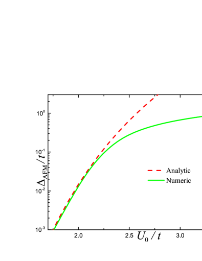
The total gap in the spectrum is given by Eq. (22). It coincides with the AFM order parameter if the bias voltage is zero. The dependence of the gap on the ratio U0/tsubscript𝑈0𝑡U_{0}/t for zero bias is shown in Fig. 2. The analytical expression Eq. (III.2) works well for U02.3tsubscript𝑈02.3𝑡U_{0}\leq 2.3t.

If V00subscript𝑉00V_{0}\neq 0, 
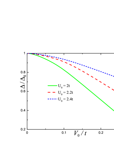
the exciton order parameter becomes non-zero. The full gap ΔΔ\Delta, however, decreases when V0subscript𝑉0V_{0} increases. The dependence of the full gap ΔΔ\Delta on V0subscript𝑉0V_{0} calculated for three different values of U0subscript𝑈0U_{0} is shown in Fig. 3. As it follows from this figure, the gap suppression is stronger for smaller U0subscript𝑈0U_{0}.

We consider here only the case of zero temperature. In this case the full gap never reaches zero for realistic values of the applied voltage. At finite temperatures, however, it can be fully suppressed by the bias voltage. This makes it possible to observe a voltage-driven metal-insulator transition.

Refer to caption
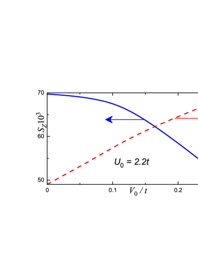
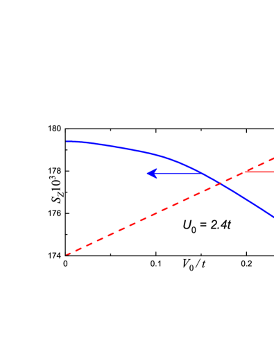
Figure 2: (Color online) AFM order parameter ΔAFMsubscriptΔAFM\Delta_{\textrm{AFM}} versus the on-site interaction U0subscript𝑈0U_{0}, for zero bias V0=0subscript𝑉00V_{0}=0.
Refer to caption
Figure 3: (Color online) Full gap ΔΔ\Delta versus the applied bias V0subscript𝑉0V_{0}, for different values of the on-site Coulomb repulsion U0subscript𝑈0U_{0}. The value Δ0subscriptΔ0\Delta_{0} is equal to the full gap if V0=0subscript𝑉00V_{0}=0, that is, it is the AFM gap ΔAFMsubscriptΔAFM\Delta_{\textrm{AFM}} for zero bias.
Refer to caption
Refer to caption
Refer to caption
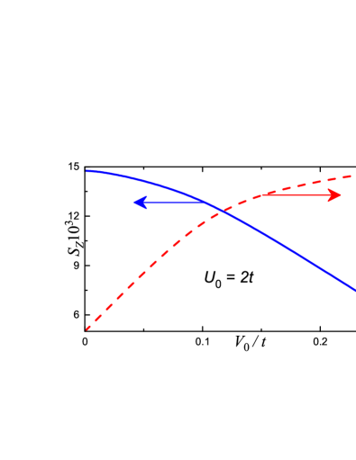
Figure 4: (Color online) The dependence of the AFM magnetization Szsubscript𝑆𝑧S_{z} and of the exciton magnetization ϕitalic-ϕ\phi on the bias voltage V0subscript𝑉0V_{0} for three different values of the on-site interaction U0subscript𝑈0U_{0}. The blue continuous curves are the AFM magnetization Szsubscript𝑆𝑧S_{z}, while the red dashed curves are for the exciton magnetization ϕitalic-ϕ\phi. For all panels we use the value U12=U0/4subscript𝑈12subscript𝑈04U_{12}=U_{0}/4.

Let us analyze now the dependencies of the AFM and exciton order parameters on the applied voltage. For the typical values of the system parameters U02.2tsimilar-to-or-equalssubscript𝑈02.2𝑡U_{0}\simeq 2.2t, U12/U01/4similar-to-or-equalssubscript𝑈12subscript𝑈014U_{12}/U_{0}\simeq 1/4, and V0/t01similar-to-or-equalssubscript𝑉0subscript𝑡01V_{0}/t_{0}\simeq 1, the values of the order parameters are ΔAFM0.17similar-to-or-equalssubscriptΔAFM0.17\Delta_{\textrm{AFM}}\simeq 0.17 eV and Δexc8similar-to-or-equalssubscriptΔexc8\Delta_{\textrm{exc}}\simeq 8 meV. We can rewrite the expressions for the order parameters in terms of magnetizations

Szsubscript𝑆𝑧\displaystyle S_{z} =\displaystyle= 2ΔAFMU0=nn1𝒜nn1𝒜,2subscriptΔAFMsubscript𝑈0delimited-⟨⟩subscript𝑛𝑛1𝒜absentdelimited-⟨⟩subscript𝑛𝑛1𝒜absent\displaystyle\frac{2\Delta_{\textrm{AFM}}}{U_{0}}=\langle n_{n1{\cal A}\uparrow}\rangle-\langle n_{n1{\cal A}\downarrow}\rangle, (35)
ϕitalic-ϕ\displaystyle\phi =\displaystyle= 2ΔexcU12=dn1𝒜dn2𝒜dn1𝒜dn2𝒜.2subscriptΔexcsubscript𝑈12delimited-⟨⟩subscriptsuperscript𝑑𝑛1𝒜absentsubscriptsuperscript𝑑absent𝑛2𝒜absentdelimited-⟨⟩subscriptsuperscript𝑑𝑛1𝒜absentsubscriptsuperscript𝑑absent𝑛2𝒜absent\displaystyle\frac{2\Delta_{\textrm{exc}}}{U_{12}}=\langle d^{\dagger}_{n1{\cal A}\uparrow}d^{\phantom{\dagger}}_{n2{\cal A}\uparrow}\rangle-\langle d^{\dagger}_{n1{\cal A}\downarrow}d^{\phantom{\dagger}}_{n2{\cal A}\downarrow}\rangle.

In these equations, the AFM magnetization Szsubscript𝑆𝑧S_{z} is equal to the magnetization per site of the sublattice 𝒜𝒜{\cal A} in layer 1. For the G-type AFM order, the magnetizations of electrons located at neighboring sites have opposite signs.

The exciton magnetization ϕitalic-ϕ\phi can be viewed as the spin located on the link connecting the sites A1𝐴1A1 and A2𝐴2A2 (for definitions of A1𝐴1A1 and A2𝐴2A2, see Fig. 1). The spin on the link connecting carbon atoms B1𝐵1B1 and B2𝐵2B2 has oppposite sign. The dependence of Szsubscript𝑆𝑧S_{z} on the applied bias voltage calculated for three different values of the on-site interaction constant U0subscript𝑈0U_{0} is shown in Fig. 4 by the solid lines. This magnetization is suppressed by the bias voltage. The suppression is stronger for smaller U0subscript𝑈0U_{0}. When U0>2.4tsubscript𝑈02.4𝑡U_{0}>2.4t, the magnetization Szsubscript𝑆𝑧S_{z} only slightly depends on V0subscript𝑉0V_{0}. The exciton magnetization ϕitalic-ϕ\phi is shown in Fig. 4 by dashed lines. It increases almost linearly with V0subscript𝑉0V_{0}. Nevertheless, ϕitalic-ϕ\phi is much smaller than Szsubscript𝑆𝑧S_{z}, even for relatively large V0subscript𝑉0V_{0}.

III.4 Exciton order parameter

In the limit of small interactions U12,U0tmuch-less-thansubscript𝑈12subscript𝑈0𝑡U_{12},U_{0}\ll t, the second equation in (III.2) simplifies and reduces to

Δexc=ΔAFMV2t0U12U0.subscriptΔexcsubscriptΔAFM𝑉2subscript𝑡0subscript𝑈12subscript𝑈0\displaystyle\Delta_{\textrm{exc}}=\Delta_{\textrm{AFM}}\frac{V}{2t_{0}}\frac{U_{12}}{U_{0}}. (36)

In this limit the value of the exciton order parameter depends linearly on the inter-plane repulsion U12subscript𝑈12U_{12}. References Joglekar, ; Min, ; Perali, ; Rossi, ; Sokolik, ; Efetov, considered a system with two graphene layers separated by an insulating layer. The dielectric barrier between the layers completely suppresses the interlayer tunneling and destroys the AFM order. In this case, the value of the exciton order parameter depends exponentially on the Coulomb interaction between the layers. Under such conditions, according to Ref. Efetov, , the exciton gap becomes exponentially small around 1 mK. In this case, a small amount of disorder makes exciton condensation impossible Das_Sarma . In our case, the exciton order parameter depends almost linearly on U12subscript𝑈12U_{12}. Thus, the exciton order parameter can exist in our system even if the inter-plane interaction is rather small.

Can we detect this order parameter? In principle, the exciton condensation can be observed experimentally by measuring the Coulomb drag How_to ; Das_sarma_drag ; Coulomb_drag . The experimental observation of Coulomb drag in bilayer graphene systems with a dielectric barrier between the layers has been reported Gorbachev_drag . The execution and interpretation of similar experiment on bilayer graphene without the insulating layer might be a much more complicated issue.

All the above results were obtained at zero temperature. The detailed study of the temperature dependence of the AFM order parameter at zero bias voltage was performed in Ref. Last_paper, . Since the graphene bilayer is a two dimensional system, it does not have a distinct magnetic phase transition. However, we can define a crossover temperature Tsuperscript𝑇T^{*} between the short-range antiferromagnetic and paramagnetic states. The calculations done in Ref. Last_paper, show that T0.5ΔAFMsuperscript𝑇0.5subscriptΔAFMT^{*}\approx 0.5\Delta_{\text{AFM}}. For realistic values of the applied voltage the exciton order parameter is much smaller than the AFM order parameter. Consequently, ΔexcTmuch-less-thansubscriptΔexcsuperscript𝑇\Delta_{\text{exc}}\ll T^{*}. However the exciton order parameter is tied with the AFM order parameter, and we expect that they both have the same crossover temperature about, Tsuperscript𝑇T^{*} at V0=0subscript𝑉00V_{0}=0. Since the AFM order parameter can be high enough, the exciton order parameter can survive at relatively high temperatures.

IV Conclusions

In this paper we have studied theoretically the electronic properties of biased AA stacked bilayer graphene. The model Hamiltonian was analyzed in the mean-field approximation. At zero bias, the ground state of the system is antiferromagntic. We found that the applied transverse voltage stabilizes the exciton order parameter coexisting with the AFM order. This new order parameter couples the electrons and holes in different graphene layers. The AFM phase with the coexisting exciton order parameter is the most stable phase if the bias voltage is non-zero. The electronic gap is partially suppressed by the bias voltage leading to a tunable metal-insulator transition. The value of the exciton order parameter can be about several tens of meV. Despite this small value, the exciton order parameter can survive at relatively high temperatures due to its coexistence with the AFM phase.

Acknowledgments

This work was supported in part by RFBR (Grants Nos. 14-02-00276, 14-02-00058, 12-02-00339), the RIKEN iTHES Project, MURI Center for Dynamic Magneto-Optics, and a Grant-in-Aid for Scientific research (S).

References

  • (1)
  • Castro Neto et al. (2009) A.H. Castro Neto, F. Guinea, N.M.R. Peres, K.S. Novoselov, and A. K. Geim, Rev. Mod. Phys. 81, 109 (2009).
  • Abergel et al. (2010) D.S.L. Abergel, V. Apalkov, J. Berashevich, K. Ziegler, and T. Chakraborty, Adv. Phys. 59, 261 (2010).
  • Rozhkov et al. (2011) A.V. Rozhkov, G. Giavaras, Y.P. Bliokh, V. Freilikher, and F. Nori, Physics Reports 503, 77 (2011).
  • McCann and Fal’ko (2006) E. McCann and V. I. Fal’ko, Phys. Rev. Lett. 96, 086805 (2006); E.V. Castro, N.M.R. Peres, T. Stauber, and N.A.P. Silva, ibid., 100, 186803 (2008); R. Nandkishore and L. Levitov, ibid. 104, 156803 (2010a); Phys. Rev. B 82, 115124 (2010b); F. Zhang, H. Min, M. Polini, and A.H. MacDonald, ibid. 81, 041402(R) (2010a).
  • (6) Y. Lemonik, I.L. Aleiner, C. Toke, and V.I. Fal’ko, ibid., 82, 201408(R) (2010); O. Vafek and K. Yang, ibid., 81, 041401 (2010); J. Nilsson, A.H. Castro Neto, N.M.R. Peres, and F. Guinea, ibid., 73, 214418 (2006)
  • (7) S. Novoselov, E. McCann, S.V. Morozov, V.I. Fal’ko, M.I. Katsnelson, U. Zeitler, D. Jiang, F. Schedin, and A.K. Geim, Nat. Phys. 2, 177 (2006); S. Latil and L. Henrard, Phys. Rev. Lett. 97, 036803 (2006); B. Partoens and F.M. Peeters, Phys. Rev. B74, 075404 (2006); H. Min, B. Sahu, S.K. Banerjee, and A.H. MacDonald, Phys. Rev. B75, 155115 (2007).
  • Feldman et al. (2009) B.E. Feldman, J. Martin, and A. Yacoby, Nat. Phys. 5, 889 (2009).
  • Mayorov et al. (2011) A.S. Mayorov D.C. Elias, M. Mucha-Kruczynski, R.V. Gorbachev, T. Tudorovskiy, A. Zhukov, S.V. Morozov, M.I. Katsnelson, V.I. Fal’ko, A.K. Geim, K.S. Novoselov, Science 333, 860 (2011).
  • (10) E. V. Castro, K. S. Novoselov, S. V. Morozov, N. M. R. Peres, J. M. B. Lopes dos Santos, Johan Nilsson, F. Guinea, A. K. Geim, and A. H. Castro Neto, Phys. Rev. Lett. 99, 216802, (2007).
  • (11) Y. Zhang, T-T. Tang, C. Girit, Z. Hao, M. C. Martin, A. Zettl, M. F. Crommie, Y. R. Shen and F. Wang, Nature 459, pp 820-823 (2009).
  • (12) H. Fukidome, M. Kotsugi, K. Nagashio, R. Sato, T. Ohkochi, T. Itoh, A. Toriumi, M. Suemitsu, T. Kinoshita, Sci. Rep. 4, (2014).
  • (13) C.-H. Park and S. G. Louie, Nano Lett. 10, pp 426 431, (2010).
  • de Andres et al. (2008) P.L. de Andres, R. Ramírez, and J.A. Vergés, Phys. Rev. B 77, 045403 (2008).
  • Prada et al. (2011) E. Prada, P. San-Jose, L. Brey, and H. Fertig, Solid State Commun. 151, 1075 (2011).
  • Chiu et al. (2010) C.W. Chiu, S.H. Lee, S.C. Chen, F.L. Shyu, and M.F. Lin, New J. Phys. 12, 083060 (2010).
  • Ho et al. (2010) Y.-H. Ho, J.-Y. Wu, R.-B. Chen, Y.-H. Chiu, and M.-F. Lin, Appl. Phys. Lett. 97, 101905 (2010).
  • Liu et al. (2009) Z. Liu, K. Suenaga, P. J. F. Harris, and S. Iijima, Phys. Rev. Lett. 102, 015501 (2009).
  • Borysiuk et al. (2011) J. Borysiuk, J. Soltys, and J. Piechota, J. of Appl. Phys. 109, 093523 (2011).
  • (20) J.-K. Lee, S.-Ch. Lee, J.-P. Ahn, S.-Ch. Kim, J.I.B. Wilson, and P. John, J. Chem. Phys. 129, 234709 (2008).
  • (21) A.L. Rakhmanov, A.V. Rozhkov, A.O. Sboychakov, and F. Nori, Phys. Rev. Lett. 109, 206801 (2012).
  • (22) A.O. Sboychakov, A.L. Rakhmanov, A.V. Rozhkov, and F. Nori, Phys. Rev. B87, 121401(R) (2013).
  • (23) A.O. Sboychakov, A.V. Rozhkov, A.L. Rakhmanov, and F. Nori, Phys. Rev. B 88, 045409 (2013).
  • (24) J. P. Eisenstein, A. H. MacDonald, Nature, 432, pp 691-694 (2004)
  • (25) D. Nandi, A. D. K. Finck, J. P. Eisenstein, L. N. Pfeiffer, K. W. West, Nature, 488, pp 481-484, (2012)
  • (26) C.-H. Zhang and Y. N. Joglekar, Phys. Rev. B 77, 233405 (2008).
  • (27) H. Min, R. Bistritzer, J.-J. Su, and A. H. MacDonald, Phys. Rev. B 78, 121401 (2008).
  • (28) A. Perali, D. Neilson, and A. R. Hamilton, Phys. Rev. Lett. 110, 146803 (2013).
  • (29) J. Zhang and E. Rossi, Phys. Rev. Lett. 111, 086804 (2013).
  • (30) Y. E. Lozovik, S. L. Ogarkov, and A. A. Sokolik, Phys. Rev. B 86, 045429 (2012),
  • (31) S. Banerjee, L. Register, E. Tutuc, D. Reddy, and A. Mac- Donald, Electron Device Letters, IEEE 30, 158 (2009).
  • Charlier et al. (1992) J.-C. Charlier, J.-P. Michenaud, and X. Gonze, Phys. Rev. B 46, 4531 (1992).
  • (33) H.J. Xiang, E.J. Kan, Su-Huai Wei, X.G. Gong, and M.-H. Whangbo, Phys. Rev. B 82, 165425 (2010); B.S. Pujari, S. Gusarov, M. Brett, and A. Kovalenko, Phys. Rev. B 84, 041402(R) (2011); L. Openov, A. Podlivaev, Semiconductors, 46, 199 (2012); L. Openov, A. Podlivaev, Physica E 44, 1894 (2012); L. Openov, A. Podlivaev, Technical Physics 57, 1603 (2012).
  • (34) T.O. Wehling, E. Şaşıoğlu, C. Friedrich, A.I. Lichtenstein, M.I. Katsnelson, and S. Blügel, Phys. Rev. Lett. 106, 236805 (2011); A. Du, Y.H. Ng, N.J. Bell, Z. Zhu, R. Amal, and S.C. Smith, J. Phys. Chem. Lett. 2, 894 (2011).
  • (35) M. Schuler, M. Rosner, T.O. Wehling, A.I. Lichtenstein, and M.I. Katsnelson, Phys. Rev. Lett. 111, 036601 (2013).
  • (36) R.P. Feynman, Phys. Rev. 56, 340 (1939).
  • (37) M.Yu. Kharitonov and K.B. Efetov, Semicond. Sci. Technol., 25 (2010).
  • (38) D.S.L. Abergel, M. Rodriguez-Vega, E. Rossi, and S. Das Sarma, Phys. Rev. B 88, 235402 (2013).
  • (39) E.H. Hwang, R. Sensarma, and S. Das Sarma, Phys. Rev. B84, 245441 (2011).
  • (40) J. Su and A.H. MacDonald, Nature Physics 4, 799 - 802 (2008).
  • (41) R.V. Gorbachev, A.K. Geim, M.I. Katsnelson, K.S. Novoselov, T. Tudorovskiy, I.V. Grigorieva, A.H. MacDonald, S.V. Morozov, K. Watanabe, T. Taniguchi, and L.A. Ponomarenko, Nature Physics 8, 896 901 (2012).

Appendix A Analytic solution

Here we derive the analytical formulas for the AFM and exciton order parameters. We introduce dimensionless quantities δAFM=ΔAFM/tsubscript𝛿AFMsubscriptΔAFM𝑡\delta_{\textrm{AFM}}=\Delta_{\textrm{AFM}}/t and δexc=Δexc/tsubscript𝛿excsubscriptΔexc𝑡\delta_{\textrm{exc}}=\Delta_{\textrm{exc}}/t. It is convenient to rewrite the exciton order parameter in the following form

δexc=δAFMV2t0b,subscript𝛿excsubscript𝛿AFM𝑉2subscript𝑡0𝑏\displaystyle\delta_{\textrm{exc}}=\delta_{\textrm{AFM}}\frac{V}{2t_{0}}b\,, (37)

where b𝑏b is the new variable. Using this substitution we can rewrite Eqs. (25) and (26) in the form

4tU04𝑡subscript𝑈0\displaystyle\frac{4t}{U_{0}} =\displaystyle= 03𝑑ζρ0(ζ)[1δAFM2+(ζζ0)2+1ζ+ζ0]limit-fromsuperscriptsubscript03differential-d𝜁subscript𝜌0𝜁delimited-[]1superscriptsubscript𝛿𝐴𝐹𝑀2superscript𝜁subscript𝜁021𝜁subscript𝜁0\displaystyle\!\!\!\int\limits_{0}^{3}\!\!d\zeta\,\rho_{0}(\zeta)\!\!\left[\frac{1}{\sqrt{\delta_{AFM}^{2}+(\zeta-\zeta_{0})^{2}}}+\frac{1}{\zeta+\zeta_{0}}\right]-
03𝑑ζρ0(ζ)V2(1b)4t2ζ0ζ[1δAFM2+(ζζ0)21ζ+ζ0],superscriptsubscript03differential-d𝜁subscript𝜌0𝜁superscript𝑉21𝑏4superscript𝑡2subscript𝜁0𝜁delimited-[]1superscriptsubscript𝛿𝐴𝐹𝑀2superscript𝜁subscript𝜁021𝜁subscript𝜁0\displaystyle\!\!\!\!\!\!\!\!\!\!\int\limits_{0}^{3}\!\!d\zeta\,\rho_{0}(\zeta)\frac{V^{2}(1-b)}{4t^{2}\zeta_{0}\zeta}\!\!\left[\frac{1}{\sqrt{\delta_{AFM}^{2}+(\zeta-\zeta_{0})^{2}}}-\frac{1}{\zeta+\zeta_{0}}\right],
4tU124𝑡subscript𝑈12\displaystyle\frac{4t}{U_{12}}\!\! =\displaystyle= 03𝑑ζρ0(ζ)[1δAFM2+(ζζ0)2+1ζ+ζ0]+limit-fromsuperscriptsubscript03differential-d𝜁subscript𝜌0𝜁delimited-[]1superscriptsubscript𝛿𝐴𝐹𝑀2superscript𝜁subscript𝜁021𝜁subscript𝜁0\displaystyle\!\!\!\int\limits_{0}^{3}\!\!d\zeta\,\rho_{0}(\zeta)\!\!\left[\frac{1}{\sqrt{\delta_{AFM}^{2}+(\zeta-\zeta_{0})^{2}}}+\frac{1}{\zeta+\zeta_{0}}\right]+
03𝑑ζρ0(ζ)t02(1b)t2ζ0ζb[1δAFM2+(ζζ0)21ζ+ζ0],superscriptsubscript03differential-d𝜁subscript𝜌0𝜁superscriptsubscript𝑡021𝑏superscript𝑡2subscript𝜁0𝜁𝑏delimited-[]1superscriptsubscript𝛿𝐴𝐹𝑀2superscript𝜁subscript𝜁021𝜁subscript𝜁0\displaystyle\!\!\!\!\!\!\!\!\!\!\int\limits_{0}^{3}\!\!d\zeta\,\rho_{0}(\zeta)\frac{t_{0}^{2}(1-b)}{t^{2}\zeta_{0}\zeta b}\!\!\left[\frac{1}{\sqrt{\delta_{AFM}^{2}+(\zeta-\zeta_{0})^{2}}}-\frac{1}{\zeta+\zeta_{0}}\right],

Taking the integration in Eq. (A) we obtain in the limit δAFM1much-less-thansubscript𝛿AFM1\delta_{\textrm{AFM}}\ll 1

4tU04𝑡subscript𝑈0\displaystyle\frac{4t}{U_{0}} =\displaystyle= ρ0(ζ0)(1V2(1b)4t2ζ02)ln(4ζ0(3ζ0)δAFM2)+limit-fromsubscript𝜌0subscript𝜁01superscript𝑉21𝑏4superscript𝑡2superscriptsubscript𝜁024subscript𝜁03subscript𝜁0superscriptsubscript𝛿AFM2\displaystyle\rho_{0}(\zeta_{0})\left(1-\frac{V^{2}(1-b)}{4t^{2}\zeta_{0}^{2}}\right)\ln\left(\frac{4\zeta_{0}(3-\zeta_{0})}{\delta_{\textrm{AFM}}^{2}}\right)+ (40)
η1(ζ0)+V2(1b)4t2ζ0η2(ζ0)+O(δAFM2),subscript𝜂1subscript𝜁0superscript𝑉21𝑏4superscript𝑡2subscript𝜁0subscript𝜂2subscript𝜁0𝑂superscriptsubscript𝛿AFM2\displaystyle\eta_{1}(\zeta_{0})+\frac{V^{2}(1-b)}{4t^{2}\zeta_{0}}\eta_{2}(\zeta_{0})+O(\delta_{\textrm{AFM}}^{2})\,,

where

η1(ζ0)subscript𝜂1subscript𝜁0\displaystyle\eta_{1}(\zeta_{0})\! =\displaystyle= 03𝑑ζ[ρ0(ζ)ζ+ζ0+ρ0(ζ)ρ0(ζ0)|ζζ0|],superscriptsubscript03differential-d𝜁delimited-[]subscript𝜌0𝜁𝜁subscript𝜁0subscript𝜌0𝜁subscript𝜌0subscript𝜁0𝜁subscript𝜁0\displaystyle\!\int\limits_{0}^{3}\!\!d\zeta\left[\frac{\rho_{0}(\zeta)}{\zeta+\zeta_{0}}+\frac{\rho_{0}(\zeta)-\rho_{0}(\zeta_{0})}{\left|\zeta-\zeta_{0}\right|}\right],\;\;\
η2(ζ0)subscript𝜂2subscript𝜁0\displaystyle\eta_{2}(\zeta_{0})\! =\displaystyle= 03dζζ[ρ0(ζ)ζ+ζ0ρ0(ζ)ζ0ρ0(ζ0)ζζ0|ζζ0|].superscriptsubscript03𝑑𝜁𝜁delimited-[]subscript𝜌0𝜁𝜁subscript𝜁0subscript𝜌0𝜁subscript𝜁0subscript𝜌0subscript𝜁0𝜁subscript𝜁0𝜁subscript𝜁0\displaystyle\!\int\limits_{0}^{3}\!\!\frac{d\zeta}{\zeta}\left[\frac{\rho_{0}(\zeta)}{\zeta+\zeta_{0}}-\frac{\rho_{0}(\zeta)\zeta_{0}-\rho_{0}(\zeta_{0})\zeta}{\zeta_{0}\left|\zeta-\zeta_{0}\right|}\right].\;\;\ (41)

Performing the similar integration in Eq. (A) and expressing the logarithmic term using Eq. (40) we obtain in the limit of small b1much-less-than𝑏1b\ll 1 the following equation for b𝑏b

b=4tU0η1(ζ0)η2(ζ0)ζ04tU124tU0t2ζ02t02+V2(η1(ζ0)+η2(ζ0)ζ0)4t02.𝑏4𝑡subscript𝑈0subscript𝜂1subscript𝜁0subscript𝜂2subscript𝜁0subscript𝜁04𝑡subscript𝑈124𝑡subscript𝑈0superscript𝑡2superscriptsubscript𝜁02superscriptsubscript𝑡02superscript𝑉2subscript𝜂1subscript𝜁0subscript𝜂2subscript𝜁0subscript𝜁04superscriptsubscript𝑡02b\!=\!\frac{\frac{4t}{U_{0}}-\eta_{1}(\zeta_{0})-\eta_{2}(\zeta_{0})\zeta_{0}}{\frac{4t}{U_{12}}\!-\!\frac{4t}{U_{0}}\frac{t^{2}\zeta_{0}^{2}}{t_{0}^{2}}\!+\!\frac{V^{2}(\eta_{1}(\zeta_{0})\!+\!\eta_{2}(\zeta_{0})\zeta_{0})}{4t_{0}^{2}}}. (42)

For the range of parameters U0subscript𝑈0U_{0} and U12subscript𝑈12U_{12} under study, we have b<0.05𝑏0.05b<0.05, so the assumption b1much-less-than𝑏1b\ll 1 is well satisfied. The expression for ΔexcsubscriptΔexc\Delta_{\textrm{exc}} is written as follows

Δexc=ΔAFMV2t04tU0η1(ζ0)η2(ζ0)ζ04tU124tU0t2ζ02t02+V2(η1(ζ0)+η2(ζ0)ζ0)4t02.subscriptΔexcsubscriptΔAFM𝑉2subscript𝑡04𝑡subscript𝑈0subscript𝜂1subscript𝜁0subscript𝜂2subscript𝜁0subscript𝜁04𝑡subscript𝑈124𝑡subscript𝑈0superscript𝑡2superscriptsubscript𝜁02superscriptsubscript𝑡02superscript𝑉2subscript𝜂1subscript𝜁0subscript𝜂2subscript𝜁0subscript𝜁04superscriptsubscript𝑡02\Delta_{\textrm{exc}}\!=\!\Delta_{\textrm{AFM}}\!\frac{V}{2t_{0}}\frac{\frac{4t}{U_{0}}-\eta_{1}(\zeta_{0})-\eta_{2}(\zeta_{0})\zeta_{0}}{\frac{4t}{U_{12}}\!-\!\frac{4t}{U_{0}}\frac{t^{2}\zeta_{0}^{2}}{t_{0}^{2}}\!+\!\frac{V^{2}(\eta_{1}(\zeta_{0})\!+\!\eta_{2}(\zeta_{0})\zeta_{0})}{4t_{0}^{2}}}\,. (43)

The antiferromagnetic gap is found from Eq. (40), where we can neglect b𝑏b in the first and third terms. As a result, we obtain

ΔAFM=2tζ0(3ζ0)exp(η1(ζ0)+η2(ζ0)V24t2ζ024tU02ρ0(ζ0)t02t2ζ02).subscriptΔAFM2𝑡subscript𝜁03subscript𝜁0subscript𝜂1subscript𝜁0subscript𝜂2subscript𝜁0superscript𝑉24superscript𝑡2superscriptsubscript𝜁024𝑡subscript𝑈02subscript𝜌0subscript𝜁0superscriptsubscript𝑡02superscript𝑡2superscriptsubscript𝜁02\Delta_{\textrm{AFM}}\!=\!2t\!\sqrt{\!\zeta_{0}(\!3\!-\!\zeta_{0}\!)}\!\exp\!\left(\!\frac{\eta_{1}(\zeta_{0})+\frac{\eta_{2}(\zeta_{0})V^{2}}{4t^{2}\zeta_{0}^{2}}-\frac{4t}{U_{0}}}{2\rho_{0}(\zeta_{0})\frac{t_{0}^{2}}{t^{2}\zeta_{0}^{2}}}\!\right)\!. (44)