Transient lateral photovoltaic effect in patterned metal-oxide-semiconductor films
Abstract
The time dependent transient lateral photovoltaic effect has been studied with time resolution and with chopping frequencies in the kHz range, in lithographically patterned 21 nm thick, 5, 10 and 20 wide and 1500 long Co lines grown over naturally passivated p-type Si (100). We have observed a nearly linear dependence of the transitorial response with the laser spot position. A transitorial response with a sign change in the laser-off stage has been corroborated by numerical simulations. A qualitative explanation suggests a modification of the drift-diffusion model by including the influence of a local inductance. Our findings indicate that the microstructuring of position sensitive detectors could improve their space-time resolution.
pacs:
78.56.-a; 72.40.+w;73.50.PzWhen photo-carriers are generated locally in a non-uniformly illuminated surface or interface, a photovoltaic response can be measured parallel to the Schottky barrier between two distant lateral contacts. This behavior is known as the lateral photovoltaic effect (LPE) WALLMARK1957 ; Lucovsky1960 ; Boeringer1994 ; Zhao2006 . The LPE originates from the diffusion of carriers out of the illuminated area and it has been widely used to develop high precision position-sensitive detectors (PSD) Yu2010 ; Jin2013 .
During the last decades, the main way of optimizing the sensitivity of LPE based PSDs has been achieved by the use of metal-semiconductor junctions, and quite recently metal-oxide-semiconductor junctions (MOS) with different types of metals (Ti, Co, …) Willens1986 ; Xiao2008 . The particular interest shown in Co/SiO2/Si structures is related to the possibility of developing broadband PSD for the visible, ultraviolet or infrared range Xiao2007 ; Kong2008 ; Qi2010 by adjusting the Co thickness. Previous studies of MOS structures, including Co/SiO2/Si, investigated the LPE by illuminating a relatively large (about ) rectangular samples. A laser beam of a few mW was focused into a 10-50 spot and the open circuit LPE was measured between two contacts which extended along opposite edges Xiao2007 ; Qi2010 ; Yu2010 . In wide devices, the dynamic response is dominated by the barrier capacitance which results in a unipolar (charge-discharge type) response Kronic1999 which diminishes in amplitude when the chopper frequency approaches the kHz range Kabra2008 . Moreover, the steady state LPE value diminishes substantially when the Co thickness approaches 20 nm Xiao2008 . Recent advances in electron beam lithography have permitted the development of MOS structures where the LPE can investigated along patterned, micron wide, metallic line structures. The time dependent photovoltaic response along such structures might be different from the one observed in the wide LPE devices.
Our work investigates the lateral photovoltaic effect in lithographically patterned (21 nm thick, 5, 10 and 20 wide and 1500 long) Co lines. The structures were deposited on a naturally passivated (about 2 nm SiO2) Silicon (100) substrate. More details on preparation and characterization of samples may be found in Brems2007 ; Herranz2009 .
We have studied the transient photovoltaic effect (T-LPE) Dhariwal1976 ; Vieira1997 ; Zhao2006 as a response to turning the laser beam illumination on (steady state, referred to as the ON state) followed by switching the laser off (decaying regime, referred to as the OFF state) as a function of the spot position, pulse frequency and power. We observe peak-like transitorials which present a sign inversion of the T-LPE in the off state followed by a nearly exponential relaxation back to equilibrium. We have corroborated this behavior of the T-LPE response with numerical simulations. We have also qualitatively explained the results with a simple model which takes into account the local inductance of the metallic line structure deposited on top of a Schottky barrier. We observe a substantial increase of the position sensitivity of patterned line structures when their width is reduced, measured by the peak to peak response.
The optical setup depicted in Fig. 1(a) comprises a microscope objective lens (MO) (50x, 0.42 NA, Plan APO, working distance 21 mm) that focuses the laser beam into the sample. The image of the sample is relayed into a CCD camera by using the objective and a beam splitter. A diagram of the LPE device examined in this study is also shown. The potential difference created along the line is measured from three pairs of Cobalt pads which are contacted with gold wires by using indium. The transient LPE has been studied by applying a train of periodic laser beam pulses. TOPTICA-iBeam Smart diode lasers which emit light of 405 or 487 nm of wavelength have been used. The typical response of our device to a laser pulse with is shown in Fig. 1(b), and is discussed in detail below. Both wavelengths are compared in the supplemental material SuppMat .
The T-LPE signal between contacts was amplified in two stages. The first stage is a home-made low noise preamplifier (bandwidth from DC to 1 MHz) with a maximum gain of 47 is followed by a low noise SR750 amplifier with a tunable gain and filter bandwidth. Fig. 1(c) shows that depending on the roll-off frequency of the amplifier filter, the detection of the fast “laser off” transition can be affected. The voltage, amplified up to times, was measured using a NI-PCI 5922 digitizer which works at frequencies up to 2MHz. The square wave used to modulate the laser pulses was supplied by a Keithley K6221 current source. A number of experimental parameters were controlled by computer software, such as the sample motion (via Zaber T-L-A linear actuator), the frequency of the pulses, the power of the laser beam and data acquisition.
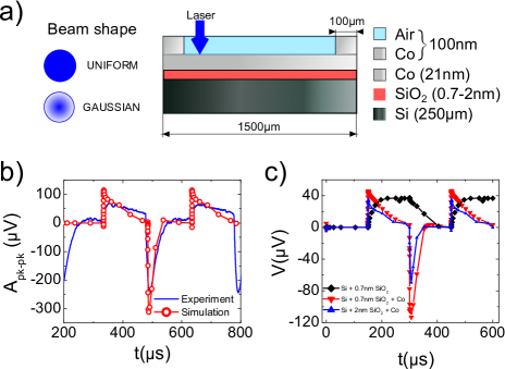
A finite element analysis software ATLAS (by SILVACO) along with the LUMINUS optoelectronic module has been used to simulate the LPE on multilayered structures.
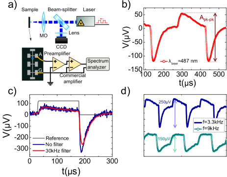
Figure 1(d) presents the T-LPE measured for a 10 wide Co line at different chopping frequencies. One notes that in the ON stage, the T-LPE voltage first increases and then gradually decreases. In the OFF stage the T-LPE voltage shows a fast sign inversion followed by slow, nearly exponential decay down to zero. By using a low-pass filter we obtain a better signal-to-noise ratio, which does not alter the measurement except for the amplitude of the negative peak (see Fig. 1(c)). We found that the optimum chopping frequency for which the T-LPE response is effectively analyzed ranges around a few kHz. As shown in Fig. 1(d), the peak to peak () amplitude somewhat depends on the chopping frequency. This optimum frequency range is restricted from below by the maximum digitizer rate and from above by typical relaxation rate in T-LPE. Most of the experimental results presented below correspond to T-LPE in 10 wide Co line measured with a 3.3 kHz chopping frequency and a focused beam spot size of 2 . Measurements in 20 and 5 wide Co line structures show a qualitatively similar T-LPE response, but with different amplitudes (see below).
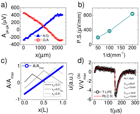
Figure 2(a) presents the amplitude of the T-LPE voltage as a function of the position of the laser spot on top of the Co line, relative to the distance from the reference (grounded) contact. The laser beam power is P=2 mW, which corresponds to the end of the linear and the beginning of the saturated response regime SuppMat . Figure 2(b) shows the estimated position sensitivity (P.S.) in for our 20 , 10 and 5 wide samples, as a function of with the width of the Co line. The sensibility of the samples is estimated from the slope of a linear fit of the amplitude vs. position graphs (see for example Figure 2(a)). More information on the analysis of the amplitude as a function of laser power can be found in the supplemental material SuppMat .
As can be seen in Fig. 2(b), the position sensitivity substantially improves as the samples are made narrower. This suggests that making the PSD narrower and using the peak to peak T-LPE response in such structured sensors could be a simple and effective way to substantially improve their time-space sensitivity. Among the factors which could limit the applicability of microstructuring by optimizing the width are the laser spot dimensions and the characteristics of the material. They could include a possible reduction of the diffusion of photocarriers or the vulnerability of these narrow line structures to ambient conditions (e.g. edge oxidation).
We observe that far from the electrodes that the LPE amplitude has a close to linear dependence on the spot position (Fig. 2(a)), which is one of the most important characteristics of previously studied planar LPE devices WALLMARK1957 ; Lucovsky1960 ; Boeringer1994 ; Zhao2006 . This behavior is independent of the contact configuration with respect to the ground (Fig. 2(a)). Interestingly, however, the T-LPE amplitude and its peak to peak values appear to show finite (above experimental resolution) values when spot is centered exactly between the electrodes. We attribute this offset to a difference in the boundary conditions for the diffusive carriers close the electrodes. The grounded electrode (G) is described as having a small Co contact resistance and the electrode that is connected to the preamplifier (A) which has a much larger input resistance. We have been able to reproduce qualitatively the existence of such an offset by using a one dimensional drift-diffusion model WALLMARK1957 ; Lucovsky1960 which calculates the stationary potential distribution (lines) and potential difference (dots) employing two different (Robin / 3-rd type) boundary conditions (see Figure 2(c) and the supplemental materialSuppMat ).
An earlier model, which describes the dynamic T-LPE response in wide two-dimensional structures WALLMARK1957 ; Lucovsky1960 , is capable only of explaining the charge-discharge dynamic response similar to an RC circuit (local resistance-capacitance). In order to explain the peak-like T-LPE and its sign inversion in the off state we propose introducing an additional term (second time derivative) in the differential equation for the potential distribution . This new term corresponds to the local inductance due to presence of the metallic wire:
| (1) |
where , , the relation between terms and describes the carrier diffusion along the device and F corresponds to the electron-hole separation function. The time dependent solution of equation (1), at a fixed , corresponds to a driven harmonic oscillator, or RLC circuit:
| (2) |
We have found an excellent agreement with our experimental results, as shown in Figure 2(d), for the case when equation 1 describes an underdamped oscillator very close to the overdamped regimeSuppMat . Using the resistance of the 10 Co line, we obtain an estimate of the capacitance and inductance of the strip from the fit (see Fig. 2(d)). The resistance of the 5 sample is twice that of the 10 strip, and using as capacitance half of what was obtained for the 10 sample, we obtain values of inductance which are 60 % higherSuppMat .
Our numerical simulations, with adjusted parameters and a wavelength have reproduced qualitatively the main experimental findings as can be seen in Figure 3(a,b). The main simulation parameters which resulted in the best fit to the experiment are shown below and discussed in the supplemental material SuppMat . We attribute some differences between the experiment and simulation to the capacitance of a real sample as well as the influence of the pre-amplifier, absent in the simulations. In order to check if the observed effects are specific to MOS structures, we have also simulated the T-LPE under the same conditions by decreasing the SiO2 layer thickness (or removing it altogether), shown in Fig. 3(c). When we remove both SiO2 and Co layers and leave only the laterally contacted Si surface, the transient LPE response of the pure Si substrate shows an exponential increase (decrease) when the laser is switched ON (OFF) (Fig. 3(c)).
In conclusion, we have studied the transient lateral photoeffect in patterned metal-oxide/semiconductor structures with widths of several microns. The dependence of the T-LPE with the spot position is almost linear and the time dependent response shows a sign inversion after the laser is switched off. The dynamic response has been explained by the influence of a local inductance, in addition to what was previously considered for wider LPE devices: a local capacitance (generation/recombination process) and resistance. Our findings could stimulate the development of micron-wide position sensitive detectors with improved time-space resolution needed in microrobotics Ivan2012 and other fields where a precise control of the trajectory is required.
The authors acknowledge A. Levanuyk for his interest and fruitful
discussions, L. Martin for her simulations on the initial stages of the work
and Ch. van Haesendock for preparing the samples. This work has been supported by the
Spanish MINECO (MAT2012-32743) and Comunidad de Madrid (P2009/MAT-1726) grants.
* Corresponding author: farkhad.aliev@uam.es
References
- (1) J. T. Wallmark, Proceedings of the Institute of Radio Engineers 45, 474 (1957).
- (2) G. Lucovsky, J. Appl. Phys. 31, 1088 (1960).
- (3) D.W. Boeringer, R. Tsu, Appl. Phys. Lett., 65, 2332 (1994).
- (4) K. Zhao, K.J. Jin, H. Lu, Y. Huang, Q. Zhou, M. He, Z. Chen, Y. Zhou, G. Yang, Appl. Phys. Lett. 88, 141914 (2006).
- (5) C. Yu, H. Wang, Sensors, 10, 10156 ( 2010).
- (6) W. Jin, S. Zhang, H. Ni, W. Xiang, J. Xi, X. Feng, and K. Zhao, International Journal of Photoenergy, 2013, 352738 (2013).
- (7) R.H, Willens, Appl. Phys. Lett., 49, 663 (1986).
- (8) S. Q. Xiao, H. Wang, Z. C. Zhao, Y. Z. Gu, Y. X. Xia and Z. H. Wang, Opt. Express 17, 3798 (2008).
- (9) S. Q. Xiao, H. Wang, Z. C. Zhao, Y. Z. Gu, Y. X. Xia and Z. H. Wang, Optics Express 16, 3799 (2008).
- (10) L. Z. Kong, H. Wang, S. Q. Xiao, J. J. Lu, Y. X. Xia, G.J. Hu, N. Dai and Z.H.Wang, J. Phys. D: Appl. Phys. 41 052003 (2008).
- (11) C. Q. Yu, H. Wang, Appl. Phys. Lett. 96, 171102 (2010).
- (12) L. Kronik, Y. Shapira, Surface Science Reports, 37, 1 (1999).
- (13) D. Kabra, J. Verma, N. S. Vidhyadhiraja, and K. S. Narayan, IEEE SENSORS JOURNAL 8, 1663 (2008).
- (14) S. Brems, K. Temst, C. Van Haesendonck, Phys. Rev. Lett. 99, 067201 (2007).
- (15) D. Herranz, R. Guerrero, R. Villar, F. G. Aliev, A. C. Swaving, R. A. Duine, C. van Haesendonck, I. Vavra, Phys. Rev. B79, 134423 (2009).
- (16) S. R. Dhariwal, L.S. Kothari, and S C Jains, J. Phys. D: Appl. Phys., 9, (1976).
- (17) M. Vieira, Appl. Phys. Lett. 70, 220 (1997).
- (18) See the supplementary material at HTML for details.
- (19) H.B. Lu, K.J. Jin, Y.H. Huang, Meng He, Kun Zhao, Bo-Lin Cheng, Appl. Phys. Lett., 86, 241915 (2005)
- (20) D.M.Kim, J.W. Lee, T. Dosluoglu, R. Solanki, F.Qian, Semicond. Sci. Technol. 9, 1276 (1994).
- (21) I. A. Ivan, M. Ardeleanu, G. J. Laurent, Sensors, 12, 16771 (2012).