Modeling Near-Surface Bound Electron States in Three-Dimensional Topological Insulator: Analytical and Numerical Approaches
Abstract
We apply both analytical and ab-initio methods to explore heterostructures composed of a three-dimensional topological insulator (3D TI) and an ultrathin normal insulator (NI) overlayer as a proof ground for the principles of the topological phase engineering. Using the continual model of a semi-infinite 3D TI we study the surface potential (SP) effect caused by an attached ultrathin layer of 3D NI on the formation of topological bound states at the interface. The results reveal that spatial profile and spectrum of these near-surface states strongly depend on both the sign and strength of the SP. Using ab-initio band structure calculations to take materials specificity into account, we investigate the NI/TI heterostructures formed by a single tetradymite-type quintuple or septuple layer block and the 3D TI substrate. The analytical continuum theory results relate the near-surface state evolution with the SP variation and are in good qualitative agreement with those obtained from density-functional theory (DFT) calculations. We predict also the appearance of the quasi-topological bound state on the 3D NI surface caused by a local band gap inversion induced by an overlayer.
pacs:
73.20.-r, 75.70.CnI Introduction
It is generally recognized that there is one-to-one correspondence between the presence of nontrivial topological invariants characterizing the bulk electron states of a crystal and the appearance of specific electron modes localized at the crystal boundary Fu2 ; Moore1 ; Essin ; Hasan ; Qi ; Okuda ; Ando2013 . This statement, which is known as the bulk-boundary correspondence theorem, reflects profound interrelation between the interior and exterior electron states of the truncated crystal. While the formulated assertion is based on general arguments of the topological concept for solids, in real materials and/or heterostructures, the effect of the peculiar bulk properties on the surface may be quite intricate. This problem has been widely discussed in the context of an existence of topological bound states on the surface of a three-dimensional topological insulator (3D TI) or at the interface between 3D TI and topologically trivial material in various hybrid structuresHasan ; Qi ; Okuda ; Ando2013 . Angle-resolved photoemission spectra have given evidence for the Dirac-like dispersion and the momentum-dependent spin texture of the 3D TI surface states in a family of Bi- and Sb-based narrow-gap semiconductors with strong spin-orbit coupling (SOC) Hasan ; Qi ; Okuda ; Eremeev1 , which leads to the inverted band structure characterized by nontrivial topological invariants.
Although the topologically protected surface states are often considered as the most important and even decisive property of 3D TIs, in practice, the specific manifestations of the boundary-related electron properties in semiconductor materials with an inverted energy gap go far beyond the bulk-boundary correspondence paradigm. In other words, being formally correct, the topological arguments tell us too little about characteristics of the topologically protected surface/interface states (e.g., the details of the dispersion, actual length scale, spin texture) or what other in-gap electron states might form at the real boundary of a 3D TI material. While a rapid progress has been made in investigations of the vacuum-terminated TI surfaces Hasan ; Qi ; Okuda ; Eremeev1 , it is still challenging to control the properties of the Dirac states under the surface modification in complex situations when a 3D TI is brought into the contact with some substances. Recent experiments on 3D TIs have demonstrated that these states are notably sensitive to external perturbations, such as chemical doping of the surface via deposition of both magnetic and nonmagnetic elements Wray ; Scholz ; Valla , oxidation of air-exposed samples Kong , change of the surface termination Eremeev1 ; Miao , capping layers and interfaces with other materials Jenkins ; Berntsen , applying an external gate voltage Chen ; Checkelsky , etc.
Perturbation of a bulk crystal potential exists naturally in truncated crystals and, in particular, 3D TIs, and creates a surface potential (SP) affecting electron properties of a crystal near/at the surface. In Refs. Bianchi ; Bahramy it was argued that a bulk-truncated surface of bismuth-chalcogenides can develop complex electronic structure in which the Dirac states coexist with the conventional states of the two-dimensional electron gas (2DEG) in the quantum well appearing near the 3D TI surface due to the band-bending effect. The ab initio calculations Menshch2011 ; Eremeev2 have shown that an expansion of the van-der-Waals (vdW) spacing in layered 3D TIs caused by intercalation of deposited atoms leads to a simultaneous emergence of 2DEG bands localized in the subsurface region. Moreover, the expansion of the vdW spacing also leads to a relocation of the Dirac topological states to the lower quintuple layers Eremeev2 . Wang et al have studied the effects of surface modification on the topological surface state in Bi2Se3 using first-principles calculations and shown that Bi-capping and Se-removing can move the Dirac point upwards and slow flatten the topological surface bands Wang . The short-range chemical forces related to dangling-bonds on the surface of a thallium-based ternary chalcogenides TIs (TlBiTe2, TlBiSe2, TlSbTe2, and TlSbSe2) produce strong surface states Eremeev3 which can be removed by thallium adatoms Kuroda2013 . In Ref. LZhao it was suggested that the Dirac point of the helical surface states can be significantly shifted by applying uniaxial strain.
Many exciting physical properties of the Dirac helical quasiparticles (in particular, spin-dependent transport) are predicted to provide good opportunities for different spintronic applications Garate ; Yu ; Fujita ; Pesin . To fully embody these promising ideas in devices, one requires multiple interfaces with the topologically trivial materials rather than a single pristine surface of TI. Using density functional theory to design superlattice structures based on Bi2Se3, it was shown that an interface state with an ideal Dirac cone is caused by alternating the layers of 3D TI and 3D normal insulator (NI) Song . The authors of Ref. Zhang have studied theoretically the Sb2Se3/Bi2Se3 heterostructures, the constituents of which possess the Bloch functions of the same symmetry. They found that the probability maximum of the Dirac state largely moves from the topologically nontrivial Bi2Se3 into the region of the topologically trivial Sb2Se3. On the other hand, ARPES experiments YZhao provide the direct evidence that the surface state of top surface of the heterostructure containing single quintuple layer (QL) of Bi2Se3 on 19QLs of Bi2Te3 is similar to the surface state of Bi2Se3. Moreover, the transport measurements YZhao show that the studied heterostructure behaves more like Bi2Se3 even though there is only 1QL Bi2Se3 layer grown on 19QLs Bi2Te3. In Refs. Wu ; Li it was established that, as a result of depositing a 3D NI overlayer (conventional semiconductor ZnM, M=S, Se, and Te) onto the 3D TI substrate (Bi2Se3 or Bi2Te3), the topological states can float to the top of the NI film, or stay put at the NI/TI interface, or are pushed down deeper into 3D TI. Recently Berntsen and colleagues have directly observed the Dirac states at the Bi2Se3/Si(111) buried interface Berntsen . Another photoemission study in Ref. Nakayama revealed an existence of the interface topological states in the layered bulk crystal (PbSe)5(Bi2Se3)3m, which forms a natural multilayer heterostructure composed of TI and NI. The evidence of a large shift of the Dirac point towards the conduction band edge relative to the case of the 3D TI/vacuum interface, due to the In2Se3 Jenkins or Sb2Se2Te Tania capping layer on the epitaxial Bi2Se3 thin film, was reported demonstrating a possibility of controlling the Dirac cone in 3D TI-based systems.
Thus, the experimental and theoretical data exhibit that the real 3D TI surface and 3D TI/NI interface possess very rich and diverse physics, in particular, they can hold both topological and non-topological (ordinary) in-gap states. It is well known that the non-topological bound states can be created or deleted or altered, depending on the both the sign and strength of SP, when 3D NI is exposed to ambient conditions or put into the contact with other materials. On the contrary, in 3D TI, the topological order itself is robust against such the influences so that it can be completely destroyed only under the drastic perturbation Chena ; Eremeev4 . Nevertheless, the parameters of the topological states can undergo remarkable changes with even moderate external perturbations. Combination of the robustness of the topological states at the TI/NI interfaces with the tunability of their parameters to the external influence favours the design of the 3D TI/NI layered systems possessing suitable band structure, charge distribution and spin texture. The efficient design of the 3D TI/NI systems can be realized by combining analytic and numerical methods.
In the present work, we consider a special type of the 3D TI/NI heterostructures of particular interest, which contain an ultrathin film of nonmagnetic NI (overlayer) artificially deposited on a relatively thick film of 3D TI (substrate). Due to a specific relation between electron affinities and band gap widths of the substrate and overlayer materials, significant modifications of the spectrum and wave function of the Dirac states are expected as compared to the pristine 3D TI surface (i.e. the 3D TI/vacuum interface), thus making it possible to obtain the 3D TI-based heterostructure with tailor-made electron properties. One assumes that the substrate film thickness is large enough to avoid sizable hybridization of the bound states appearing at the opposite boundaries of the film. At the same time, the minimal thickness of the overlayer is formally limited by the condition of an electron motion quantization in the 3D NI material. Under these restrictions, to describe analytically the electron bound states near the surface of the truncated 3D TI covered by the 3D NI overlayer, the continual approach involving the method of effective surface potential (SP) was offered in Ref. Men . In what follows, we will use the term ’near-surface state’ (see also Ref. Men ) for identification of the in-gap electron state localized in the subsurface region and driven by the overlayer-induced SP. Just recently, in Ref. Tania , several preliminary results concerning the near-surface states in the 3D TI/NI heterostructures with realistic material parameters has been obtained within the numerical simulations based on density functional theory (DFT). Below , we employ the two complementary approaches – analytical and numerical – in order to elucidate thoroughly the important question how a 3D NI overlayer affects the electron properties of 3D TI/NI heterostructures.
In the framework of the analytical approach, it is instructive to re-formulate this question in terms of the boundary conditions at the TI/NI interface for the wave function of the system. It is clear that, in systems composed of two topologically distinguishable materials, the characteristics of the near-surface state depend crucially on the choice of the boundary conditions, which still remains highly disputable subject (for example, see Refs. Shan ; Medhi ; Michetti ). The wave function at the ideal atomic interface between a pair of similar materials (e.g., 3D TI Bi2Se3 and 3D NI Sb2Te3 have the same crystal symmetry) satisfies the Ben-Daniel&Duke boundary conditions BenDaniel . While matching the wave function at the contact of two dissimilar materials (e.g., such as Si and Bi2Se3) is complicated within the formalism because the envelope function (EF) on each side of the interface are defined using distinct orbital basis (see Ref. Tokatly and reference therein). However, such complication proved to be circumvented for the particular models describing different types of contacts within the effective interface potential concept Men2010 ; Menshov ; Men2013 .
Below, in the framework of the continual approach involving the SP scheme, we formulate general boundary conditions for the long-range envelope function of the truncated 3D TI and truncated 3D NI and find the solution for the bound near-surface states. We restrict ourselves to the situation when solely the orbital degree of freedom of electrons is manipulated by external influence at the surface. We succeed in general qualitative understanding of the dependence of the energy spectrum and spatial profile of the near-surface states on an effective SP. Furthermore, in order to elucidate the fine details of the near-surface state transformation induced by the overlayer, we employ the material-specific DFT calculations for the 3D TI/NI heterostructures. For the conceptual reasons, within an effective SP scheme, we also discuss the near-surface states in the fictitious heterostructures of other types, in which a substrate of a 3D NI close to the quantum transition into a 3D TI phase is covered with an overlayer of either NI or TI material.
The paper is organized as follows. In Sec. 2, we discuss the effective SP concept, propose the model for a truncated TI covered with an overlayer, and introduce the main ingredients and assumptions of the problem within the continual approach. In Sec. 3, for the case of a spin-independent surface perturbation caused by an overlayer, we thoroughly investigate how the corresponding SP modifies the electron energy spectrum and the EF spatial profile of the Dirac-like near-surface state. In Sec. 4, we analyze main features of the near-surface state in a situation when a 3D NI substrate close to transition into a topological phase is covered with a ultrathin overlayer of either a NI material or a TI one. To corroborate the SP formalism results , in In Sec. 5, we apply the DFT calculations and analyze the band structure and wave-function of the bound near-surface states for a set of heterostructures formed by a single tetradymite-type quintuple (QL) or septuple (SL) layer blocks and 3D TI substrates. Finally, the main conclusions are presented in Sec. 6.
II Surface potential concept and model hamiltonian
Apart from the aforementioned simulations of the properties of 3D TIs based on the first principle calculations, various continual models have been discussed to describe relativistic fermions at the TI boundary Zhang ; Liu ; Shan . There are theoretical studies of the TI properties, which are routinely based on the simple phenomenological 2D Hamiltonian for helical fermions with the linear Dirac-cone-like energy-momentum dispersion under an external influence Fu : , where is the unit vector normal to the surface, is the Fermi velocity, is the vector composed of the Pauli matrices. It is generally thought that a controllable external field, , can be directly applied to the 3D TI surface to manage its electron states. For instance, a spin-independent term could simulate the energy shift of the Dirac-cone point due to an electrostatic potential caused by a nonmagnetic overlayer. In turn, a spin-dependent term could generate a gapped spin-polarized surface state through an exchange field proportional to the magnetization applied along the normal to the surface of 3D TI which is in contact with a ferromagnetic insulator Garate ; Tserkovnyak ; Yokoyama . In this manner, to take into account a perturbation arising from the external influence, the additional term is simply included in the 2D Hamiltonian , without a serious analysis of the microscopic origin of both and . The vast majority of theoretical works restricts to such the description and they predict many curious effects which can be realized in the 3D TI-based structures. However, the 2D Hamiltonian can formally be derived from a relevant 3D Hamiltonian only under the free surface stipulation in the spirit of Refs. Zhang ; Shan . In the framework of the consistent scheme, the bound near-surface states for the half-infinite 3D TI are composed of the eigen-states of the corresponding bulk 3D TI Hamiltonian. Meanwhile, note that so far nobody has written down the full set of the orthogonal wave-functions (including the bound and extended along -direction states) for the Hamiltonian of 3D TI in the half-infinite geometry even under the free boundary conditions on the surface. Strictly speaking, the bound states alone do not form the full basis set suited for correct description of the field effect on 3D TI. The external surface perturbation excites electron density in the bulk 3D TI region of a nanoscopic scale adjacent to the surface. Both the bound and extended electron modes give rise to the response of 3D TI to this perturbation. Upon placing the 3D NI on 3D TI, besides the topological bound state, the so-called ordinary bound state Menshov can arise near the interface due to the hybridization between the NI and TI atomic orbitals through the interface. Hence the near surface electron density perturbation of the 3D TI has very complicated spatial, orbital and spin configuration. The phenomenological 2D Hamiltonian hardly could serve as a starting point for the correct analysis of the configuration-dependent response of the 3D TI. So, to correctly take into account the effect of an external perturbation on the surface/interface electron states in the 3D TI, one has to directly include the field into the ”true” 3D Hamiltonian of the system.
A basic idea to go beyond the scope of the 2D model is the use of the well-known method Bir . To characterize the band electron states of a bulk semiconductor, ( is a wave vector, is a band index), in the region of the Brillouin zone around the point of band extrema , the method is reputed to be accurate enough. Under a perturbation smooth on the atomic scale, this method makes it possible to predict evolution of the electron state wave function in terms of a product of a slowly varying envelope function (EF) and the Bloch function of the unperturbed crystal at the point : , is the lattice periodic function. The EF concept may also be applied to the description of localized and resonant interface states in the semiconductor junctions of different types. However, a relevant choice of the boundary conditions for the function remains an unsettled question in this concept, in particular for the TI based structures. The authors of Refs. Zhang ; Shan impose the so-called ’open’ boundary conditions fixing all EF components to zero at the crystal surface. This restriction formally simulates the effect of vanishing of the quasiparticle wave function on the infinitely high SP barrier. Nevertheless, it should be pointed out that the zero constraint is not unique, and other options for boundary conditions have been advocated in the literature. For instance, in Ref. Medhi the problem is formulated in terms of an energy functional whose minimization yields the so-called ’natural’ boundary conditions, intermixing the magnitudes and derivatives of different EF components. Both mentioned types of the EF boundary conditions are extremely idealized and cannot adequately take into consideration a sensitivity of the 3D TI electron states to the surface modifications.
In this work we propose a formalism to directly incorporate the surface perturbation effect into the 3D TI Hamiltonian. We derive the appropriate EF boundary conditions through the construction of the effective semi-phenomenological SP localized at the 3D TI surface. The orbital and spin structure of the SP mimics induced fields resulting from a surface perturbation. As shown below, the structure and strength of the SP determine both the spatial and spectral features of the topological states.
The low energy and long wavelength bulk electron states of the prototypical TI, narrow-gap semiconductor of Bi2Se3-type, are described by the four bands Hamiltonian with strong SOC proposed in Refs. Zhang ; Liu . Without a loss of generality, we make use of the simple version of this Hamiltonian in the form:
| (1) |
where , is the wave vector, , and () denote the Pauli matrices in the spin and orbital space, respectively. The Hamiltonian is written in the basis of the four states at the point of the Brillouin zone with . The superscripts denote the even and odd parity states and the arrows indicate the spin projection onto the quantization axis. The Hamiltonian (1) captures the remarkable feature of the band structure: under the condition , the inverted order of the energy terms and around , which correctly characterizes the topological nature of the system due to strong SOC. The Hamiltonian (1) is particle-hole symmetric and isotropic, which helps us to simplify calculations.
We consider a semi-infinite 3D TI material, such as Bi2Se3, occupying the region . The material boundary located at is perfectly flat and displays translational symmetry in the plane. The potential at the surface of a real 3D TI material is different from the bulk crystal potential, irrespective of whether the surface is kept in ultra-high vacuum or, for example, coated with an overlayer or interfaced with another material. To demonstrate the effect of the surface modification on the topological states within a conceptually simple scheme, we introduce the interaction of electrons with an external perturbation confined at the surface, implementing the effective SP into the EF calculation. Thus we write the full electron energy of the truncated 3D TI in the following form:
| (2) |
Here the operator determined in Eq. (1) acts in the the spinor function space , represented in the basis , the superscript denotes the transpose operation. The EF components (the subscript numbers the spinor components) are presumed to be smooth and continuous functions in the half-space , while the spatial symmetry and periodicity of the system are broken due to existence of the TI surface. It is evident that the approach cannot provide a correct description of the wave-function behavior near the surface, where large momenta are highly important. To overcome this drawback we introduce the effective SP , which affects the electron states of TI at the surface. The potential is nonzero in a small region (of the order of a lattice parameter) around the geometrical boundary , where the validity of the scheme is questionable. An introduction of the phenomenological SP in Eq. (2) enables us to correctly match the low-energy and long-range electronic states inside the truncated TI with evanescent vacuum states through the boundary conditions for EF . As long as the EF spatial variation of the sought state, [, ], is sufficiently slow in the direction normal to the surface, one can adopt a local approximation for the SP. Namely one writes , where the symbol at the argument of the delta-function signifies that the sheet-like SP is placed inside the TI half-space but at infinitesimally small distance from the boundary .
As a matter of course, an electron wave function has to be continuous at a crystal boundary. Nevertheless, in the system under consideration, since the Bloch factors of the wave function inside and outside TI do not coincide (in particular, they have distinct space symmetries), the long-range EF can formally undergo a finite break (jump) across the boundary from to within the utilized method (we refer the reader to the detailed discussion in Ref. Medhi ). In the current work, we do not care how the wave-function behaves in the half-space but next we make use of a functional
| (3) |
where the energy plays a role of the Lagrange multiplier, is an unit matrix, . The functional (3) is determined in the class of the smooth and continuous EFs in the TI half-space and includes the effective surface potential . Since, in a plane geometry, the wave-vector is a good quantum number, we determine the functional for each EF -mode, . Varying functional with respect to yields the Euler equations for the half-space and the boundary conditions at the surface at . The corresponding equations in the compact form are:
| (4) |
| (5) |
In the left side of Eq. (5) the current density operator acts on the EF spinor. Thus the right side associated with the surface perturbation plays a role of the external (with regard to the TI bulk) current source (sink). The equation (5) involves the surface potential parameters, in this sense it has something in common with the equation which was used to calculate the surface states of a crystal with a relativistic band structure in Ref. Volkov . The solution of the boundary task, Eqs. (4) and (5), answers the principal physical question how the perturbation located just at the TI boundary affects the near-surface topological states.
In the half-space , the general solution of Eq. (4) for each EF spinor component obeying the condition can be represented as
| (6) |
where
| (7) |
| (8) |
Here the phase factors forming the spinor depend only on the momentum polar angle, , ; the signs relates to lower and upper spectral branches, respectively. The characteristic momenta are the solutions of the corresponding secular equation; . The boundary conditions, Eq. (5), determine the coefficients and as well as the dispersion relation for the near-surface states inside the bulk band gap, . The parameter is implied to be .
III Near-surface topological bound states
The potential in Eq. (5) is a matrix specifying internal properties of the TI surface and the matrix elements include different components of scattering of the TI states on SP. In principle, choosing the structure of the matrix and the strength of its components allows us to tune spatial and energy characteristics of the topological states. For example, as for the SP diagonal matrix elements, , the values and are proportional to the scattering intensity of particle and hole, respectively, on the spin-independent part of SP, while the quantities and are proportional to the scattering intensity of particle and hole, respectively, on the -component of the exchange part of SP. The off-diagonal matrix elements with result from the spin-orbit interaction at the surface, which, in general different from the SOC in the TI bulk.
In this work we focus on the SP that preserves time reversal symmetry, i.e. , where , . Such the SP structure in the basis results in the following relations between the EF coefficients in Eq. (6): , , , . Moreover, we neglect the dependence of on in Eq. (5).
One can interpret the spin-independent scattering on the surface within the framework of a ’local band bending’ scheme (which is quite reasonable for the contact of two insulators/semiconductors), where the band edge corresponding to the -th spinor component is affected by the external perturbation confined at the surface: . In the situation of TI covered with an overlayer the intuitive idea is that the diagonal components of SP could be heuristically adjusted to the relative offsets between the corresponding energy levels (bands) of the TI substrate and the overlayer. In other words, the energy mimics the local bending of the respective bands.
After some algebra the corresponding secular equation results in the implicit relation between the energy and the in-plane momentum for the bound state at the TI surface:
where in accordance with Eqs. (7) and (8), . Note that Eq. (III) is invariant under the simultaneous permutations: , and .
At the point, Eq. (III) is reduced to the equation that determines the Dirac (node) point position, , as a function of the SP strength :
| (10) | |||||
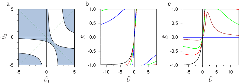
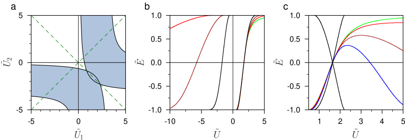
The shaded areas in Fig. 1a denote the realm of the near-surface bound state with on the -plane. The dependence of the node point position on the SP strength, obtained from Eq. (10) for several ratio values , is plotted in Fig. 1b (for ) and Fig. 1c (for ). One can see three different regions in these plots. At weak potential , the Dirac point linearly shifts with respect to the TI bulk bands to either higher or lower binding energies depending on the SP strength sum,
| (11) |
In case the SP strength is large, , the node point energy approaches zero as
| (12) |
On the -plane, there are regions (unshaded areas in Fig. 1a) where the bound state is absent since the node point merges into the conduction or valence bulk band. For example, if , the threshold values of the potential, at which the node point splits off the bulk band continuum, are , so that and .
If the energy is a small deviation from the Dirac linear spectrum, , , the characteristic momenta, Eq. (8), are found as
| (13) |
where is given by Eq. (18). The deviation appears to be small not only when but also when SP is either weak or strong. Using the expression (13) one can obtain the spectrum and estimate the spatial distribution of the near-surface state in these limit situations.
So, for the extremely large potential, , the correction approaches zero, , in turn, the EF coordinate dependence is described by a difference of the exponents, , so that the maximum of the electron density, , does not occur on the surface, where , but rather near the point (where ) that is distant from the surface. Such the EF distribution, together with the linear spectrum, was found under the free boundary conditions Shan . Our approach allows us to capture peculiarities of the surface state in 3D TI induced by the SP. If the SP strength is much greater than the characteristic energy, , within the perturbation theory, one obtains the amendment to the linear dispersion law as
| (14) |
The surface state spectrum acquires a curvature and a shift of the node point, , which are inversely proportional to the potential, however the fermion group velocity near the node point does not change since the amendment (14) does not contain a contribution linear in . In the lowest order in , the relations between the coefficients in Eq. (6) are given by
| (15) |
Thus, the electron density does not vanish on the TI surface, . However, under the SP influence, the EF components can vanish near the surface at , namely, at when , and at when . Besides, as seen from Eq. (13), the SP affects the decay length of the EF nonzero harmonics.
If the SP is formally absent, , one arrives at the solution obtained in Ref. Medhi from using the natural boundary conditions: the surface state shows the linear spectrum and the EF spatial profile in -direction is merely a sum of the two exponents, , i.e., the probability density of the near-surface state is peaked on the boundary and its tail penetrates into the TI bulk with the decay length . In the case of weak SP, , the correction to the dispersion law is given by
| (16) |
The spin-independent SP is seen to entirely shift and warp the energy-momentum dependence. Note, that the corrections (14) and (16) are opposite in the sign. Turning on the SP leads to the different contributions of the quick and slow exponents into EF: .
Let us consider thoroughly the specific case of the staggered alignment of the matrix elements, , when SP does not break the particle-hole symmetry. One can verify in Eq. (III) that in such the case the near-surface state maintains the ideal Dirac spectrum regardless of the size and sign of . While the spectrum is independent of the SP, the envelope function is strongly affected by it. The coordinate dependence of each component of the EF spinor is given by
| (17) |
where
| (18) |
| (19) |
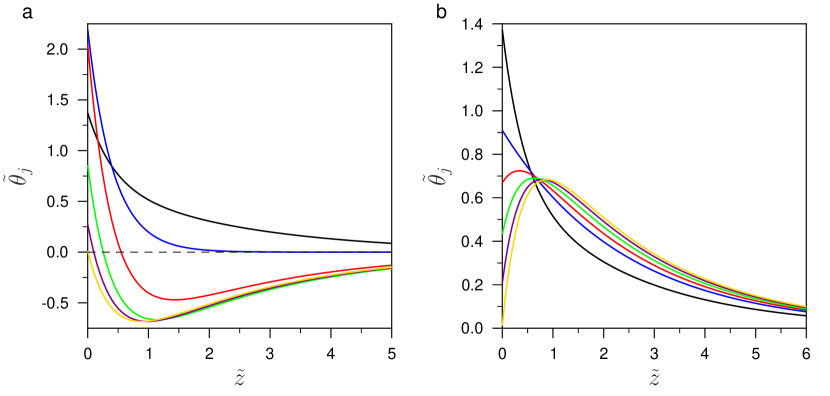
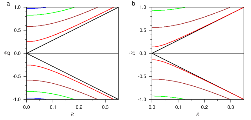
The EF of Eq. (17) is normalized as . The spatial behavior of the EF zeroth harmonic is illustrated in Fig. 2a and Fig. 2b for positive and negative , respectively. With increasing SP strength the EF structure evolves from the sum of the exponents at (black lines) to the difference at (yellow lines). So, one sees a gradual change in the profile of the near-surface state such that its gravity center moves from the surface to the TI interior. It is obvious the behavior of the EF nonzero harmonics Eq. (17) is insignificantly different from what is plotted in Fig. 2; unless the tail at is slightly longer than that at .
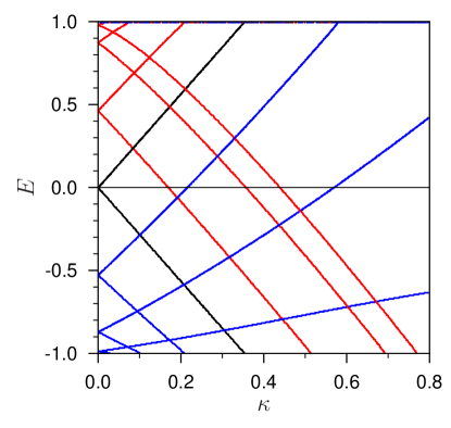
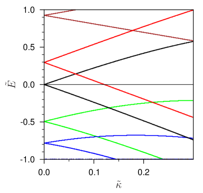
To study the modification of the near-surface states under the finite strength of SP we dwell at length on the situation . As seen in Fig. 3, at a finite strength of , , apart from the aforesaid shift of the node point, the form of the spectral dependence, , alters (in comparison with the limiting cases or ) under the SP influence. The group velocity of the surface topological excitations decreases from the quantity to zero when the SP strength either increases from zero to the threshold value or decreases from infinity to the threshold value . A noticeable deviation from linearity can be seen for the strength . In the limit the dispersion becomes parabolic at small , and in the limit the curve smoothly merges into . The dependence acquires a curvature so that the relatively strong () and relatively weak () potentials provide with the curvature of opposite sing.
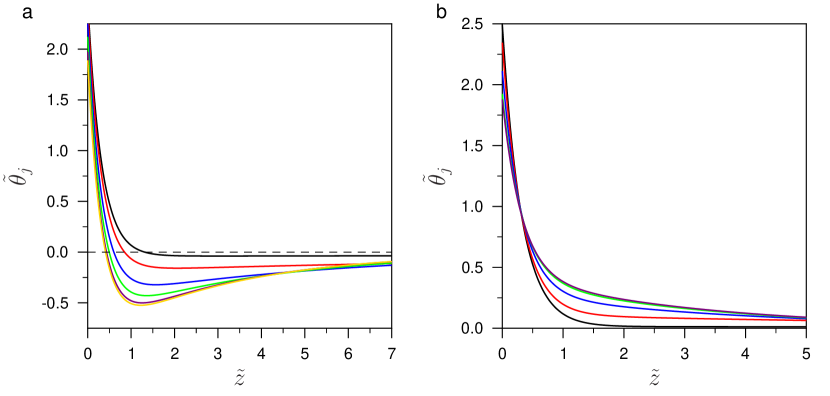
The spatial behavior of the near-surface states for is shown in Fig. 4. When the SP is weak, , the probability density is largely peaked near the surface. The strong SP, , pushes the probability density towards the TI bulk. The EF is exponentially decaying away from the surface. We would like to emphasize that the EF decay lengths, (see Eq. (8)), are strongly influenced by the SP strength. For example, when the strength varies either from to or from to , the momentum increases from to (i.e. the ’long’ exponent of EF (6)) becomes longer) and the momentum decreases from to (i.e. the ’short’ exponent becomes shorter).
IV Quasi-topological bound states near the surface of a normal insulator
Next, we investigate the effect of the surface modification on the near-surface bound states when the bulk is a 3D normal (topologically trivial) insulator. Here we address the fundamental question of whether 3D NI responds to a localized surface perturbation in a way different from 3D TI. In order to describe 3D NI, one uses the same relativistic Hamiltonian (1) in which, however, now there is the normal (non-inverted) alignment of the energy terms of different parity and around is implied, i.e., and . For instance, in the case of the In2Se3 crystal, which shares the same crystal structure with Bi2Se3, the SOC is not strong enough to provide the inversion between two orbitals with opposite parity at the point Zhang . In the limit , when SOC is negligible small, Eq. (1) defines merely the semiconductor with simple (nonrelativistic) two-band spectrum.
It is evident that Eqs. (2)-(5) and the relevant sentences are valid regardless of the sign. Therefore analogously to what has been done in the previous Sections (the details are omitted) one can obtain the characteristics of the bound electron states on the NI surface subjected to the external spin-independent influence. The existence of these states is determined by real solutions of the corresponding secular equation within the bulk gap, , which is given by Eq. (III) at and . Fig. 5a shows the existence realm of the near-surface bound state, i.e., the area on the -plane where . The energy as a function of the SP strength for several ratio values is represented in Fig. 5b (for ) and Fig. 5c (for ). As is seen, except for the quadrant , one may choose the ratio to match the SP which induces the bound electron state on the NI surface.
In what follows, we consider thoroughly only the two particular cases: and . When the SP matrix elements are in staggered rows, , the bound state exists at , which diminishes virtually the 3D NI bulk gap on the surface. Because of the presence of such the SP, the particle-hole symmetry of the system is preserved. The relations between the energy and momentum is given by
| (20) |
where , is the projection of the bulk spectrum onto the surface. In Fig. 6, the spectral dependence is illustrated for several choices of the SP strength . So, the system exhibits a non-linearly dispersing surface state which is specified by the energy gap . The crossing black lines in Fig. 5c show the half gap as a function of . One can see in Fig. 5a and Fig. 5c that the near-surface state stays in the bulk band gap, , when the SP strength is restricted by the interval , where . While, outside this interval, it is buried in the bulk band continuum. In the close vicinity of a band-crossing point , where , the dispersion relation is given by , so that a degeneracy at the band-crossing point is lifted due to gapping . It is convenient to measure the SP strength in the dimensionless units , then , where . In turn, in a small energy window near the bulk band edges, where , the dependence (20) becomes
| (21) |
Note, in the case , Eq. (20) reduces to ; in other words, in the 3D NI under finite value of SOC, a finite strength of SP, , is required to split off the in-gap near-surface state from the 3D bulk continuum.
Such the behavior of the bound state location in energy axis with increasing the SP strength can intuitively be explained in the language of the ’local band bending’ scheme proposed in the previous section. When 3D NI is brought into contact with a thin dielectric overlayer, a relative weak positive SP, , splits off states from both the conduction bulk band and valence one due to a local narrowing of the gap, . At , the local band bending is so steep that the bulk band edges of 3D NI cross over the energy levels of an adjusted overlayer with opposite parity, as it would be if the 3D NI surface was in the contact with a TI overlayer. Further increase of the strength above the critical value pushes the near-surface state into the bulk continuum.
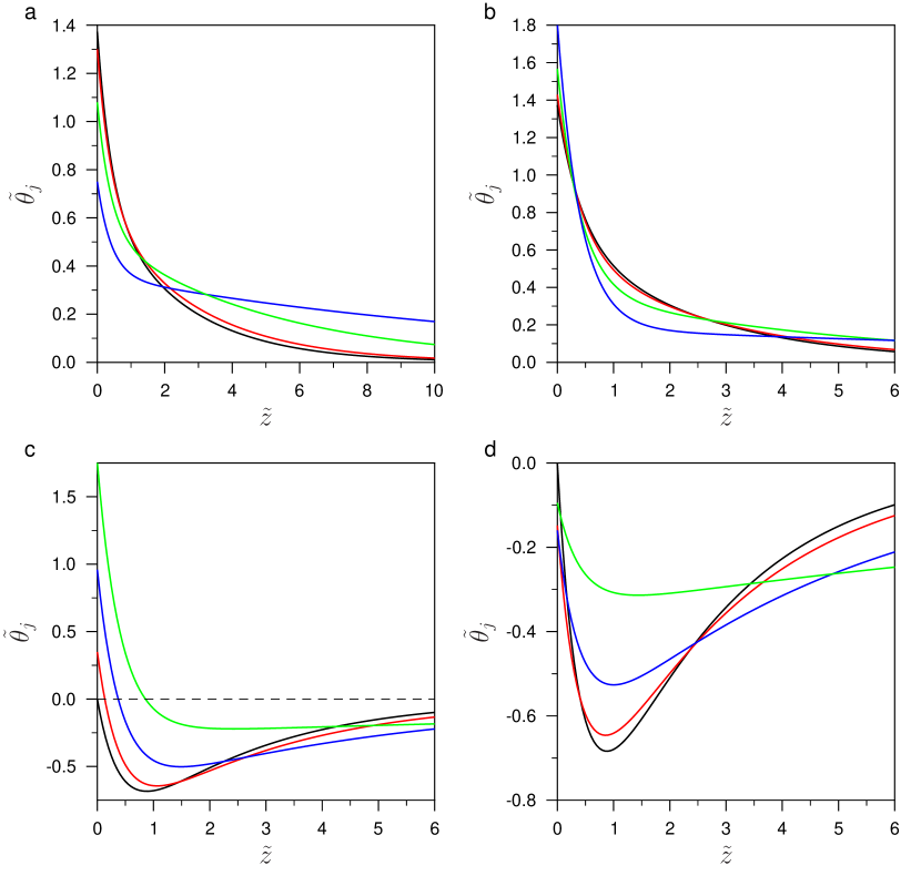
Figure 7 visualizes the effect of the external potential with , on the space profile of the in-gap state of the truncated 3D NI. It is of interest to note that, while crossing the value , the form of the space dependence of the EF zeroth harmonic, , switches over from monotonically decreasing, Fig. 7b, (in the situation of , which mimics the 3D NI/TI-overlayer heterostructure) to nonmonotonically decreasing with minimum at , Fig. 7a, (in the situation of , which mimics the 3D NI/NI-overlayer heterostructure). If , the EF can be approximated as:
| (22) |
| (23) |
When the strength , i.e., , the EF (6) is the superposition of slow exponent with relative small weight and quick one with relative large weight: . This situation is depicted with the black and red curves in Fig. 7.
Let us now draw the attention to the case when the surface perturbation has the spinor structure answering to the surface electrostatic potential. Fig. 8 shows the dispersion law for several values of the SP strength . In the vicinity of the points , where , the relations between the energy and the in-plane momentum (in the leading order in ) is given by
| (24) |
where . Thus, it is clear, given belonging to the interval(s) (where ), the surface state consists of a single Dirac cone. Within the framework of a heuristical ’local band bending’ scheme, the variation of the strength is linked with the relative movement of the energy levels of the 3D NI substrate and the NI overlayer. When the SP strength value exceeds the threshold quantity, , the band structure of this system (which consists of the two materials with a normal gap band alignment) is inverted, i.e., either the substrate conduction band is lower than the overlayer valence band or the substrate valence band is higher than the overlayer conduction band. As a result, if the strength is in the interval , the near-surface state of the NI covered by the normal overlayer can display a linear dispersion dependence of the Dirac-cone form, , where the node point location and propagation velocity are the functions of the strength and band structure parameter . The energy is inside the NI bulk gap, . The quasi-topological bound state is also specified by the space distribution, which is shown in Fig. 9. The corresponding EF decays exponentially away from the surface. When the strength attains the quantity , the near-surface state merges into the bulk continuum states, in turn the decay length becomes large (the black and green curves). At , the probability density is concentrated close to the surface, in other case, it is rather smeared.
V ab initio calculations
The proposed continual approach gives transparent physical explanation for evolution of the near-surface state in both momentum and real spaces with the SP superimposed on the TI or NI boundary. This approach describes fairly well the electron density distribution of the corresponding Dirac-cone-like states on the scale exceeding the lattice spacing through EF(s) as the superposition (see Eq. (6), where the exponents and the coefficients , , are functions of the SP components and the bulk band structure parameters. However, within the SP scheme, we are unable to elucidate the electron density features on the scale on the order of the SP spacing , in particular, capture the fine effect of the the topological state relocation within near-surface layers EremeevPRB2013 ; Wu . Below, in order to provide a closer look at the wave function of the bound near-surface state and to accurately reproduce its band structure over the whole Brillouin zone we present ab initio density functional theory calculation results for some systems representing the topological insulator substrate covered by the insulator ultrathin film.
| NI/TI | (Å)/(Å) | (%) | (eV)/(eV) | (eV)/(eV) |
|---|---|---|---|---|
| GeBi2Te/Bi2Te2S | 4.3225/4.316 | 4.99/5.04 | 0.44/0.27 | |
| Sb2Te2S/Sb2Te2Se | 4.17/4.188 | 4.99/4.62 | 0.47/0.30 | |
| Bi2Te2S/GeBi2Te4 | 4.316/4.3225 | 5.38/4.76 | 0.33/0.08 |
Electronic structure calculations were carried out within the density functional theory using the projector augmented-wave method Blochl1994 as implemented in the VASP code vasp1 ; vasp2 . The exchange-correlation energy was treated using the generalized gradient approximation PBE . The Hamiltonian contained the scalar relativistic corrections and the spin-orbit coupling was taken into account by the second variation method Koelling.jpc1977 . In order to take into account the effect of dispersion interactions we use the van der Waals nonlocal correlation functional within DFT-D2 approach Grimme.jcc2006 .
The thin film NI/TI heterostructures were simulated within a model of repeating slabs separated by a vacuum spacing of 10 Å. The overlayers were symmetrically attached to both sides of the substrate slab to preserve the inversion symmetry.
As the substrates were chosen 3D TIs with tetradymite-like layered structures Bi2Te2S, Sb2Te2Se Menshch2011 ; Eremeev2 composed of quintuple layer (QL) blocks and GeBi2Te4 Menshch2011_2 ; Eremeev1 composed of septuple layer (SL) blocks. The substrates were simulated by 6 QL (5 SL) slabs. As the thin insulating overlayers we used single QL(SL) films of Bi2Te2S, Sb2Te2S, and GeBi2Te4 which have gapped noninverted spectrum. The interface systems under investigation are given in Table 1. As can be seen in Table 1, the lattice mismatch between overlayer and TI substrate in the considered heterostructures doesn’t exceed 0.5 % providing very good epitaxial compatibility. The in-plane lattice parameters of the heterostructures were fixed to the experimental ones of the substrate slab Parameter_1976 ; Grauer_Bi2STe2 ; Karpinsky1998170 . The interlayer distances within the overlayer and the TI block, closest to the interface, were optimized.
Fig. 10a shows spectra of the free-standing GeBi2Te4 overlayer and Bi2Te2S substrate. In the spectrum of Bi2Te2S the topological surface state (TSS) with the Dirac point lying in the valley of the valence bulk states propagates across the bulk energy gap. The spectrum of the free-standing overlayer has the 440 meV gap. The energies of the overlayer states are matched to substrate spectrum in accordance with work functions and given in Tabl. 1. Thus the highest occupied state of the overlayer lies meV above the top of the valence band of substrate. The attaching of the topologically trivial insulating overlayer to TI substrate keeps the gapless topological surface state, however, it leads to strong modification of the spectrum (Fig. 10b): the DP shifts towards the bottom of the conduction band of the substrate so that above the DP it propagates as a resonant state, mixed with bulk-like states of the Bi2Te2S slab. In the real space, the TSS in the heterostructure is almost completely relocated into the overlayer and its probability maximum lies near the GeBi2Te4/Bi2Te2S interface plane (Fig. 10c,d). Such a behavior of the topological state can be explained by the potential change upon the interface formation. In Fig. 10e the change in electrostatic potential of the heterostructure with respect to potentials in free-standing substrate and overlayer is shown. One can see that due to hybridization between orbitals of the overlayer and substrate the potential within the TI substrate is smoothly bent towards the interface plane while the potential within the overlayer undergoes more noticeable changes and as a whole it shifts down by meV with respect to its position in the free-standing overlayer. In spite of the downward shift of the potential the resulting topological state has the Dirac point position higher than in the TSS of the pristine TI surface. The change in the DP position is related to the fact that in the heterostructure the orbitals of GeBi2Te4 contribute more to the TSS than to the orbitals of Bi2Te2S. Thus the modification of the topological state in the considered system is qualitatively similar to the behavior found in the continual model with where for negative beneath a critical value arise solutions with positive shift of the Dirac point (see Fig. 1b).
In the Sb2Te2S/Sb2Te2Se heterostructure (Fig. 11) the TSS dispersion remains almost unchanged with respect to that on the pristine Sb2Te2Se substrate surface being shifted towards the bulk valence band by 40 meV. Along with this, the maximum of charge density of the topological state relocates into the Sb2Te2S QL (Fig. 11c,d) owing to downward shift of the overlayer potential (Fig. 11e) and demonstrates a resonance like behavior due to the DP proximity to the bulk continuum. In the model this scenario is realized at (Fig. 1c) when moderate negative potential at the interface doesn’t leads to substantial change in the energy of the TSS.
A rather distinct type of the TSS modification demonstrate the Bi2Te2S/GeBi2Te4 system (Fig. 12). The work function of the free standing overlayer is eV larger than that of the GeBi2Te4 substrate slab (see Tabl. 1). This means that the gap-edge states of the overlayer are far below the bulk gap of TI substrate (Fig. 12a). In contrast to the previous cases, where at attaching of the overlayer the topological state remains within the bulk gap of the substrate, the TSS in the Bi2Te2S/GeBi2Te4 heterostructure occurs at -0.4 eV, in the local gap of the bulk valence band of GeBi2Te4. This state lies in deep and abrupt potential well of meV depth that causes its strong localization within Bi2Te2S QL. Thus the modification of the TSS in the Bi2Te2S/GeBi2Te4 heterostructure is qualitatively similar to the case (Fig. 1c) in the continual model where large negative value of the potential results in huge shift of the Dirac point down from its position in the initial system.
VI Summary and concluding remarks
In this work, we have shown that the energy spectrum and spatial profile of the near-surface electron states in the 3D TI substrate/NI overlayer type of heterostructures can be controlled by the overlayer induced SP. By choosing an appropriate overlayer it is possible to adjust the Dirac point to the required position in the band gap. The DFT calculations demonstrate clearly how the overlayer-induced shift of the Dirac point from its energy position on the pristine surface is associated with the parameters of the band structure of the 3D TI substrate and the quintuple/septuple overlayer. These results are in good qualitative agreement with the tendency predicted from the analytic continual scheme, in which the overlayer-induced change in the energy spectrum is determined by the SP matrix elements, . Thus the SP matrix elements can be intuitively associated with the relative energy offsets between the relevant band edges of the substrate and overlayer: , , where and are bandgaps and work functions of an overlayer (subscribe 1) and a TI substrate (subscribe 2).
In the framework of the continual approach, we have succeeded in formulating general boundary conditions for the long-range EF and finding the solution for electron bound states at the TI/NI interface. We have obtained analytical expressions for the energy spectrum and EF for different types and values of SP. Our results are strictly consistent with the limiting cases of the zero and infinite surface potentials, which were previously studied in Refs. Shan ; Medhi . The boundary conditions of Eq. (5) involves the SP parameters, in this sense the represented approach has something in common with the one used to calculate the surface states of a crystal with the relativistic band structure Volkov . Note that in Ref. Menshov , the bound states at the interface between 3D TI and NI have been explored on the basis of the functional defined in the entire space. In that work, the explicit expressions for the matrix elements of the interface pseudo-potential, which affects electrons on the TI side of the interface, have been analytically derived.
From the theoretical point of view, one cannot suggest universal recipe to impose the restrictions on the EF behavior at the 3D TI boundary for all types of the heterostructures containing 3D TIs. Note, in particular, that the boundary conditions of Eq. (5) imposed upon the near-surface states are different from those obtained in Ref. Menshov , where, for an interface between 3D TI and a topologically trivial insulator, authors succeeded in a formulation of the EF boundary task, the solution of which provides insight into the electron states at the interface. Although the EF approach may be adapted for the description of the interface states in many semiconductor junctions, by taking into account the general Hermiticity and symmetry requirements Tokatly , this traditional description is not always able to capture the principal features of the topological states in the systems containing narrow-gap semiconductors with inverted band structure and sometimes yields rather dubious results DeBeule . As for the above-stated conception, the appropriate EF boundary conditions are derived within the framework of the formalism of the sheet-like SP. In such the approach, some information (for example, about the effects of electron-electron interaction) is evidently lost that is compensated by a relative calculation simplicity and a transparent physical interpretation. The method, conceptually presented in our work for the study of the truncated 3D TI covered with an atomically thin non-magnetic insulating overlayer, can be straightforwardly extended to solve a wide range of problems related to a behavior of the near-surface topological states under the surface perturbations listed in Introduction.
Indeed, as it is shown in Sec. 4, the area of applicability of the SP method significantly oversteps the formal limits of the 3D TI substrate/NI overlayer systems. We have determined the existence or absence of the Dirac-like near-surface modes in the hypothetical situations when the truncated 3D NI (close to transition into a topological phase) is brought into the contact with the ultrathin overlayer of the 3D NI or TI material. We predict that the near-surface “topological-like” mode can appear in the 3D NI substrate/NI overlayr, i.e., in the system composed only of two topologically trivial materials. This unusual item has something in common with the fact of the appearance of 2D TI state in an InAs/GaSb Type-II semiconductor quantum well (QW) LiuC ; Knez . The unique feature of InAs/GaSb QW is that the conduction band minimum of InAs has lower energy than the valence band maximum of GaSb (due to the large band-offset). Consequently, when the QW thickness is large enough, the first electron subband of InAs layer lies below the first hole subband of GaSb layer, i.e., an inverted band alignment, similar to that in HgTe QWs Hasan ; Qi , happens. The experimental study of low temperature electronic transport have shown strong evidence for the existence of helical edge modes in the hybridization gap of inverted InAs/GaSb QWs Knez .
In view of the aforesaid, one raises the following questions concerning different strategies to create the topological near-surface/interface states and manage their electronic properties: (i) How does a 3D NI overlayer influence a 3D TI? (ii) When one puts an overlayer of one 3D TI on a substrate of another 3D TI, what new property will come into being? (iii) How about a hypothetical 3D TI thin film on the surface states of 3D NI? (iiii) Finally, one could ask how to construct a quasi-topological bound state at the boundary between two topologically trivial insulators? Our work partly answers these questions. The approach proposed above unveils the physics of the near-surface states in the semiconductor heterostructures containing 3D TIs. At the same time, it might be considered as a good guidebook for the qualitative interpretation and forecast of the topological phase behavior tendencies in 3D TIs under surface perturbations. The obtained results should open new opportunities to design various combinations of topological and conventional materials for electronic/spintronic applications.
References
References
- (1) Fu L and Kane C L 2007 Phys. Rev. B 76 045302
- (2) Moore J E and Balents L 2007 Phys. Rev. B 75 121306
- (3) Essin A M and Gurarie V 2011 Phys. Rev. B 84 125132
- (4) Hasan M Z and Kane C L 2010 Rev. Mod. Phys. 82 3045
- (5) Qi X L and Zhang S C 2011 Rev. Mod. Phys. 83 1057
- (6) Okuda T and Kimura A 2013 J. Phys. Soc. Jpn. 82 021002
- (7) Ando Y 2013 J. Phys. Soc. Jpn. 82 102001
- (8) Eremeev S V et al 2012 Nat. Commun. 3 635
- (9) Wray L A et al 2011 Nat. Phys. 7 32
- (10) Scholz M R et al 2012 Phys. Rev. Lett. 108 256810
- (11) Valla T et al 2012 Phys. Rev. Lett. 108 117601
- (12) Kong D et al 2011 ACS Nano 5 4698
- (13) Miao L et al 2013 PNAS 110 2758
- (14) Jenkins G S et al 2013 Phys. Rev. B 87 155126
- (15) Berntsen M H, Götberg O and Tjernberg O 2013 Phys. Rev. B 88 195132
- (16) Chen J et al 2010 Phys. Rev. Lett. 105 176602
- (17) Checkelsky J G et al 2011 Phys. Rev. Lett. 106 196801
- (18) Bianchi M et al 2011 Phys. Rev. Lett. 107 086802
- (19) Bahramy M S et al 2012 Nat. Commun. 3 1159
- (20) Menshchikova T V et al 2011 JETP Lett. 94 106
- (21) Eremeev S V et al 2012 New J. Phys. 14 113030
- (22) Wang X et al 2012 Phys. Lett. A 376 768
- (23) Eremeev S V et al 2011 Phys. Rev. B. 83 205129
- (24) Kuroda K et al 2013 Phys. Rev. B. 88 245308
- (25) Zhao L et al 2012 Appl. Phys. Lett. 100 131602
- (26) Garate I and Franz M 2010 Phys. Rev. Lett. 104 146802
- (27) Yu R et al 2010 Science 329 61
- (28) Fujita T, Jalil M B A and Tan S G 2011 Applied Physics Express 4 094201
- (29) Pesin D and Macdonald A H 2012 Nat. Mater. 11 409
- (30) Song J-H, Jin H and Freeman A J 2010 Phys. Rev. Lett. 105 096403
- (31) Zhang Q et al 2012 ASC NANO 6 2345
- (32) Zhao Y et al 2013 Sci. Rep. 3 3060
- (33) Wu G et al 2013 Sci. Rep. 3 1233
- (34) Li X et al 2013 Chinese Phys. B 22 097306
- (35) Nakayama K et al arXiv:1206.7043v1
- (36) Menshchikova T V et al 2013 Nano Lett. 13 6064
- (37) Eremeev S V, Koroteev Yu M and Chulkov E V 2010 JETP Lett. 91 387
- (38) Chena C et al 2012 PNAS 109 3694
- (39) Men’shov V N, Tugushev V V and Chulkov E V 2013 JETP Lett. 98 603
- (40) Shan W-Y, Lu H-Z and Shen S-Q 2010 New J. Phys. 12 043048
- (41) Medhi A and Shenoy V B 2012 J. Phys. Cond. Mat. 24 355001
- (42) Michetti P et al 2012 Semicond. Sci. Technol. 27 124007
- (43) BenDaniel D J and Duke C B 1966 Phys. Rev. 152 683
- (44) Tokatly I V, Tsibizov A G and Gorbatsevich A A 2002 Phys. Rev. B 65 165328
- (45) Men’shov V N, Tugushev V V and Chulkov E V 2013 JETP Lett. 97 258
- (46) Men’shov V N et al 2010 Phys. Rev. B 81 235212
- (47) Men’shov V N et al 2013 Phys. Rev. B 88 224401
- (48) Liu C X et al 2010 Phys. Rev. B 82 045122
- (49) Fu L 2009 Phys. Rev. Lett. 103 266801
- (50) Tserkovnyak Y and Loss D 2012 Phys. Rev. Lett. 108 187201
- (51) Yokoyama T, Zang J and Nagaosa N 2010 Phys. Rev. B 81 241410
- (52) Bir G L and Pikus G E Symmetry and Strain-Induced Effects in Semiconductors, J. Wiley&Sons, New York/Keter Publishing House, Jerusalem, 1974.
- (53) Volkov V A and Pinsker T N 1981 Sov. Phys. Solid State 23 1022
- (54) Eremeev S V et al 2013 Phys. Rev. B 88 144430
- (55) Blöchl P E 1994 Phys. Rev. B 50 17953
- (56) Kresse G and Furthmüller J 1996 Phys. Rev. B 54 11169
- (57) Kresse G and Joubert D 1999 Phys. Rev. B 59 1758
- (58) Perdew J P, Burke K and Ernzerhof M 1996 Phys. Rev. Lett. 77 3865
- (59) Koelling D D and Harmon B N 1977 J. Phys. C: Sol. St. Phys. 10 3107
- (60) Grimme S 2006 J. Comput. Chem. 27 1787
- (61) Menshchikova T V et al 2011 JETP Lett. 93 15
- (62) Hulliger F 1976 Structural chemistry of layer-type phases (D. Reidel Pub. Co.)
- (63) Grauer D C et al 2009 Materials Research Bulletin 44 1926
- (64) Karpinsky O G et al 1998 J. Alloys and Compounds 265 170
- (65) De Beule C and Partoens B 2013 Phys. Rev. B 87 115113
- (66) Liu C et al 2008 Phys. Rev. Lett. 100 236601
- (67) Knez I, Du R-R and Sullivan G 2011 Phys. Rev. Lett. 107 136603