High-field charge transport on the surface of Bi2Se3
Abstract
We present a theoretical study on the high-field charge transport on the surface of Bi2Se3 and reproduce all the main features of the recent experimental results, i.e., the incomplete current saturation and the finite residual conductance in the high applied field regime [Costache et al., Phys. Rev. Lett. 112, 086601 (2014)]. Due to the hot-electron effect, the conductance decreases and the current shows the tendency of the saturation with the increase of the applied electric field. Moreover, the electric field can excite carriers within the surface bands through interband precession and leads to a higher conductance. As a joint effect of the hot-electron transport and the carrier excitation, the conductance approaches a finite residual value in the high-field regime and the current saturation becomes incomplete. We thus demonstrate that, contrary to the conjecture in the literature, the observed transport phenomena can be understood qualitatively in the framework of surface transport alone. Furthermore, if a constant bulk conductance which is insensitive to the field is introduced, one can obtain a good quantitative agreement between the theoretical results and the experimental data.
pacs:
73.50.Fq, 75.70.Tj, 72.25.RbI Introduction
The three-dimensional topological insulators (TIs) have attracted much attention recently due to the intriggering fundemental physics as well as the possible application in the TI devices.Fu et al. (2007); Zhang et al. (2009); Xia et al. (2009); Hsieh et al. (2009a); Hasan and Kane (2010); Hsieh et al. (2009b); Analytis et al. (2010a); Pan et al. (2011); Chen et al. (2009); Qi and Zhang (2011); Hasan and Moore (2011); Qi et al. (2008); Fiete et al. (2012) TI has a gapped insulating bulk but gappless conducting surface states whose low energy ones can be described as massless Dirac fermions. The discovery of the strong TI materials such as Bi2Se3, which has a bulk gap on the order of 300 meV, are of particular interest since it indicates the feasibility of the room temperature devices. The surface states of the strong TI materials near the Dirac points have been experimentally measured by the spin-angle resolved photoemission spectroscopy.Xia et al. (2009); Pan et al. (2011) However, the signature of the surface states has yet to be separated from the bulk ones in the transport experiments. Due to the relatively small gap, it is commonly believed that the bulk states have strong influence on the charge transport,Culcer (2012); Culcer et al. (2010); Burkov and Hawthorn (2010); Barreto et al. (2013); Skinner et al. (2013); Analytis et al. (2010a); Butch et al. (2010); Analytis et al. (2010b); Eto et al. (2010); *PhysRevB.84.075316; *PhysRevB.84.165311; *PhysRevB.85.155301 even when the Fermi level resides inside the bulk gap.Checkelsky et al. (2011); Ren et al. (2011b, 2012); Costache et al. (2014) However, without a clear understanding of surface transport, it is premature to distinguish the surface transport from the bulk one.
Recently, Costache et al. reported the experimental investigation on the charge transport on the surface of Bi2Se3 under high electric fields.Costache et al. (2014) In the experiment, it is observed that the current increases with the applied voltage in low voltage regime, then shows a tendency of saturation at the intermediate regime. However, the current saturation is not complete. When the voltage further increases to about 50 mV, the current rises again. For conductance, it undergoes slight change in the small voltage regime, then a quick reduction in the intermediate one, and finally saturates in the high applied voltage regime (larger than 50 mV). The current saturation or the conductance reduction is attributed to the inelastic electron-optical-phonon scattering in the surface states. The finite saturated conductance in the high voltage regime, however, is speculated to be the contribution from the bulk ones. It is argued that due to band bending, the energy gap of Bi2Se3 is reduced to be 50 meV from the original 300 meV. Therefore, when the applied voltage is higher than 50 mV, the carriers are excited from surface bands to the bulk band which has finite conductance.Costache et al. (2014) However, this argument is valid only when the transport is nearly ballistic so that the carriers in the surface bands can have enough energy gain to be excited to the bulk bands. However, for the diffusive transport in the experimental setup, the average energy gain is estimated to be less than 4 meV when the applied voltage is 50 mV. This indicates that the excitation of carriers from the surface bands to the bulk one is very unlikely to have significant effect on the transport even if the energy gap is indeed reduced to 50 meV. Therefore, the incomplete saturation and the finite residual conductance are unlikely from the bulk contribution.
Theoretically, the charge and spin transports of the surface state in Bi2Se3 have been investigatedCulcer (2012); Culcer et al. (2010); Burkov and Hawthorn (2010) with most of the studies focusing on the linear transport regime. Zhang and Wu have carried out the study on the hot-electron transport under strong electric field of the surface states in Bi2Se3 by solving the kinetic spin Bloch equations (KSBEs).Zhang and Wu (2013) It is shown that the mobility, and hence the conductance, decreases with increasing applied electric field due to the hot-electron effect. Moreover, it is further shown that the electric field can excite carriers on the surface from the valance to the conduction bands through the interband precession. The excited carriers also contribute to the charge transport, thus lead to an enhanced conductance. Combining these two results, it is possible to understand the qualitative dependence of the current and the conductance on the applied voltage within the framework of the surface transport alone. In this paper, we show that the main features of the experimental results, i.e., the incomplete current saturation and the finite residual conductance, can indeed be captured by the surface transport alone, even though the bulk does have non-neglectable contribution to the total conductance.
This paper is organized as follows: In Sec. II, we set up the model and present the KSBEs. In Sec. III, we show that the main features of the experimental results, such as the incomplete saturation of current and the finite residual conductance at high applied field, can be captured by the surface transport alone. Moreover, we show that one can obtain a good agreement between the experimental results and theoretical calculation by introducing a constant bulk conductance that does not change with the applied voltage. We summarize in Sec. IV
II Model and KSBEs
The Hamiltonian for the electrons on the (001) Bi2Se3 surface grown along the -direction is composed of the free part and the interacting part . The free part describes the low energy surface states around the point and can be written in form of the RashbaBychkov and Rashba (1984) spin-orbit couplingZhang et al. (2009); Liu et al. (2010); Fu (2009)
| (1) |
in which, is set to be 1, is the Fermi velocity which is chosen to be m/s,Culcer et al. (2010) is the annihilation (creation) operator of the electron with the in-plane momentum and spin and are the Pauli matrices for spin. In the collinear spin space spanned by the eigenstates of ( and ), the surface states can be expressed by the two helix spin states , with being the polar angle of the momentum . The and branches, with linear dispersion , correspond to the conduction and valance bands of the surface states, respectively. The interacting part describes the electron-impurity scattering, electron-phonon coupling and electron-electron Coulomb interaction. It can be written as
| (2) |
Here with , and standing for the elementary charge, permittivity, and the dielectric constant of Bi2Se3, respectively. .Richter and Becker (1977); Butch et al. (2010); Zhang and Wu (2013) , where is the position of -th impurity and is the impurity density. , with [] being the annihilation (creation) operators of the phonon with branch , momentum and energy . For the electron-phonon coupling, we include contributions from the surface optical phonon, longitudinal and transverse acoustic phonons.Giraud and Egger (2011); *PhysRevB.85.035441 The matrix elements for the electron-surface optical phonon coupling read
| (3) |
where is the ion mass, is the primitive cell area [meV], eV nm, eV nm2 and meV is the optical phonon energy.Zhang et al. (2009); Zhu et al. (2011) For the longitudinal and transverse acoustic phonon, the matrix elements of the electron-phonon coupling read
| (4) |
| (5) |
respectively.Giraud and Egger (2011); Giraud et al. (2012) In the above equations, , m/s is the longitudinal (transverse) sound velocity,Shoemake et al. (1969); Richter and Becker (1977) kg/m3 is the mass densityWiese and Muldawer (1960); Fu and Kane (2007) and eV.Giraud et al. (2012)
By using the nonequilibrium Green function method,Haug and Jauho (1996) we construct the KSBEs for spatially uniform system as followsWu et al. (2010); Cheng and Wu (2006); Zhang and Wu (2013)
| (6) |
Here is the density matrix for electrons with momentum in the helix spin space. The diagonal elements of , , represent the electron distribution functions in the conduction and valance bands, respectively, while the off-diagonal terms stand for the interband coherence. The KSBEs include the coherent term (the second term in the left-hand-side of the equation), the acceleration of the electron under the electric field (the third term), the interband precession induced by the field (the fourth term) as well as the scattering term (the fifth term). The electric-field-induced interband precession originates from the spin mixing in the conduction and valance bands. Similar effect also exists in the graphene where the pseudospins are mixed.Balev et al. (2009) This term is usually ignored in the previous studies on low field transport.Balev et al. (2009) However, it is shown that the electric-field-induced interband precession has profound influence on the transport properties under high electric field as it leads to a strong excitation of the carriers from the surface valance to the conduction bands.Zhang and Wu (2013) The expressions for the scattering term can be found in Ref. [Zhang and Wu, 2013], which includes the contribution from electron-electron Coulomb interaction, electron-impurity scattering and electron-phonon coupling.
By numerically solving the KSBEs for spatially uniform system, one obtains the charge current density for the applied electric field . We apply our results to a sample with length nm and width nm, the same length and width as those of the sample D2 in Ref. [Costache et al., 2014], in order to obtain the quantities such as the applied voltage and the conductance with the current . Here the prefactor 2 is from the fact that each sample contains two surfaces.
III Numerical Results
In Fig. 1(a), we plot the current as a function of the applied voltage at 4.2 K for the surface states with electron density cm-2 and impurity density cm-2. One can see that our theoretical results capture all the main experimental results qualitatively. Namely, the current increases linearly with the increase of the voltage when the voltage is small; Then the current shows a tendency of saturation at intermediate voltage but increases again when the voltage rises higher than mV. This incomplete saturation can also be seen in the voltage dependence of the conductance , also shown in Fig. 1(a). One finds from the figure that, the conductance decreases as the voltage increases then saturates to a finite constant at higher voltage.
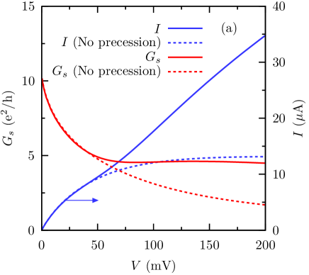
The decrease of the conductance is a result of the hot-electron effect at high electric field.Weng et al. (2004); Zhang and Wu (2013) Due to the driving of the electric field, the temperature of the electrons raises well above the lattice one when the field is high enough. As a result, the electron-phonon scattering is profoundly enhanced, consequently the mobility decreases. Therefore, the conductance decreases with the increase of the voltage. When the field is strong enough, the mobility under electric field is roughly inversely proportional to the electric field . Here is the linear mobility and is a constant that weakly decreases when carrier concentration rises.Zhang and Wu (2013) One can therefore estimate that the current should saturates to at high voltage. This current saturation can be crudely captured by the so called steady-state population model with instantaneous phonon emission.Barreiro et al. (2009); Yao et al. (2000)
If the saturation is complete as predicted by the steady-state population model, the current should remain constant and the conductance should approach zero under high voltage. However, our computation shows that at higher applied electric field, the current saturation is not complete. When the voltage further increases the current again rises linearly with the voltage, and the corresponding conductance saturates to a finite value instead of zero. This incomplete current saturation and the finite residual conductance in the high-field regime is due to the excitation of carriers from the surface valence band to the surface conduction one via the interband precession (the fourth term in KSBEs), first proposed by Zhang and Wu.Zhang and Wu (2013) In the low field regime, the excitation is proportional to . For sample with a high background carrier density, the number of the excited carriers is too small to have an observable effect on transport properties. In the intermediate regime where the mobility is reduced due to the hot-electron effect but the carrier excitation is not yet strong enough, the current shows tendency of saturation as the mobility reduces. At higher field regime, when more carriers are excited, the current increases again with the increases of the field. Under strong field, the excited carrier density is proportional to the electric field , and the total number of the carriers becomes
| (7) |
with being a constant. Combining with the fact that the mobility is inversely proportional to in this regime, one finds that the conductance
| (8) |
It is therefore understood that under strong applied electric field/voltage when the number of the excited carriers exceeds the background one, the conductance becomes a finite constant
| (9) |
The saturated field is determined by the equation , i.e., when the number of the excited carriers becomes the same as the background one. One can then write down the saturated voltage as
| (10) |
which is proportional to the background surface charge density.
If there is no such excitation, the current saturation at high applied field/voltage regime is complete and the conduction approaches zero. This is verified by our numerical solution, also shown in Fig. 1, with the interband precession term in the KSBEs artificially removed.
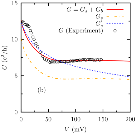
To check the quantitative agreement between the experimental results and the theoretical ones, we plot our numerical fittings to the experimental data from Ref. [Costache et al., 2014] for sample D2 under a gate voltage of V by using different parameters in Fig. 1(b). The electron density per surface is estimated to be cm-2 in the experiment at such a gate voltage. If all the electrons occupy the surface states and the bulk does not have any contribution to the charge transport, then the total conductance is the same as the surface one. Under this assumption, the surface conductance from our computation (), shown in Fig. 1(b) as dashed curve, fits reasonably well with the experimental data in the low field regime when the impurity density is cm-2. In the high field regime, however, the theoretical results deviate from the experimental ones. The theoretical saturated voltage in this case is about 200 mV, much larger than 50 mV from the experiment, and the residual conductance is about 5, 30 % smaller than the experimental one.
According to Eq. (10), to have a smaller saturated voltage, the background surface charge density should be smaller. The overall quantitative fitting can indeed be improved if some of the electrons are assumed to be populated in the bulk impurity bands.Checkelsky et al. (2011); Costache et al. (2014) In this case, the total conductance is the summation of surface conductance and the bulk one . Since the conductance of the bulk impurity bands is determined by the disorder, can be regarded as a constant that does not variate with the applied voltage in the observed regime.Checkelsky et al. (2011); Costache et al. (2014) In Fig. 1(b) we further show the total conductance for the surfaces with cm-2 and cm-2 plus a bulk contribution with a constant conductance . One finds that our numerical results are in good agreement with the experimental data for both low and high applied voltages. It is noted that we do not consider the excitation of carriers from the surface states to the bulk ones in our calculation. The charge densities on the surface and in the bulk remain constant and do not change with the applied field/voltage. Since the bulk charge density and the conductance are constant, all the variations in the transport properties are caused solely by the carriers on the surface. Our results suggest that the bulk indeed has a non-negligable contribution to the total conductance. However, the main transport phenomena, such as the incomplete current saturation and the finite residual conductance under high field, can be understood within the framework of surface transport alone without the influence of the bulk part.
In the works of Checkelsky et al.Checkelsky et al. (2011) and Costache et al.,Costache et al. (2014) the incomplete current saturation and the finite residual conductance were speculated to be associated with the excitation of the carrier from surface states to the bulk ones which have finite constant conductance. It is argued that in the experimental setup, the energy gap of Bi2Se3 can be reduced from 300 meV to about 50 meV due to the band bending, thus enabling the carriers on the surface to be excited to the bulk with an applied voltage of 50 mV. For the argument to be valid, the transport must be nearly ballistic so that the carriers in the surface states can gain enough energy to jump over the energy gap. However, in the experimental setup the mean free path is less than 30 nm. It means that the average energy gain by the carriers is less than 4 meV for an applied voltage of 50 mV over a sample with a length of 410 nm. This energy gain is too small to excite the carriers from the surface states to the bulk ones even if the energy gap is indeed reduced to 50 meV. Therefore, the excitation from the surface states to the bulk ones is very unlikely to be the main reason for the incomplete current saturation and the finite residual conductance at high voltage. From our theoretical results, the more likely reason for these high-field/voltage transport phenomena is the joint effects of the hot-electron transport and the excitation within the surface bands.
IV Conclusion
In conclusion, we have studied the charge transport on the surface of Bi2Se3 by numerically solving the KSBEs and reproduce the main qualitative features of the experimental results, i.e., the incomplete current saturation and the finite residual conductance in high applied voltage regime, without introducing any bulk contribution. Due to the hot-electron effect, the electron-phonon scattering is enhanced and leads to a reduced mobility, inversely proportional to the applied field at high field regime. As a result, the current shows tendency of saturation. On the other hand, the applied electric field can excite carriers from the surface valance band to the surface conduction one due to the interband preccession. This leads to the increase of the current carrying carriers and thus the increase of current. Under high applied voltage, the conductance approaches a finite residual value as the number of the excited carriers, being proportional to the electric field, exceeds the background one. Moreover, the theoretical results agree quantitatively well with the experimental data if a constant bulk conductance, which does not change with the applied voltage in the experimental measured regime, is introduced. This suggests that even though the bulk has a non-neglectable contribution to the the total conductance, the main transport phenomena, such as the incomplete current saturation and the finite residual conductance at high applied voltage/field, can be well understood in the framework of surface transport alone.
Acknowledgements.
This work was supported by the National Natural Science Foundation of China under Grant No. 11334014, the National Basic Research Program of China under Grant No. 2012CB922002, and the Strategic Priority Research Program of the Chinese Academy of Sciences under Grant No. XDB01000000References
- Fu et al. (2007) L. Fu, C. L. Kane, and E. J. Mele, Phys. Rev. Lett. 98, 106803 (2007).
- Zhang et al. (2009) H. Zhang, C.-X. Liu, X.-L. Qi, X. Dai, Z. Fang, and S.-C. Zhang, Nat. Phys. 5, 438 (2009).
- Xia et al. (2009) Y. Xia, D. Qian, D. Hsieh, L. Wray, A. Pal, H. Lin, A. Bansil, D. Grauer, Y. S. Hor, R. J. Cava, and M. Z. Hasan, Nat. Phys. 5, 398 (2009).
- Hsieh et al. (2009a) D. Hsieh, Y. Xia, D. Qian, L. Wray, F. Meier, J. H. Dil, J. Osterwalder, L. Patthey, A. V. Fedorov, H. Lin, A. Bansil, D. Grauer, Y. S. Hor, R. J. Cava, and M. Z. Hasan, Phys. Rev. Lett. 103, 146401 (2009a).
- Hasan and Kane (2010) M. Z. Hasan and C. L. Kane, Rev. Mod. Phys. 82, 3045 (2010).
- Hsieh et al. (2009b) D. Hsieh, Y. Xia, D. Qian, L. Wray, J. H. Dil, F. Meier, J. Osterwalder, L. Patthey, J. G. Checkelsky, N. P. Ong, A. V. Fedorov, H. Lin, A. Bansil, D. Grauer, Y. S. Hor, R. J. Cava, and M. Z. Hasan, Nature 460, 1101 (2009b).
- Analytis et al. (2010a) J. G. Analytis, R. D. McDonald, S. C. Riggs, J.-H. Chu, G. S. Boebinger, and I. R. Fisher, Nat. Phys. 6, 960 (2010a).
- Pan et al. (2011) Z.-H. Pan, E. Vescovo, A. V. Fedorov, D. Gardner, Y. S. Lee, S. Chu, G. D. Gu, and T. Valla, Phys. Rev. Lett. 106, 257004 (2011).
- Chen et al. (2009) Y. L. Chen, J. G. Analytis, J.-H. Chu, Z. K. Liu, S.-K. Mo, X. L. Qi, H. J. Zhang, D. H. Lu, X. Dai, Z. Fang, S. C. Zhang, I. R. Fisher, Z. Hussain, and Z.-X. Shen, Science 325, 178 (2009).
- Qi and Zhang (2011) X.-L. Qi and S.-C. Zhang, Rev. Mod. Phys. 83, 1057 (2011).
- Hasan and Moore (2011) M. Z. Hasan and J. E. Moore, Ann. Rev. Cond. Matt. Phys. 2, 55 (2011).
- Qi et al. (2008) X.-L. Qi, T. L. Hughes, and S.-C. Zhang, Phys. Rev. B 78, 195424 (2008).
- Fiete et al. (2012) G. A. Fiete, V. Chua, M. Kargarian, R. Lundgren, A. Rüegg, J. Wen, and V. Zyuzin, Physica E 44, 845 (2012).
- Culcer (2012) D. Culcer, Physica E 44, 860 (2012).
- Culcer et al. (2010) D. Culcer, E. H. Hwang, T. D. Stanescu, and S. Das Sarma, Phys. Rev. B 82, 155457 (2010).
- Burkov and Hawthorn (2010) A. A. Burkov and D. G. Hawthorn, Phys. Rev. Lett. 105, 066802 (2010).
- Barreto et al. (2013) L. Barreto, L. Kühnemund, F. Edler, C. Tegenkamp, J. Mi, M. Bremholm, B. B. Iversen, C. Frydendahl, M. Bianchi, and P. Hofmann, arXiv:1310.0202, (2013).
- Skinner et al. (2013) B. Skinner, T. Chen, and B. I. Shklovskii, JETP 117, 579 (2013).
- Butch et al. (2010) N. P. Butch, K. Kirshenbaum, P. Syers, A. B. Sushkov, G. S. Jenkins, H. D. Drew, and J. Paglione, Phys. Rev. B 81, 241301 (2010).
- Analytis et al. (2010b) J. G. Analytis, J.-H. Chu, Y. Chen, F. Corredor, R. D. McDonald, Z. X. Shen, and I. R. Fisher, Phys. Rev. B 81, 205407 (2010b).
- Eto et al. (2010) K. Eto, Z. Ren, A. A. Taskin, K. Segawa, and Y. Ando, Phys. Rev. B 81, 195309 (2010).
- Ren et al. (2011a) Z. Ren, A. A. Taskin, S. Sasaki, K. Segawa, and Y. Ando, Phys. Rev. B 84, 075316 (2011a).
- Ren et al. (2011b) Z. Ren, A. A. Taskin, S. Sasaki, K. Segawa, and Y. Ando, Phys. Rev. B 84, 165311 (2011b).
- Ren et al. (2012) Z. Ren, A. A. Taskin, S. Sasaki, K. Segawa, and Y. Ando, Phys. Rev. B 85, 155301 (2012).
- Checkelsky et al. (2011) J. G. Checkelsky, Y. S. Hor, R. J. Cava, and N. P. Ong, Phys. Rev. Lett. 106, 196801 (2011).
- Costache et al. (2014) M. V. Costache, I. Neumann, J. F. Sierra, V. Marinova, M. M. Gospodinov, S. Roche, and S. O. Valenzuela, Phys. Rev. Lett. 112, 086601 (2014).
- Zhang and Wu (2013) P. Zhang and M. W. Wu, Phys. Rev. B 87, 085319 (2013).
- Bychkov and Rashba (1984) Y. A. Bychkov and E. I. Rashba, J. Phys. C 17, 6039 (1984).
- Liu et al. (2010) C.-X. Liu, X.-L. Qi, H. Zhang, X. Dai, Z. Fang, and S.-C. Zhang, Phys. Rev. B 82, 045122 (2010).
- Fu (2009) L. Fu, Phys. Rev. Lett. 103, 266801 (2009).
- Richter and Becker (1977) W. Richter and C. R. Becker, Phys. Stat. Sol. (B) 84, 619 (1977).
- Giraud and Egger (2011) S. Giraud and R. Egger, Phys. Rev. B 83, 245322 (2011).
- Giraud et al. (2012) S. Giraud, A. Kundu, and R. Egger, ibid. 85, 035441 (2012).
- Zhu et al. (2011) X. Zhu, L. Santos, R. Sankar, S. Chikara, C. . Howard, F. C. Chou, C. Chamon, and M. El-Batanouny, Phys. Rev. Lett. 107, 186102 (2011).
- Shoemake et al. (1969) G. E. Shoemake, J. A. Rayne, and R. W. Ure, Phys. Rev. 185, 1046 (1969).
- Wiese and Muldawer (1960) J. Wiese and L. Muldawer, Journal of Physics and Chemistry of Solids 15, 13 (1960).
- Fu and Kane (2007) L. Fu and C. L. Kane, Phys. Rev. B 76, 045302 (2007).
- Haug and Jauho (1996) H. Haug and A.-P. Jauho, Quantum Kinetics in Transport and Optics of Semiconductors (Springer, Berlin, 1996).
- Wu et al. (2010) M. W. Wu, J. H. Jiang, and M. Q. Weng, Phys. Rep. 493, 61 (2010).
- Cheng and Wu (2006) J. L. Cheng and M. W. Wu, J. Appl. Phys. 99, 083704 (2006).
- Balev et al. (2009) O. G. Balev, F. T. Vasko, and V. Ryzhii, Phys. Rev. B 79, 165432 (2009).
- Weng et al. (2004) M. Q. Weng, M. W. Wu, and L. Jiang, Phys. Rev. B 69, 245320 (2004).
- Barreiro et al. (2009) A. Barreiro, M. Lazzeri, J. Moser, F. Mauri, and A. Bachtold, Phys. Rev. Lett. 103, 076601 (2009).
- Yao et al. (2000) Z. Yao, C. L. Kane, and C. Dekker, Phys. Rev. Lett. 84, 2941 (2000).