Copyright (2014) American Institute of Physics. This article may be downloaded for personal use only. Any other use requires prior permission of the author and the American Institute of Physics.
The following article appeared in J. Appl. Phys. 115 203102 (2014) and may be found at http://dx.doi.org/10.1063/1.4878939
Composition determination of quaternary GaAsPN layers from single XRD measurement of quasi-forbidden (002) reflection
Abstract
GaAsPN layers with a thickness of 30nm were grown on GaP substrates with metalorganic vapor phase epitaxy to study the feasibility of a single X-ray diffraction (XRD) measurement for full composition determination of quaternary layer material. The method is based on the peak intensity of a quasi-forbidden (002) reflection which is shown to vary with changing arsenic content for GaAsPN. The method works for thin films with a wide range of arsenic contents and shows a clear variation in the reflection intensity as a function of changing layer composition. The obtained thicknesses and compositions of the grown layers are compared with accurate reference values obtained by Rutherford backscattering spectroscopy combined with nuclear reaction analysis measurements. Based on the comparison, the error in the XRD defined material composition becomes larger with increasing nitrogen content and layer thickness. This suggests that the dominating error source is the deteriorated crystal quality due to the nonsubstitutional incorporation of nitrogen into the crystal lattice and strain relaxation. The results reveal that the method overestimates the arsenic and nitrogen content within error margins of about 0.12 and about 0.025, respectively.
pacs:
61.05.cp, 68.55.-a, 82.80.YcI Introduction
GaAsyP1-x-yNx is an interesting material with many potential applications. The incorporation of As and N into this material reduces the band gap and changes the indirect band gap of GaP to a direct one, enabling the fabrication of optoelectronic components on GaP substrates. As the lattice constant of GaP is very close to that of silicon, with a high-quality buffer layer it is also possible to fabricate these components on top of silicon platforms. As a matter of fact, an electrically pumped semiconductor laser of GaAsPN quantum wells monolithically integrated on silicon has already been demonstratedLiebich et al. (2011). Furthermore, GaAsPN has recently drawn increasing amount of attention also in the solar cell research community. For instance, GaAsPN has been proposed as a material to be used in the fabrication of a silicon tandem solar cellAlmosni et al. (2013). In addition to this, the nitrogen present in this material splits the conduction band into twoYu et al. (2006), potentially allowing the fabrication of an intermediate-band solar cellLópez et al. (2011).
However, the composition determination of quaternary materials remains a challenge. X-ray diffraction (XRD)Bartels (1983); Fewster (1993) is a commonly used method to determine the composition of compound semiconductors. The method is based on determining the location of the XRD peak, but it does not directly allow full composition determination of quaternary semiconductors. As an example of the challenges, the composition of the GaAsPN layer in the aforementioned silicon laser was ”estimated by the strain state in line with various test structures investigating the incorporation behavior of the different elements in MOVPE”Liebich et al. (2011). A second free variable, such as determination of the band gap energy, is typically required for full composition determination.
Previously, it has been demonstrated that the peak intensity of a quasi-forbidden reflection varies strongly as a function of material composition for InAlAsSbWallis et al. (2001). In this work, it is shown that the peak intensity of the quasi-forbidden (002) XRD reflection of GaAsPN also varies strongly with arsenic content. This factor is held as a second free variable and used to determine the material composition. The obtained compositions and layer thicknesses are compared to accurate reference values obtained with Rutherford backscattering spectroscopy (RBS) combined with nuclear reaction analysis (NRA) measurements.
II Experimental details
The samples studied in this paper were grown with metalorganic vapor phase epitaxy (MOVPE) at atmospheric pressure. The used precursors were trimethylgallium (TMGa), tertiarybutylarsine (TBAs), tertiarybutylphosphine (TBP) and dimethylhydrazine (DMHy) for gallium, arsenic, phosphorus and nitrogen, respectively. The GaAsPN layers were grown directly on top of GaP (001) substrates. The growth temperature was and the samples were subsequently annealed for 5 minutes at . Nominally 130 nm thick GaAsPN layers (samples #6 - #9) were grown with similar flows as the 30 nm thick layers (samples #5, #4, #1 and #2, respectively) for RBS/NRA measurements. The used V/III ratio for the samples was about 100 but varied slightly for each sample. The information about the sample growth relating to the used V/III, TBAs/V and DMHy/V ratios is found in Table 2.
The strain state, crystallographic plane tilt, composition and thickness of the grown layers were studied with a commercial Philips X’Pert Pro MRD diffractometer. The measurement was performed in a high resolution mode using a Ge (220) monochromator and an X-ray mirror at the incident beam side and an analyzer crystal at the diffracted beam side. We also performed similar measurements with an open detector at the diffracted beam side, but the measured curve did not correspond to the simulated curve that well and the accuracy of the method was worse.
Results from the XRD measurements were obtained with fitting analyses made with a custom XRD curve fitting softwareTilli (2007) that utilized dynamical diffraction theory. The calculated electric susceptibilities and XRD curves and values obtained with the fitting analysis with the custom software have been compared with other software and found to be in good agreement. It should be noted that the used deviation parameter formulaBartels, Hornstra, and Lobeek (1986) may not be accurate with highly mismatched epitaxial structures, so we tested simulated curves of a GaAsPN layer against Sergey Stepanov’s X-ray server at http://x-server.gmca.aps.anl.gov/, which uses a recursive matrix approach of dynamical X-ray diffractionStepanov et al. (1998). The simulated curves were almost identical, and the intensity of the thin film peak when compared to the substrate peak was the same. Note that any XRD curve fitting software works with the used quaternary composition determination method, as long as the value of the fitting error is exposed to the user. Table 1 lists the Poisson’s ratios, lattice constants and Debye-Waller -factors of different elements required for calculation of the simulated XRD curve. Note that the -factors for P and N were missing and a value of 0 was used instead. However, as the values for the Debye-Waller factor, i.e. , for Ga and As are 0.984 and 0.981, respectively, the effect of the Debye-Waller -factor on the calculated electric susceptibility is small and therefore the missing values for P and N can be assumed not to significantly alter the calculated electric susceptibiliy value.
| Material | parameter | value |
|---|---|---|
| GaP | Poisson’s ratio | 0.3070 |
| GaAs | Poisson’s ratio | 0.311 |
| cubic GaN | Poisson’s ratio | 0.33 |
| GaP | lattice constant | 5.4505 Å |
| GaAs | lattice constant | 5.65368 Å |
| cubic GaN | lattice constant | 4.5034 Å |
| Ga | Debye-Waller -factor | 0.46675 Å2 |
| As | Debye-Waller -factor | 0.55504 Å2 |
RBS and NRA measurements were performed for all the samples in order to get accurate reference values for the layer thicknesses and compositions. Compositions of the films were measured by channeling Rutherford backscattering spectroscopy (c-RBS) together with nuclear reaction analysis (NRA). The 14N(,p)17O reaction with a 3.72 MeV 4He2+ beam was used for detection of nitrogen. A 150 mm2 passivated implanted planar silicon (PIPS) detector with a 312 mm slit was used to detect the emitted protons at with respect to the incident beam. A thick mylar foil was placed in front of the detector to absorb the backscattered alpha particles. RBS spectra were also obtained simultaneously at with another PIPS detector. Both RBS and NRA measurements were carried out in random and 100 axial channeling directions. The fraction of substitutional nitrogen atoms in the films was obtained by comparing the random and channeling yields of the RBS and the NRA measurements.
III Theory
As previously described, the use of the location of an XRD peak allows composition determination of only ternary semiconductors, as only one free composition-related variable, the lattice constant, can be deduced from the peak location. Therefore, a second variable needs to be known to determine the composition of quaternary compounds. The second variable gathered by standard XRD diffractometer could for example be electron density determined by X-ray reflectivity (XRR). However, it should be noted that it has been previously estimated that the relative accuracy of the density determination for ALD-grown Al2O3 on silicon is on the order of 3.5%Tiilikainen et al. (2007, 2008). Since Al2O3 on Si has a significantly better electron density contrast when compared to GaAsPN on GaP, using electron density determined by XRR as the second free variable with GaAsPN is expected to have a significantly lower accuracy and hence does not seem to be feasible.

Instead, the intensity of the XRD reflection is used in this work as the second free variable for the definition of the material composition. To demonstrate the effect, the XRD spectra of the allowed (004) and the quasi-forbidden (002) reflection are simulated for a 75 nm thick GaAsPN layer on a GaP substrate as a function of changing arsenic content. These XRD spectra are shown in figures 1 and 2. In the figures, the arsenic content is varied with the lattice constant being kept constant by varying also the nitrogen content. Note that some of the curves are unphysical, i.e., it is assumed that all of the layers are fully strained and that the nitrogen content needed to keep the lattice constant the same is unrealistically high in some of the curves. It can be seen from the figure that the intensity of the allowed (004) reflection does not vary enough to be able to make deductions about the composition based on the reflection intensity. However, for the quasi-forbidden (002) reflection the intensity of the XRD peak varies strongly as a function of the material composition. This occurs because for GaAs, the scattering factors for Ga (31 electrons) and As (33 electrons) are very close to each other. As a result of this, the interference from Ga and As atoms is nearly but not completely destructive for the (002) reflection giving rise to a non-zero structure factor. Additionally, replacing a certain small fraction of As atoms (about 10%) with P (15 electrons) causes the interference to be completely destructive and replacing more of the As atoms with P causes the interference to be less destructive. Note also that the same is true for the (006) reflection.
The composition can be determined from the peak location and intensity using two different methods. One possibility is comparing the integrated intensity of the thin film peak with the substrate peak. This has been previously used to determine the composition of quaternary InAlAsSbWallis et al. (2001). Another possibility is with an automatic fitting analysis. The advantage of the fitting analysis over the integrated intensity method is that the fitting analysis works for materials having a lattice constant closely matched to the substrate, as the peaks of the substrate and the grown layer can be fused together. Such was the case in our sample #5.
The available curve-fitting software typically allows fitting only one composition-related parameter. Here a semiautomatic fitting analysis was used. The As content was set to a fixed trial value and the fitting analysis was performed with the fitting parameters being the N content, the layer thickness, the intensity normalization factor and a correction offset for the diffraction angle. The minimum possible value of the fitting error was recorded for every trial As content and the value which minimizes the fitting error was manually determined by drawing a graph of the minimum possible values of the fitting error as a function of the As content. The used fitting error was obtained by calculating the 2-norm in logarithmic space.
It was found that using the peak intensity is not as accurate as using the peak position in determining the composition of the material. In particular, the following sources of error may be present:
-
(i)
Poisson-distributed photon counting noise. This can result in the determined arsenic content being either too high or too low. This error source is random and can be reduced by using longer photon counting times. The magnitude of this error source may be estimated by performing the measurement multiple times and doing the fitting analysis for each measurement separately.
-
(ii)
If the crystal planes of the thin film are tilted, the true peak may be at a different or angle relative to the peak of the substrate. This results in the peak observed in an 1-axis scan being weaker than the true peak. The result is that the determined arsenic content is too high.
-
(iii)
If the crystal quality of the layer is not good, the peak will be weaker than predicted by the theory. This error source will also result in the determined arsenic content being too high.
-
(iv)
The layer may be partially relaxed. In this case, assuming the layer is compressively strained, the determined nitrogen level is too high, as both relaxation and an increase in nitrogen content tend to move the peak to a higher angle. The relaxation may be studied with asymmetric reflections and the relaxation can be eliminated by ensuring that the layer thickness is below the critical thickness.
-
(v)
Inaccuracies in the used atomic scattering factors can also affect the results. As long as the used atomic scattering factors are reasonably close to the real values, the effect of the peak intensity varying as a function of the arsenic content can be seen. However, if they are slightly incorrect, the magnitude of the effect in simulations will change.
-
(vi)
Inaccuracies in the Poisson’s ratios and the lattice constants (Table 1) can affect the results, but they affect mainly the determined N content and not the electric susceptibilities which determine the peak intensity and thus the As content. Theoretically, inaccuracies in the Debye-Waller -factors might also affect the calculated electric susceptibilities somewhat, but as is over 0.98 for the values of we used, the effect of the Debye-Waller -factors is expected to be insignificant.
It should also be noted that there is crosserror between the determined arsenic content and the determined nitrogen content. If, e.g., due to one of the aforementioned error sources the arsenic content determined from the peak intensity is too high, this would move the peak to a lower angle without an increase in the nitrogen content. The fitting analysis will then find also the nitrogen content that is too high.
IV Results and discussion
IV.1 Full composition determination from a single XRD measurement
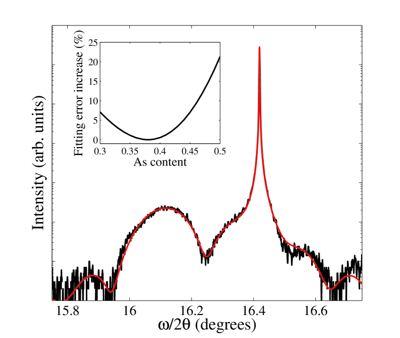
The full compositions of the samples were determined with a single XRD scan of the (002) reflection. A simulated model was fitted to the measured data with the method presented earlier. Excellent fits were obtained which is illustrated in figure 3 for sample #1. The inset of figure 3 shows the obtained relative fitting error as a function of the trial As content. The relative fitting error, which is presented with respect to the minimum fitting error, changes significantly and shows a clear minimum with the As content of 38 %. Therefore, with the measurement of a single XRD curve of the quasi-forbidden (002) reflection, it is possible with high precision to unambigously define the layer composition of the quaternary material.
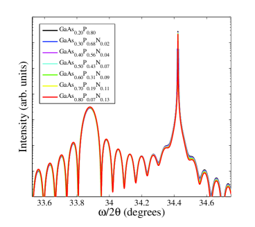
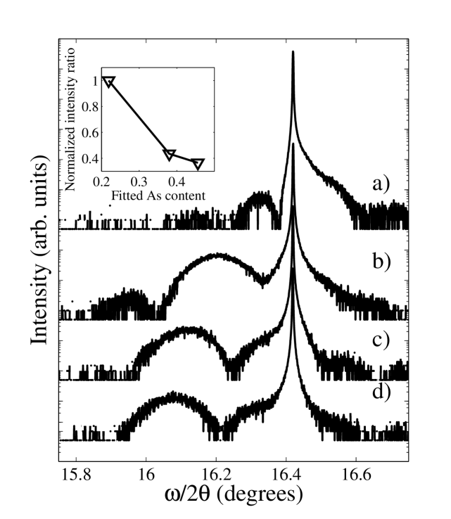
The fits to the other measurements (not shown) were equally good and other measurements had similarly a distinct variation of the fitting error as a function of the arsenic content. The measured XRD curves from samples #1, #2, #4 and #5 are shown together in figure 4 illustrating the variation of the peak intensity for samples with different composition. The XRD curve of sample #3 having a similar arsenic content as sample #2 is not shown. It should be noted that as sample #5 had no arsenic, the peak of the layer is on the right side of the substrate and is fused together with the substrate peak in this case. The small peak seen on the left is an interference effect. The inset of figure 4 shows the intensity ratios of the layer and the substrate peaks and clearly demonstrates that the reflection intensity variation seen in simulations (figure 2) occurs also in the XRD measurements of real samples.
The determined compositions and thicknesses of the grown layers are shown in Table 2. It should be noted that the determined nitrogen content seems to vary a lot depending on the arsenic content even though the DMHy/V ratios used for all of the samples were similar. In addition, one interesting observation is that no difference could be seen in the nitrogen contents of samples #2 and #3 grown with different DMHy/V flows. This can be explained by the fact that using the peak intensity is not as accurate in determining composition as using the peak location and that there is the previously mentioned crosserror between the determined arsenic and nitrogen contents. This fact can be illustrated by forcing the arsenic content of sample #2 to be 0.439, the same as sample #3. This causes the fitting analysis to find a nitrogen content of 0.027 for sample #2 in contrast to the value of 0.031 which was obtained using the method described in this paper. In addition to this, it is observed that the fitting analysis of the samples #5 and #6 grown with no arsenic flow gives an arsenic content larger than zero which is unrealistic because it is known that these grown layers cannot contain any arsenic. Theoretically, some As could be present in the reactor from previously grown samples, but our RBS measurements demonstrate that these layers did not contain any arsenic. Additionally, it would be very unlikely that so much As would be incorporated into a grown sample from impurities present in the reactor, so the determined As content is due to a systematic error source in the composition determination method and not due to the samples having real As.
It can also be seen that for most samples, XRD underestimates the layer thickness. This is likely caused by the fact that the measured (002) XRD curves of especially the 130 nm thick layers did not have notable interference fringes and thus the layer thickness was determined from the width of the XRD peak. It is likely that the crystal quality of these samples had been deteriorated due to increased strain which caused the XRD peaks to broaden and lead the fitting to reveal a lower thickness than the actual thickness.
| Sample | Growth parameter | Thickness | Composition | ||||
|---|---|---|---|---|---|---|---|
| V/III | DMHy/V | TBAs/V | nominal | measured | |||
| #1 | 101 | 0.32 | 0.045 | 30 nm | 29.5 nm | 0.380 | 0.022 |
| #1 (a | 29.1 nm | 0.374 | 0.020 | ||||
| #2 | 103 | 0.32 | 0.061 | 30 nm | 27.7 nm | 0.456 | 0.031 |
| #3 | 106 | 0.39 | 0.054 | 30 nm | 28.2 nm | 0.439 | 0.030 |
| #4 | 100 | 0.30 | 0.020 | 30 nm | 29.6 nm | 0.219 | 0.004 |
| #5 | 98 | 0.31 | 0.000 | 30 nm | 28.3 nm | 0.082 | 0.025 |
| #6 | 101 | 0.32 | 0.000 | 130 nm | 132.5 nm | 0.229 | 0.058 |
| #7 | 103 | 0.32 | 0.020 | 130 nm | 99.7 nm | 0.693 | 0.119 |
| #8 | 101 | 0.32 | 0.046 | 130 nm | 62.3 nm | 0.787 | 0.120 |
| #9 | 103 | 0.32 | 0.061 | 130 nm | 64.7 nm | 0.776 | 0.110 |
IV.2 RBS and NRA measurements
| Sample | RBS/NRA | XRD | |||||
|---|---|---|---|---|---|---|---|
| Thickness | |||||||
| #1 | 31 nm | 0.31 | ? | 0.007 | |||
| #2 | 31.5 nm | 0.34 | ? | 0.006 | |||
| #3 | 31 nm | 0.32 | ? | 0.004 | |||
| #4 | 31 nm | 0.22 | ? | 0.004 | |||
| #5 | ? | 0 | ? | 0.006 | |||
| #6 | 120 nm | 0 | 0.016 | 0.06 | 0.19 | 0.86 | 0.008 |
| #7 | 124 nm | 0.2 | 0.013 | 0.09 | 0.16 | 0.92 | 0.012 |
| #8 | 125 nm | 0.31 | 0.008 | 0.017 | |||
| #9 | 120 nm | 0.32 | 0.01 | 0.012 | |||
In order to estimate the accuracy of the XRD measurement results, RBS and NRA measurements were performed for all the samples. The results of the measurements are shown in Table 3. Note that NRA measurements on the thin samples (30 nm) were not performed because the N signals were too low to determine the N content in these cases. The thicknesses of the films were estimated by assuming an average atomic composition of the film from the measured As content and, therefore, are accurate to about 5%. For the thicker GaAsPN layers, NRA results were fitted by the SIMNRA software Mayer (1999) using a thin InN thin film as a standard for N quantification. The accuracy of the N measurements in these cases is within 10%. Note that for a perfect crystal the GaAsPN minimum yield (), ratio of the channeling to the random yields, should be on the order of 0.04. However, for sample #6 and #7 are significantly higher than that. This suggests that extended defect density in these samples (particularly sample #7) is significantly higher giving rise to a higher dechanneling of the ion beam.
To investigate how well the RBS and NRA determined As and N contents agree with XRD measurements, we determined the N contents with XRD analysis by forcing the As content to be the RBS-determined value instead of using the described quaternary fitting method. The results are also shown in the right-most column of Table 3. It can be seen that for the samples #6 and #7 the XRD determined N contents are smaller than the values determined by NRA. This is consistent with earlier experimentsJussila et al. (2014) that the determined N content is too low, as Ga(As)PN may not exactly obey Vegard’s law. However, for samples #8 and #9 the XRD determined N content is higher than the NRA determined value. This is consistent with partial relaxation of the layers.
IV.3 Error sources
The XRD defined material compositions deviate significantly from the reference values obtained by the RBS/NRA measurements. To explain the differences, the magnitude of different error sources potentially present in the XRD analysis was estimated.
IV.3.1 Photon counting noise
To get an estimate how the photon-counting noise and other measurement-related inaccuracies affect the determined composition, the XRD curve for sample #1 was measured twice and the fitting analysis was performed separately for each measurement. From the two measurements, it can be seen that the precision of the method has absolute errors of about 0.006 and 0.002 for As and N contents, respectively. Thus, the photon counting noise is not a significant error source for the analysis. This is the case even though the intensity of the GaAsPN peak (below 100 counts) is significantly smaller than the intensity of reported in the previous study for InAlAsSbWallis et al. (2001). Additionally, measurement repeatability was simulated by using the simulated curve from GaAs0.380P0.598N0.022 as the fitting target after adding simulated Poisson-distributed noise to it. This was done five times and the determined compositions are listed in Table 4. Thus, even though the statistics was not significant, i.e., we repeated the measurement only twice for one sample and did the measurement repeatability test five times, the results suggest that the photon counting noise error source is not significant in the analysis. Note that there may always be also other measurement reproducibility error sources such as sample misalignment.
| Fitting run | ||
|---|---|---|
| 1 | 0.375 | 0.021 |
| 2 | 0.377 | 0.022 |
| 3 | 0.375 | 0.021 |
| 4 | 0.374 | 0.021 |
| 5 | 0.380 | 0.022 |
IV.3.2 Crystallographic tilt and strain
It has been assumed in the XRD fitting analysis that the crystal planes parallel to the surface of the thin film are not tilted differently from the substrate and that the thin film is fully strained. Either crystal plane tilt or relaxation can result in systematic errors in the measurement. Relaxation occurs for all layers of material different from the substrate when the critical thickness is exceeded and it has been shown that a GaP layer grown on a misoriented silicon surface can relieve its strain energy by tilting the crystal planesTakagi et al. (2010). Therefore, it is important to check that the layer is fully strained and that the crystal planes are not tilted, although it should be noted that crystallographic tilt is extremely improbable when the layer is grown on a nominally exactly cut wafers. The tilting of the crystal planes was studied with a reciprocal space map of the symmetric (004) reflection. The reciprocal space maps (not shown) indicate that for all of the 30 nm thick samples, the true thin film XRD peak occurs at the same offset angle as the substrate peak with an accuracy of . Therefore, the crystal planes are not tilted.

The relaxation of the layer was studied with a reciprocal space map of the asymmetric (113) reflection. All of the reciprocal space maps for the 30 nm thick layers indicate that the layer peak occurs at the same value of the diffraction vector component along the crystal plane, , as the substrate peak and, thus, the layers are fully strained. The reciprocal space map of the (113) reflection of sample #1 is shown in figure 5. Reciprocal space maps were not measured for 130 nm thick samples. However, assuming similar discrepancy between the experimentally measured and theoretically calculated critical thickness as reported for the GaP0.98N0.02 layers on GaP substrateJussila et al. (2013), the critical thickness of the GaAsPN layer in samples #6, #7, #8, and #9 can be estimated to be on the order of 175 nm, 140 nm, 60 nm and 60 nm, respectively. Thus it is likely that at least samples #8 and #9 were partially relaxed.
IV.3.3 Impact of the layer thickness
As explained in chapter IV.1, for all of the nominally 130 nm thick samples the determined arsenic content was much higher than for the 30 nm thick samples grown with similar precursor flows. This can be explained by the lower crystalline quality of the thicker films due to increased lattice strain as the epilayer in none of the samples was lattice matched to the GaP substrate. The presence of lattice strain creates crystalline defects which causes the XRD peak to be weaker and broader than that predicted by theory. This is in agreement with the high channeling yield shown for these layers. This results in several effects:
-
(i)
The determined arsenic content is too high, because high arsenic content and a low crystalline quality both result in a weak XRD peak.
-
(ii)
The determined nitrogen content is too high due to two reasons: the layer may be relaxed, and there is a crosserror between the determined arsenic content and the determined nitrogen content. Additionally, relaxation may explain the broad and weak peak shapes observed and the determined low thickness values.
-
(iii)
The determined thickness is too low, as the XRD curves did not have notable interference fringes and, thus, the layer thickness was determined from the width of the XRD peak. Relaxation causes the peaks to be broader than predicted by the dynamical diffraction theory, and thus the determined thickness will be too low.
Based on this discussion, it can be concluded that the aforementioned error sources are the smallest if the layer is as thin as possible. However, at the same time there is a trade-off because if the layer is very thin, the XRD peak is wide and weak, which makes fitting analysis harder. The set of 130nm thick samples had bad structural quality due to reasons explained before, and therefore, is not very useful from the XRD measurement point of view.
IV.4 Failure of the simulation to reproduce the experimental intensity
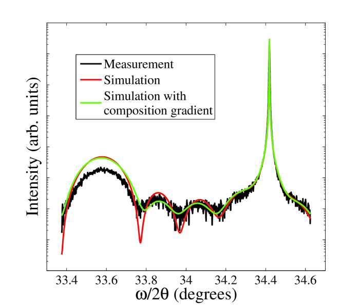
From the comparison between the XRD and RBS/NRA results, it is known that the XRD based method overestimates the arsenic content. Therefore, it seems to be the case, simply judging from this fact, that the XRD peaks are weaker than the theory predicts. To demonstrate this issue the (004) XRD reflection of sample #2 and the simulated XRD curve are shown in figure 6. Note that the intensity of this reflection does not depend on the material composition. It can be observed that the angular region in the measured XRD curve that originates from the crystal planes of the GaAsPN epilayer produces a weaker intensity than what the theory predicts. In the previous study of InAlAsSb alloyWallis et al. (2001), this observation has been called ”failure of the simulation to reproduce the experimental intensity” with no possible explanations given other than inaccuracies in the used atomic scattering factors. However, it can be deduced based on the comparison between the different methods that the arsenic content does not seem to be off by the same amount in all of the samples. Therefore, the weak intensity is not likely originating from errors in the atomic scattering factors.
Another possible reason for the weakness of the peaks might be a compositional gradient inside the GaAsPN layer. Note that all the samples were annealed in-situ for 5 minutes to enhance the substitutionality of N into the alloy. During the anneal, however, no DMHy was flown inside the reactor which may cause that due to desorption the N content of the layer can be lower near the surface of the layer. Therefore, this hypothesis was tested fitting a sample model with two layers of GaAsPN with one having a smaller N content than the other. A simulation for the two layer model is also shown in figure 6. It can be seen that in this case the intensity of the interference fringes agrees better to the experimentally measured XRD curve but the intensity level of the XRD peak of the layer is still similarly too high. Thus, a compositional gradient is not the only source of discrepancy between the measurements and the dynamical theory, and therefore, we believe that the most straightforward explanation for the weakness of the experimentally measured XRD peak is the presence of crystalline defects inside the GaAsPN layer.
A possible explanation for why the systematic error here is larger than previously found is that nitrogen atoms can occupy interstitial sites in the crystal lattice. For instance, it has been previously determined by RBS studies combined with NRA measurements that with the nitrogen content of GaPN increasing from 0.017 to 0.04 the substitutionality of the nitrogen decreases from 0.91 to an unresolved value due to deteriorated crystal qualityJussila et al. (2014). Thus, it is likely that the samples studied in this work contain nitrogen related point defects as well. In addition, it should be noted that for a layer with a nitrogen content of 0.036, an incorrect value of 0.02 was obtained by XRD using Vegard’s law. This difference was also explained by different nitrogen configurations other than substitutional incorporation of nitrogen into the crystal lattice affecting differently to the lattice constant.Jussila et al. (2014) The samples used in this study were grown with the same MOVPE apparatus. Furthermore, it should be noted that it has also been observed for other dilute nitride materials as well that the lattice constant may deviate significantly from Vegard’s law due to non-substitutional incorporation of N into the crystal latticeKrier et al. (2012).
The interstitial N atoms, depending on their configuration, i.e., isolated interstitials or split interstitials or other vacancy-interstitial complexes may change the lattice constant in a different way and also additionally cause strain fields around them, which affects the reflected intensity. In the models used it is assumed that no nitrogen atoms occupy interstitial sites, which is false in the real life. The substitutional fraction which was determined for samples #6 and #7 gives further support to the hypothesis that crystalline defects are the cause of the weakness of the XRD peaks. Based on the determined substitutional fraction, it can be seen that part of the nitrogen atoms are non-substitutionally incorporated into the crystal lattice. More support to this explanation was given by growing a sample with a zero arsenic content and a significantly higher nitrogen content. The determined arsenic content using the new method increased even further for this sample even though the sample contained no arsenic. In this case the agreement between the simulated curve and the measured curve was significantly worse. Thus, the systematic error increases with increasing nitrogen content and seems to be higher than the error due to measurement repeatability.
For the 30nm thick samples, we can estimate the level of systematic error from the comparison between the RBS and the XRD measurements. The level of systematic error for the arsenic content is 0.12. The systematic error in nitrogen content can be estimated by forcing the RBS-determined As content in XRD fitting analysis and determining the N content. For example, for sample #2 if we assume the As content of 0.34 in the fitting analysis, we obtain an N content of 0.006, so the level of systematic error in N content is 0.025.
IV.5 Methods to minimize inaccuracies
There are at least a few ways to improve the inaccuracies caused by crystalline defects. First, the ratio of the integrated intensity of the thin film peak to the substrate peak is calculated for both the (002) and (004) reflections. The ratio of these ratios can be compared with simulations of different As contents, and the As content for which the ratio of ratios for the measurement matches the simulation is taken to be the correct As content. However, such methods work better with the integrated peak intensity method presented earlierWallis et al. (2001) and cannot be used easily with the fitting analysis based method, which is the method that was demonstrated in this paper.
A more accurate dynamical theory of XRD which takes into account the effect of crystalline defects in the thin film would be a more comprehensive way to approach the problem. However, developing such a new theory of XRD is out of the scope of this work. It should be noted that the effect of the weakness of the XRD peak could be accounted for by multiplying the X-ray electric susceptibility of the thin film by a certain factor (the same for (002) and (004) reflections), which tends to make the thin film peak weaker. Such a factor could be determined by fitting analysis from a measured (004) XRD curve. However, such a multiplicative factor is not consistent with the dynamical X-ray diffraction theory so the proposed solution is not completely satisfactory. It can be speculated that by accounting this ”failure of the simulation to reproduce the experimental intensity” error source in the fitting procedure the accuracy of the method would approach the limits explained in the chapter IV.3.1. Such methods to improve the inaccuracies presented here have not been studied here in detail and require further work.
V Conclusions
It was shown that the intensity of the quasi-forbidden (002) reflection of GaAsPN varies strongly with arsenic content. Samples with thicknesses of 30 nm and 130 nm and different compositions were grown on GaP substrates and were measured with the designed XRD-based method and compared to accurate reference values obtained by RBS combined with NRA measurements. It was observed that the XRD-based method could unambigously determine material composition from a single scan of the (002) reflection with high precision, but the accuracy of the method for this set of samples was not good. Based on the comparison between the different measurement methods, the error in the XRD defined material composition became larger with increasing nitrogen content and layer thickness. This suggested that the dominating error source was the deteriorated crystal quality due to the nonsubstitutional incorporation of nitrogen into the crystal lattice and strain relaxation affecting the reflection intensity unexpectedly. More support for the conclusion that crystal quality was deteriorated was obtained from the high channeling yield of the RBS/NRA measurements. We also could find evidence of a compositional gradient of N from the fringe modulation in a measurement of the (004) reflection, but this did not explain the weakness of the main XRD peak. For 30 nm thick films the systematic error limits were about 0.12 for the determined arsenic content and 0.025 for the determined nitrogen content. It was proposed that the accuracy of the XRD-based method can be significantly further enhanced possibly to the limit set by typical error sources (photon counting noise, sample misalignment, etc.). This, however, requires a XRD fitting software designed in such a way that it is capable to take into account deteriorated crystal quality. In addition, a similar method could be used, in theory, for many other quaternary compound semiconductor materials.
However, when applying the presented method for quaternary composition determination, care should be taken to ensure that the layers have a sufficient crystalline quality. Note that the simple method of determining ternary layer composition from the location of the XRD peak works well for samples of even low crystalline quality, but the same is not true for determining quaternary material composition from the location and the intensity of the XRD peak. The crystalline quality can be e.g. checked by performing measurements for the (004) reflection and ensuring that the dynamical theory reproduces the experimental peak intensity.
References
- Liebich et al. (2011) S. Liebich, M. Zimprich, A. Beyer, C. Lange, D. J. Franzbach, S. Chatterjee, N. Hossain, S. J. Sweeney, K. Volz, B. Kunert, and W. Stolz, Applied Physics Letters 99, 071109 (2011).
- Almosni et al. (2013) S. Almosni, C. Robert, T. Nguyen Thanh, C. Cornet, A. Létoublon, T. Quinci, C. Levallois, M. Perrin, J. Kuyyalil, L. Pedesseau, et al., Journal of Applied Physics 113, 123509 (2013).
- Yu et al. (2006) K. M. Yu, W. Walukiewicz, J. W. Ager, D. Bour, R. Farshchi, O. D. Dubon, S. X. Li, I. D. Sharp, and E. E. Haller, Applied Physics Letters 88, 092110 (2006).
- López et al. (2011) N. López, L. A. Reichertz, K. M. Yu, K. Campman, and W. Walukiewicz, Physical Review Letters 106, 28701 (2011).
- Bartels (1983) W. J. Bartels, Journal of Vacuum Science & Technology B: Microelectronics and Nanometer Structures 1, 338 (1983).
- Fewster (1993) P. F. Fewster, Semiconductor science and technology 8, 1915 (1993).
- Wallis et al. (2001) D. J. Wallis, A. M. Keir, M. T. Emeny, and T. Martin, IEE Proceedings - Optoelectronics 148, 97 (2001).
- Tilli (2007) J.-M. Tilli, XRD fitting analysis of semiconductor heterostructures, Puolijohderakenteiden röntgendiffraktion sovitusanalyysi (in Finnish), B.Sc. thesis, Helsinki University of Technology (2007).
- Bartels, Hornstra, and Lobeek (1986) W. J. Bartels, J. Hornstra, and D. J. W. Lobeek, Acta Crystallographica A42, 539 (1986).
- Stepanov et al. (1998) S. A. Stepanov, E. A. Kondrashkina, R. Koehler, D. V. Novikov, G. Materlik, and S. M. Durbin, Physical Review B 57, 4829 (1998).
- Tiilikainen et al. (2007) J. Tiilikainen, J.-M. Tilli, V. Bosund, M. Mattila, T. Hakkarainen, J. Sormunen, and H. Lipsanen, Journal of Physics D: Applied Physics 40, 7497 (2007).
- Tiilikainen et al. (2008) J. Tiilikainen, M. Mattila, T. Hakkarainen, and H. Lipsanen, Journal of Physics D: Applied Physics 41, 115302 (2008).
- Mayer (1999) M. Mayer, in AIP conference proceedings, Vol. 475 (1999) p. 541.
- Jussila et al. (2014) H. Jussila, K. M. Yu, J. Kujala, F. Tuomisto, S. Nagarajan, J. Lemettinen, T. Huhtio, T. O. Tuomi, H. Lipsanen, and M. Sopanen, Journal of Physics D: Applied Physics 47, 075106 (2014).
- Takagi et al. (2010) Y. Takagi, Y. Furukawa, A. Wakahara, and H. Kan, Journal of Applied Physics 107, 063506 (2010).
- Jussila et al. (2013) H. Jussila, S. Nagarajan, S. Sintonen, S. Suihkonen, A. Lankinen, T. Huhtio, C. Paulmann, H. Lipsanen, T. O. Tuomi, and M. Sopanen, Thin Solid Films 534, 680 (2013).
- Krier et al. (2012) A. Krier, M. de la Mare, P. J. Carrington, M. Thompson, Q. Zhuang, A. Patanè, and R. Kudrawiec, Semiconductor Science Technology 27, 094009 (2012).