Currently with ]Intel Corporation, Hillsboro, OR
Ultrathin GaN Nanowires: Electronic, Thermal, and Thermoelectric Properties
Abstract
We present a comprehensive computational study of the electronic, thermal, and thermoelectric (TE) properties of gallium nitride nanowires (NWs) over a wide range of thicknesses (3–9 nm), doping densities (– cm-3), and temperatures (300–1000 K). We calculate the low-field electron mobility based on ensemble Monte Carlo transport simulation coupled with a self-consistent solution of the Poisson and Schrödinger equations. We use the relaxation-time approximation and a Poisson-Schrod̈inger solver to calculate the electron Seebeck coefficient and thermal conductivity. Lattice thermal conductivity is calculated using a phonon ensemble Monte Carlo simulation, with a real-space rough surface described by a Gaussian autocorrelation function. Throughout the temperature range, the Seebeck coefficient increases while the lattice thermal conductivity decreases with decreasing wire cross section, both boding well for TE applications of thin GaN NWs. However, at room temperature these benefits are eventually overcome by the detrimental effect of surface roughness scattering on the electron mobility in very thin NWs. The highest room-temperature of 0.2 is achieved for 4-nm-thick NWs, while further downscaling degrades it. In contrast, at 1000 K, the electron mobility varies weakly with the NW thickness owing to the dominance of polar optical phonon scattering and multiple subbands contributing to transport, so increases with increasing confinement, reaching 0.8 for optimally doped 3-nm-thick NWs. The of GaN NWs increases with increasing temperature beyond 1000 K, which further emphasizes their suitability for high-temperature TE applications.
pacs:
72.20.Pa, 84.60.Rb.,73.63.Nm, 65.80-gI Introduction
Thermoelectric (TE) devices for clean, environmentally-friendly cooling and power generation are a topic of considerable research activity. Majumdar (2004, 2009) The TE figure of merit, determining the efficiency of a TE device, is defined as , where is the Seebeck coefficient (also known as thermopower), is electrical conductivity, is thermal conductivity, and is the operating temperature. Highly doped semiconductors are the materials with the highest , because heat in semiconductors is carried mostly by the lattice (), so electronic and thermal transport are largely decoupled; therefore, the power factor, , and thermal conductivity can, in principle, be separately optimized. Majumdar (2004); DiSalvo (1999); Slack (1995) In order to improve , we need to increase the power factor and reduce thermal conductivity. is needed to replace conventional chlorofluorocarbon coolers by TE coolers, but increasing it beyond has been a challenge.Majumdar (2004)
Nanostructuring has the potential to both enhance the power factor and reduce the thermal conductivity of TE devices.Shakouri (2006); Vineis et al. (2010) The Seebeck coefficient and the power factor could be higher in nanostructured TE devices than in bulk owing to the density-of-states (DOS) modification, as first suggested by Hicks and Dresselhaus. Hicks and Dresselhaus (1993a, b) While this effect is expected to be quite pronounced in thin nanowires (NWs), where the DOS is highly peaked around one-dimensional (1D) subband energies, Vo et al. (2008); Jeong et al. (2010); Kim et al. (2009); Kim and Lundstrom (2011); Neophytou et al. (2011); Neophytou and Kosina (2011a) surface roughness scattering (SRS) of charge carriers counters the beneficial DOS enhancement.Ramayya et al. (2012) The field effect has also been shown to enhance the power factor in nanostructures, Liang et al. (2009); Ryu et al. (2010) as it provides carrier confinement and charge density control without the detrimental effects of carrier-dopant scattering. Moreover, nanostructured obstacles efficiently quench heat conduction, as demonstrated on materials with nanoscale inclusions of various sizes,Venkatasubramanian et al. (2001); Harman et al. (2002); Snyder and Toberer (2008) which scatter phonons of different wavelengths, and on rough semiconductor nanowires, in which boundary roughness scattering of phonons reduces lattice thermal conductivity by nearly two orders of magnitude. Boukai et al. (2008); Hochbaum et al. (2008); Lim et al. (2012)
Power generation based on TE energy harvesting requires materials that have high thermoelectric efficiency and thermal stability at high temperatures, as well as chemical stability in oxide environments. Kucukgok et al. (2013) Bulk III-nitrides fulfill these criteria and have been receiving attention as potential high-temperature TE materials. Sztein et al. (2009); Kaiwa et al. (2007); Pantha et al. (2008); Yamaguchi et al. (2003); H. Tong and Tansu (2009); Sztein et al. (2013) Bulk GaN, in particular, has excellent electron mobility, but, like other tetrahedrally bonded semiconductors, it also has high thermal conductivity,Zou et al. (2002) so its overall TE performance is very modest ( at 300 K and at 1000 K, as reported by Liu and Balandin Liu and Balandin (2005a, b)). Recently, Sztein et al. Sztein et al. (2013) have shown that alloying with small amounts of In can considerably enhance the TE performance of bulk GaN. Here, we explore a different scenario: considering that nanostructuring, in particular fabrication of quasi-1D systems such as NWs, has been shown to raise the of other semiconductors, Boukai et al. (2008); Hochbaum et al. (2008); Lim et al. (2012) it is worth asking how well GaN NWs could perform in high-temperature TE applications. Chul-Ho Lee and Kim (2009) There have been a number of advances in the GaN NW growth and fabrication, Kuykendall et al. (2003); Wang et al. (2006a, b); Huang et al. (2002); Simpkins et al. (2007) as well as their electronic characterization, Huang et al. (2002); Motayed et al. (2007); Talin et al. (2010); Chang et al. (2006); Talin et al. (2009) but very few studies of GaN NWs for TE applications.Chul-Ho Lee and Kim (2009)
In this paper, we theoretically investigate the suitability of rough -type GaN NWs for high-temperature TE applications. To that end, we simulate their electronic, thermal, and TE properties over a wide range of thicknesses (3–9 nm), doping densities (– cm-3), and temperatures (300–1000 K). Electronic transport is simulated using ensemble Monte Carlo (EMC) coupled with a self-consistent Schrödinger – Poisson solver. The electronic Seebeck coefficient and thermal conductivity are calculated by solving the Boltzmann transport equation (BTE) under the relaxation-time approximation (RTA). Lattice thermal conductivity is calculated using a phonon ensemble Monte Carlo simulation, with a real-space rough surface described by a Gaussian autocorrelation function. Throughout the temperature range, the Seebeck coefficient increases while the lattice thermal conductivity decreases with decreasing wire cross section. At room temperature these benefits are eventually overcome by the detrimental effect of SRS on the electron mobility, so the peak is achieved at 4 nm, with further downscaling lowering the . At 1000 K, however, the electron mobility varies very weakly with the NW thickness owing to the dominance of polar optical phonon scattering and multiple subbands contributing to transport, so keeps increasing with increasing confinement, reaching 0.8 for 3-nm-thick NWs at 1000 K and for optimal doing. The of GaN NWs increases with temperature past 1000 K, which highlights their suitability for high-temperature TE applications.
This paper is organized as follows: the model used to calculate the electron scattering rates is explained in Sec. II, followed by a discussion of the simulation results for the electron mobility (Sec. II.1) and the Seebeck coefficient (Sec. II.2) as a function of wire thickness, doping density, and temperature. In Section III, we discuss the phonon scattering models used in this paper and then show the calculated values of phononic and electronic thermal conductivity. In Sec. IV, we show the calculation of the thermoelectric figure of merit and discuss its behavior. We conclude with a summary and final remarks in Sec. V.
II Electronic Transport
Bulk GaN can crystalize in zincblende or wurtzite structures, the latter being more abundant. In bulk wurtzite GaN, the bottom of the conduction band is located at the point. The next lowest valley, located at , is about 1.2 eV higher than , Bloom et al. (1974); Suzuki et al. (1995) so it does not contribute to low-field electron transport. The electron band structure in the -valley can be approximated as non-parabolic, , where eV-1 is the non-parabolicity factor and is the isotropic electron effective mass, Albrecht et al. (1998) given in the units of , the free-electron rest mass.
Wurtzite GaN NWs are usually grown Wang et al. (2006a) or etched vertically, Frajtag et al. along the bulk crystalline c-axis, and can have triangular, hexagonal, or quasi-circular cross-sections, depending on the details of processing.Kuykendall et al. (2003); Wang et al. (2006a, b); Huang et al. (2002); Simpkins et al. (2007) In silicon, simulation of electronic transport in rough cylindrical, square, and atomistically realistic nanowires yields results that are remarkably close to one another, both qualitatively and quantitatively, when these differently shaped wires have similar cross-sectional feature size and similar edge roughness features; for instance, the electron mobility in a rough cylindrical wire of diameter equal to 8 nm Jin et al. (2007a) is very close to the mobility in a square NW with an 8-nm side.Ramayya et al. (2008) Therefore, in order to simplify the numerical simulation of electron and phonon transport in GaN NWs, we consider a square cross section, with the understanding that the wire thickness or width stands in for a generic characteristic cross-sectional feature size.
In the n-type doped square GaN NWs considered here, electrons are confined to a square quantum well in the cross-sectional plane and are free to move along the wire axis. In the envelope function approximation, the three-dimensional (3D) electron wave functions have the form , where is a two-dimensional (2D) wavefunction of the -th 2D subband calculated from the Schrödinger-Poisson solver. The corresponding electron energy is , where is the bottom-of-subband energy. The 2D Poisson’s and Schrödinger equations are solved in a self-consistent loop: Poisson’s equation gives the Hartree approximation for the electrostatic potential, which is used in the Schrödinger equation to calculate electronic wave functions and energies in the cross-sectional plane; electronic subbands are then populated to calculate the carrier density and fed back into the Poisson solver. More details regarding the numerical procedure can be found in Refs. Ramayya et al., 2008; Ramayya and Knezevic, 2010.
Electrons in GaN NWs scatter from acoustic phonons, impurities, surface roughness, polar optical phonons (POP), and the piezoelectric (PZ) field. Foutz et al. (1999) GaN NWs have only a few monolayers of native oxide around them; Prabhakaran et al. (1996); Watkins et al. (1999) therefore, for the purpose of SRS, we will treat them as bare (i.e. surrounded by air). The scattering rates are calculated using Fermi’s golden rule. Lundstrom (2000) The constants used in the scattering rate calculations are taken from Refs. Yamakawa et al., 2009; Foutz et al., 1999; Lagerstedt and Monemar, 1979, and shown in Table 1.
| Parameter | Value | Units | Ref. | |
|---|---|---|---|---|
| Deformation potential | 8.30 | eV | [Foutz et al., 1999] | |
| Mass density | 6.15 | [Foutz et al., 1999] | ||
| Longitudinal sound velocity | 6.56 | [Foutz et al., 1999] | ||
| Lattice constant | 3.189 | [Lagerstedt and Monemar, 1979] | ||
| Lattice constant | 5.185 | [Lagerstedt and Monemar, 1979] | ||
| Optical phonon energy | 91.2 | meV | [Foutz et al., 1999] | |
| Effective mass | 0.2 | - | [Foutz et al., 1999] | |
| Static dielectric constant | 8.9 | - | [Foutz et al., 1999] | |
| High-frequency diel. constant | 5.35 | - | [Foutz et al., 1999] | |
| -0.3 | - | [Yamakawa et al., 2009] | ||
| -0.33 | - | [Yamakawa et al., 2009] | ||
| 0.65 | - | [Yamakawa et al., 2009] | ||
| Pa | [Yamakawa et al., 2009] | |||
| Pa | [Yamakawa et al., 2009] |
The acoustic phonon scattering rate from subband to subband is given by Ramayya et al. (2008)
| (1a) | |||
| where and are the deformation potential and the sound velocity, respectively. is the Heaviside step function and the electron kinetic energy in the final state, , is given by | |||
| (1b) | |||
| is an overlap integral of the form | |||
| (1c) | |||
We used a degenerate Thomas-Fermi screening model to calculate the impurity scattering rates. Kosina and Kaiblinger-Grujina (1998) The impurity scattering rate from subband to subband is given by Ramayya (2010)
| (2) | |||||
where is the static dielectric permittivity of GaN, is the number of free electrons contributed by each dopant atom, is the doping density, and is the position of the impurity atom in the wire. is the magnitude of the difference between the initial () and final () wave vector of the electron along the wire.
The SRS rate is calculated based on enhanced Ando’s model Ramayya et al. (2008); Ando et al. (1982); Jin et al. (2007a)
| (3a) | |||||
| where and are the rms height and correlation length of the surface roughness. is the difference between the initial () and final () wavevector, while the plus and minus signs correspond to forward and backward scattering, respectively. is the SRS overlap integral, defined as | |||||
The overlap integral in Eq. (3) corresponds to scattering from the top surface of the wire (, being the wire thickness and width). The SRS rate from the bottom surface can be calculated by shifting the origin along the -axis. The SRS rate from the side walls can be calculated by exchanging and parameters in Eq. (3). is the -component of the electric field at .
A detailed derivation of the POP scattering rates is shown in Appendix A. The electron scattering rate by POPs from subband to subband is given by
| (4a) | |||||
| As before, is the difference between the initial and final electron wavevectors, with plus (minus) corresponding to forward (backward) scattering. Energy conservation determines the final kinetic energy as , where the plus and minus signs correspond to phonon absorption and emission, respectively. is the initial electron kinetic energy calculated using the non-parabolic band structure. and are the high-frequency and low-frequency (static) dielectric permittivities of GaN, respectively (Table 1). is the bulk longitudinal optical phonon frequency. is the number of optical phonons with frequency , given by the Bose-Einestein distribution | |||||
| in Eq. (4a) is the electron-phonon overlap integral defined as | |||||
| (4b) | |||||
| where is defined in Eq. (16). The integral is taken over the first Brillouin zone. | |||||
Scattering rate due to the piezoelectric effect is derived in Appendix B as
| (5a) | |||||
| where is the electron-phonon overlap integral in Eq. (4b), and the final kinetic energy is . is the high-frequency effective dielectric constant, and is the electromechanical coupling coefficient. For the wurtzite lattice, is shown to be Yamakawa et al. (2009) | |||||
| (5b) | |||||
| where | |||||
II.1 Electron Mobility
In GaN nanowires, measured electrical conductivity shows considerable sensitivity to variations in the wire thickness, doping density, and temperature. Huang et al. (2002); Kim et al. (2002); Stern et al. (2005); Cha et al. (2006) (For reference, the low-field electron mobility in bulk GaN doped to cm-3 is of order 200–300 cm2/Vs at room temperature, Chin et al. (1994); Barker et al. (2005); Yamakawa et al. (2009) and drops to 100 cm2/Vs at 1000 K.Chin et al. (1994)) Here, we perform a comprehensive set of electronic Monte Carlo simulations in order to analyze the dependence of the electron mobility in GaN NWs on the wire thickness, doping density, and temperature. The calculated electron scattering rates are used in a Monte Carlo kernel to simulate electron transport and compute the electron mobility. In these highly doped NWs, the rejection technique is used to account for the Pauli exclusion principle. Lugli and Ferry (1986)
Electronic Monte Carlo simulations are typically done with 80,000-100,000 particles over timescales longer than several picoseconds, which is enough time to reliably achieve a steady state. Typical ensemble time step is of order 1 fs (much shorter than the typical relaxation times). To insure transport is diffusive, the wire is considered to be very long, so the electronic simulation is actually not done in real space along the wire. Instead, a constant field and an effectively infinite wire are assumed, and the simulation is done in k-space. Surface roughness scattering of electrons from the surface with a given rms roughness and correlation length is accounted for through the appropriate SRS matrix element. Across the wire, the Schrödinger and Poisson equations are solved self-consistently. A typical mesh across the wire is 6767 mesh points for 5–9 nm wires, 5757 for the 4 nm ones. The mesh is nonuniform and is denser near the wire boundary. More details can be found in Ref. [Ramayya et al., 2012].
First, we discuss the effect of the wire thickness variation on the electron mobility. Figure 1a shows the electron mobility as a function of the NW thickness for a wire doped to cm-3. (Doping densities of order cm-3 are optimal for TE applications in many semiconductors.Mahan (1998)) The rms height of the surface roughness is taken to be , as one of the smoothest surfaces reported for GaN crystals. Dogan et al. (2011) The correlation length is assumed to be 2.5 nm, a common value in Si CMOS; we have not been able to find a measured value on GaN systems. The red (black) dashed curve shows the electron mobility when only intrasubband (intersubband) scattering is allowed. The intersubband electron scattering processes are dominant in thicker wires. The intersubband scattering rate decreases with decreasing thickness, as the subband spacing increases. Electrons have higher intrasubband scattering rates in thin wires (red dashed curve), in which the SRS overlap integrals are greater.
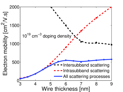
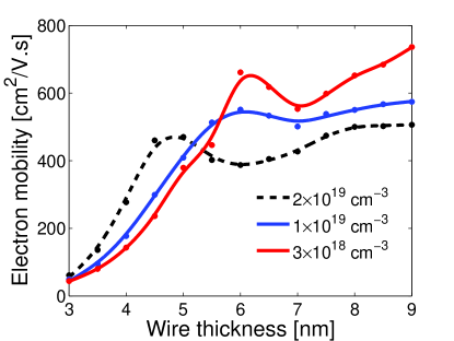
Figure 1b shows the electron mobility as a function of the wire thickness for various wire doping densities. Electron mobility has a peak, followed by a dip, around the wire thickness in which the transition from mostly intrasubband to mostly intersubband scattering happens. The dip in the mobility curve corresponds to the onset of significant intersubband scattering between the lowest two subbands, i.e. the energy difference between the first and second subband bottoms exceeds the polar optical phonon energy. As we can see in Fig. 1b, varying the doping density moves this transition point between mostly inersubband and mostly intrasubband scattering regimes. In thick NWs, similar to bulk, increasing the doping density causes more electron scattering with ionized dopants and the electron mobility decreases. However, for thinner wires the behavior is more complicated and we discuss it in more detail in the next few paragraphs.
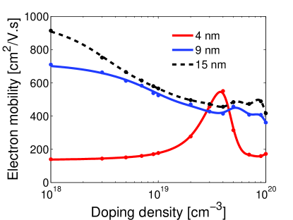
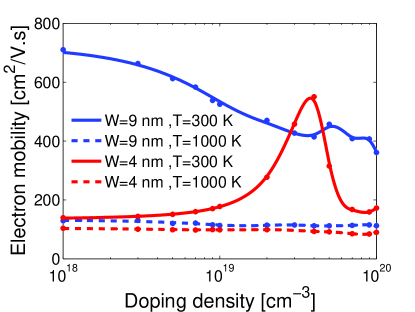
Figure 2 shows the electron mobility dependence on the doping density for various wire thicknesses. These results are in good agreement with the experimental measurements of Huang et al. Huang et al. (2002) for a GaN nanowire FET device of 10 nm thickness. In relatively thick NWs, we observe the expected decrease of the electron mobility with increasing doping density. However, for a NW with a relatively small diameter, the electron mobility shows a more complicated non-monotonic behavior with doping density. Similar behavior has been observed by others in the mobility versus effective field dependence of gated silicon nanostructures, Kotlyar et al. (2004); Ramayya et al. (2007); Jin et al. (2007b) where its origin comes from the interplay of surface roughness and nonpolar intervalley phonon scattering in these confined systems. Jin et al. (2007b) In GaN NWs, strong electron confinement is also key, but POP scattering plays the dominant role instead. The origin of the peak can be readily grasped by relying on the relaxation-time approximation (RTA) expression for the mobility (here are the electron quantum numbers – the subband index, momentum along the NW, and the spin orientation, respectively):
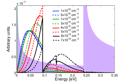
Here, is the Fermi-Dirac distribution function. is the density of states, the lifetime, and is the group velocity along the wire for an electron in the -th subband and with the kinetic energy . We have used the fact that the denominator from the first line of Eq. (II.1), , equals the electron density, which in turn equals the doping density . With increasing doping density, the Fermi level moves up in energy, and the transport window (the energy range where is appreciable) follows. As in NWs, from the integrand in the numerator of Eq. (II.1) we see that the mobility is determined by the product of and within the transport window. Figure 3 shows the integrand from the numerator of Eq. (II.1) divided by the doping density versus energy, for the 4-nm wire and several doping densities ranging cm-3 to cm-3; the area under each curve is therefore proportional to the mobility for that doping density. (The cumulative density of states, , is also presented as a lightly shaded area.) Each integrand curve has a steep drop at roughly 91 meV, corresponding to the relaxation time drop due to the onset of intrasubband POP emission for the first subband, and a small dip at about 145 meV, 91 meV below the second subband bottom, which corresponds to the onset of first-to-second subband intersubband scattering due to POP absorption. For ranging from cm-3 to cm-3, the integrand curves overlap, so the areas under them are nearly the same and the mobility is nearly constant. With a further doping density increase, the transport window moves towards the POP emission threshold; mobility reaches its maximal value when the electronic states with high velocities but still below the POP emission threshold are around the middle of the transport window (doping density about cm-3). As the density increases futher, the transport window moves into the range of energies with strong intrasubband POP emission and the mobility drops.
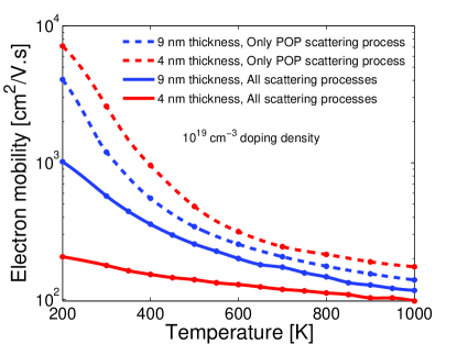
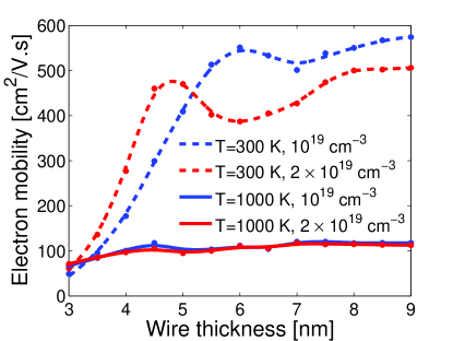
Next, we discuss the effect of a temperature increase on the electron mobility. Figure 4a shows the electron mobility of 4-nm and 9-nm-thick NWs doped to cm-3 with only POP scattering and with all scattering mechanisms included. With increasing temperature, the POP scattering rate increase, following the increasing number of polar optical phonons. For temperatures above 600 K, POP scattering becomes the dominant scattering process and governs the rapid decrease of the electron mobility for the thicker, 9-nm NW. In the thinner 4-nm NWs, the mobility is less sensitive to temperature because the greater strength of SRS with respect to POP scattering in thin wires. Figure 4b shows the electron mobility as a function of the wire thickness at 300 and 1000 K for two doping densities, while Fig. 4c presents mobility versus doping density at 300 and 1000 K for 4-nm and 9-nm NWs. At 1000 K, POP scattering dominates over other mechanisms and the transport window, roughly wide, contains a number of subbands; together, these two effects result in flattening of both the mobility vs. wire thickness (Fig. 4b) and the mobility vs. doping density(Fig. 4c) dependencies.
II.2 The Seebeck Coefficient
The Seebeck coefficient (also known as the thermopower) for bulk GaN has a value of 300 – 400 V/K, depending on the sample and the temperature. Liu and Balandin (2005a); Kaiwa et al. (2007); Sztein et al. (2009) The Seebeck coefficient is a sum of the electronic and the phonon-drag (also known as phononic) contributions. For GaN NWs, our calculation shows that the phonon-drag Seebeck coefficient is about two orders of magnitude smaller than the electronic one at temperatures of interest, so we henceforth neglect the phonon-drag contribution and equate the total and the electronic Seebeck coefficients. In this section, we discuss the effect of the NW thickness, doping density, and temperature on the Seebeck coefficient.
Based on the 1D BTE using the relaxation-time approximation (RTA), we find the Seebeck coefficient () to be
| (7) |
where is the Fermi energy, is the equilibrium Fermi-Dirac distribution, is the relaxation time of electron in subband , and is the energy of the bottom of that subband. Integration over energy is performed from zero to infinity. Note that the Seebeck coefficient is determined by the average excess energy with respect to Fermi energy, , carried by electrons in the vicinity of the Fermi level.
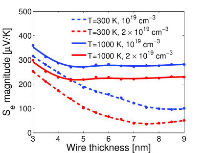
Figure 5a shows as a function of the wire thickness for various doping densities, which are compatible with the experimental results by Sztein et al. Sztein et al. (2009). Decreasing the wire thickness increases the spacing between the subband bottom energies and the Fermi level, which, consequently, increases in an average sense (Fig. 5b). The result is a rise in the Seebeck coefficient. For thicker wires, the Fermi level lies between subband bottoms and the interplay between the contributions from different subbands determines the variation of . As an example of this interplay, we observe a slight increase in the Seebeck coefficient between the 7-nm and 9-nm-thick NWs at the doping density of cm-3.
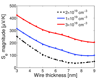
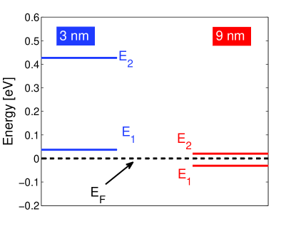
Figure 6a shows the variation of the Seebeck coefficient with doping density for GaN NWs of different thicknesses. Increasing the doping density means more subband bottoms below the Fermi level (Fig. 6b). This effect results in a high Seebeck coefficient for wires with lower doping densities, for which all subbands are above the Fermi level. In contrast, for degenerately doped wires, the Fermi level typically lies between subbands; is determined by an interplay between the position of the different subbands with respect to the Fermi level (Fig. 6b) and the versus doping density curve is almost flat (Fig. 6a).
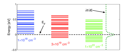
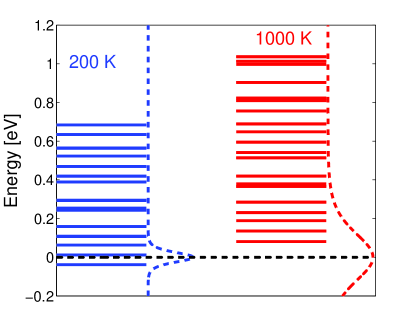
Figure 7a presents the dependence of the Seebeck coefficient on temperature in 4-nm and 9-nm-thick GaN NWs. A major effect of increasing the temperature is broadening of the Fermi-Dirac distribution function. With increasing temperature, but at a fixed doping density and wire thickness, a given subband will be higher in energy with respect to the Fermi level (thereby contributing more favorably to the Seebeck coefficient) and the energy range for electrons active in electrical conduction will widen (Fig. 7a). As seen in Fig. 7b, when the temperature is increased from 200 to 1000 K in a 9 nm thick NW doped to cm-3, the Seebeck coefficient increases by a factor of 3.5.
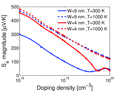
Fig. 8 shows the Seebeck coefficient as a function of doping density (Fig. 8a) and wire thickness (Fig. 8b) at temperatures 300 K and 1000 K. The Seebeck coefficient increases with increasing temperature, as observed in experiment. Chul-Ho Lee and Kim (2009)
III Thermal Transport
In bulk GaN, most experimental measurements of the thermal conductivity have been done at temperature below 400 K.Sichel and Pankove (1977); Jezowski et al. (2003a) Typical experimental values at room temperature are in the range of 130 – 200 W/mK; a good survey of the results prior to 2010 was done by AlShaikhi et al.AlShaikhi et al. (2010) Recent first-principles theoretical calculations by Lindsey et al.Lindsay et al. (2012) give thermal conductivity values for temperatures up to 500 K, with the room-temperature value of about 200 W/mK, in agreement with experiment.Sichel and Pankove (1977); Jezowski et al. (2003a) Based on a theoretical study by Liu and Balandin, Liu and Balandin (2005a) the thermal conductivity of bulk GaN at 1000 K is expected to be about 40 W/mK.
Thermal conductivity in -type NWs comprises two components: phonon (lattice) and electron thermal conductivities. The lattice thermal conductivity of semiconductor nanowires is expected to be very low, based on theoretical work using molecular dynamics,Ponomareva et al. (2007); Papanikolaou (2008); Donadio and Galli (2010, 2009) nonequilibrium Green’s functions in the harmonic approximation,Mingo and Yang (2003); Wang and Wang (2007); Markussen et al. (2009) and the Boltzmann transport equation addressing phonon transport.Chen et al. (2005); Lacroix et al. (2005a, 2006); Mingo and Broido (2004); Mingo et al. (2003) Here, we calculate the lattice thermal conductivity using the phonon ensemble Monte Carlo (EMC) technique, and electronic thermal conductivity using the RTA. While is much lower than in bulk semiconductors, the two can become comparable in highly doped ultrathin NWs, owing to the reduction of that comes from phonon scattering from rough boundaries and the increase in with increasing doping density. The phonon Monte Carlo method used in this work is explained in detail in Lacroix et al.Lacroix et al. (2005b) and Ramayya et al.Ramayya et al. (2012) The Monte Carlo kernel simulates transport of thermal energy carried by acoustic phonons; optical phonons are neglected due to their short lifetime and low group velocity. AlShaikhi et al. (2010); Kamatagi et al. (2007) The important acoustic phonon scattering mechanisms are phonon-phonon (normal and Umklapp), mass difference, and surface roughness (boundary) scattering. AlShaikhi et al. (2010); Kamatagi et al. (2007)
We simulate wires of length greater than the typical mean-free path for bulk, in order to properly describe the diffusive transport regime. If the wires are long enough, a linear temperature profile will be obtained along the wire (in contrast with the steplike ballistic transport signature Ramayya et al. (2012)). Typical wires in our simulations are 200 nm long. There is no volume mesh, only a surface mesh with typically 1 angstrom mesh cell size, which captures roughness scattering. Along the wire axis, the wire is divided into cubic segments of the same length as the wire thickness and width. Each segment is assumed to have a well-defined temperature, which is updated during the simulation, as the phonons enter and leave. Energy that is transferred through each boundary between adjacent segments per unit time is recorded and its value averaged along the wire is used to compute the thermal conductivity based on Fourier’s law.Ramayya et al. (2012)
The normal and Umklapp phonon-phonon scattering rates are calculated using the Holland model. Holland (1963) In contrast to the simpler Klemens-Callaway rates, Callaway (1959) which assume a single-mode linear-dispersion (Debye) approximation, the Holland rates are more complex as they are specifically constructed to capture the flattening of the dispersive transverse acoustic (TA) modes. Holland (1963) For the scattering rate calculation of the TA modes, the zone is split into two regions, such that there is only normal scattering for small wave vectors (roughly up to halfway towards the Brillouin zone edge), while both umpklapp and normal scattering occur for larger wave vectors. Therefore,
| (8a) | |||||
| (8d) | |||||
Relaxation rates for longitudinal acoustic phonons are given by
| (9a) | |||||
| (9b) | |||||
Here, , , , and are the constants shown in Table 2, which are calculated by fitting our simulation results for bulk GaN to experimental results of Sichel et al. Sichel and Pankove (1977) corresponds to the frequency of the transverse branch at point, where is the Brillouin zone boundary. Holland (1963)
| Parameter | Value | Units |
|---|---|---|
| s |
The relaxation rate for mass difference scattering is given by the following expression Klemens (1958)
| (10a) | |||
| where is a sample-dependent constant, given by | |||
| (10b) | |||
Here, is the volume per atom, equal to for the wurtzite crystal. is the average phase velocity given by under the isotropic phonon dispersion approximation. Liu and Balandin (2005b) is the constant which indicates the strength of mass difference scattering. It is defined as , where is the fractional concentration of the atoms type with different mass, , in the lattice. is the average atomic mass, . The parameter due to isotopes for a typical sample is given in Table 3. The parameter due to doping with Si to cm-3 is about , an order of magnitude smaller than for isotopes. Mass difference scattering due to dopants becomes comparable to isotope scattering at about cm-3 doping density; therefore, thermal conductivity has a weak dependence on the doping density. The total relaxation rate is given by .
| Parameter | Value | |
|---|---|---|
| Lattice constant | Å | |
| Lattice constant | Å | |
| L branch phonon group velocity at point | ||
| T branch phonon group velocity at point | ||
| Longitudinal phonon frequency at point | THz | |
| Transverse phonon frequency at point | THz | |
| Transverse phonon dispersion curve fitting parameter | ||
| Longitudinal phonon dispersion curve fitting parameter | ||
| Isotope scattering parameter |
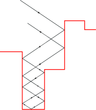
Surface roughness scattering is often modeled using the RTA and a specularity parameter that accounts for diffuse scattering at the surface. Mazumder and Majumdar (2001); Aksamija and Knezevic (2010) Here, we have accounted for SRS more realistically by generating a rough surface with specific rms roughness and correlation length. Ramayya et al. (2012) When a phonon hits the rough surface, it will reflect specularly at the point of impact; this approach is reminiscent of ray-tracing (see, for instance, Refs. Moore et al., 2008; Termentzidis et al., 2013). The phonon can undergo multiple reflections before it returns inside the wire (Fig. 9).
We used a quadratic dispersion relationship, , fitted to the experimental data of Ref. Siegle et al., 1997, for transverse and longitudinal bulk phonons. The quadratic dispersion is quite accurate in wurtzite GaN, as shown, for example, by Ma et al.Ma et al. (2013) is the the sound velocity (i.e. the phonon group velocity at the point). The material parameters are listed in Table 3.
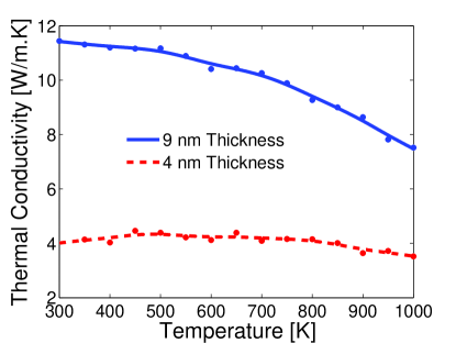
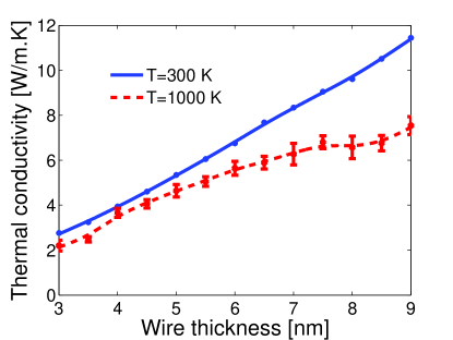
Figure 10 shows thermal conductivity as a function of temperature and wire thickness, for rms roughness of 0.3 nm and a correlation length of 2.5 nm. For these roughness parameters, thermal conductivity in GaN NWs shows a reduction by a factor of 20 with respect to bulk at 300 K, which emphasizes the dominance of SRS in phonon transport over other processes.
The slight waviness in the 1000 K in Fig. 10b is of numerical origin; with increasing temperature the number of real phonons represented by one numerical phonon increases rapidly, which affects accuracy. While the error bars on the 300 K data are too small to be visible, the 1000 K values are of order a few percent (Figure 10b).
IV Figure-of-Merit Calculation
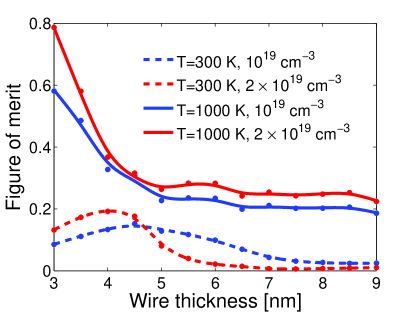
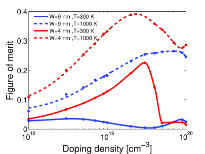
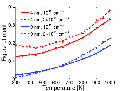
Using the calculated electron mobility, Seebeck coefficient, and lattice thermal conductivity, we compute the TE figure of merit. Figure 11 shows the variation of room-temperature as a function of wire thickness (Fig. 11a), doping density (Fig. 11b), and temperature (Fig. 11c).
The highest room-temperature values in GaN NWs of approximately 0.2 are two-orders-of-magnitude greater than the bulk value of 0.0017 reported by Liu and Balandin, Liu and Balandin (2004, 2005b) an increase that stems both from the thermal conductivity reduction (Fig. 10b) and the Seebeck coefficient increase (Fig. 8b) with decreasing wire thickness. Wires with characteristic cross-sectional features of about 4 nm have the highest values at room temperature; the decrease in with further reduction in thickness comes from the overall detrimental effect of SRS on the electron mobility, which overshadows the beneficial effects of thermal conductivity reduction and increase.
In contrast, at 1000 K, the transport window contains multiple subbands and POP scattering is the dominant scattering mechanism, so the electron mobility is nearly independent of both thickness and doping density. As a result, the of GaN NWs continues to increase with decreasing thickness, and reaches 0.8 in 3-nm-thick GaN NWs for the cm-3 doping density. (For wires thinner than 3 nm, changes in the phonon dispersion and electronic band structure become considerable and atomistic approaches ought to be employed,Neophytou and Kosina (2011b) which may quantitatively change the TE figure of merit.) The of GaN NWs continues to rise with increasing temperature beyond 1000 K, which should ensure efficient energy harvesting with these devices up to high temperatures.
V Conclusion
We presented a comprehensive computational study of the electronic, thermal, and thermoelectric properties of GaN NWs over a broad range of thicknesses, doping densities, and temperatures.
At room temperature, SRS of electrons in thin GaN NWs competes with polar optical phonon scattering, and results in a decrease of the electron mobility with decreasing thickness. Roughness also decreases thermal conductivity in thin wires, which is beneficial in thermoelectric applications. Reduced wire thickness improves the Seebeck coefficient, which is considerably higher in thin wires over in bulk, owing to the combined effects of the 1D subband density-of-states and the increasing subband separation that follows a reduction in the wire cross section. Cumulatively, reducing the wire cross-sectional features down to 4 nm results in the room-temperature increasing, with a maximum of 0.2 obtained for wires of 4-nm thickness doped to cm-3, a two-orders-of-magnitude increase over bulk. Below 4 nm, the room-temperature does not improve with further confinement, as the detrimental surface-roughness-scattering of electrons and the drop in mobility win over the beneficial effects that confinement has on the Seebeck coefficient and thermal conductivity.
At high temperatures, the highest in this study being 1000 K, the electron mobility flattens as a function of thickness, as many subbands start to contribute to transport and POP scattering wins over the temperature-insensitive SRS. The Seebeck coefficient is higher at 1000 K than at 300 K and increases with decreasing wire thickness, although less dramatically than at lower temperatures, while thermal conductivity beneficially decreases with increased confinement. Overall, at 1000 K the thermoelectric figure of merit increases with increasing confinement (i.e. decreasing NW thickness), reaching a value of 0.8 for 3 nm wires.
The of GaN NWs continues to increase with the temperature increasing beyond 1000 K, owing to the negligible minority carrier generation across the large gap, which underscores the suitability of these structures for high-temperature energy-harvesting applications. Extrapolation of the trend would yield at 2000 K for 4-nm-thick NWs. Further improvements in might be achieved by additional alloy scattering of phonons by introducing In, as demonstrated in Ref. Sztein et al., 2013. Combined with nanostructuring, InGaN NWs might prove to be a particularly interesting choice for high-temperature power generation.
VI Acknowledgement
The authors thank Z. Aksamija and T. Kuech for helpful discussions. This work was primarily supported by the NSF grant No. 1121288 (the University of Wisconsin MRSEC on Structured Interfaces, IRG2, funded A.H.D.), with partial support by the AFOSR grant No. FA9550-09-1-0230 (funded E.B.R. and I.K.) and by the NSF grant No. 1201311 (funded L.N.M.).
Appendix A Polar Optical Phonon Scattering
In wurtzite crystals, there is no clear distinction between the longitudinal and transverse optical phonon modes. Based on careful calculations, Yamakawa et al. Yamakawa et al. (2009) have shown that electrons have two orders of magnitude higher scattering rates with the LO-like modes than the TO-like ones, so it is sufficient to consider the LO-like modes alone in electronic transport calculations. Furthermore, there is a profound anisotropy in the bulk electron-phonon scattering rate with respect to the electron momentum (see Yamakawa et al., Ref. Yamakawa et al., 2009). As our wires are assumed to be along the wurtzite c-axis, we consider only LO-like phonons interacting with electrons whose initial and final momenta are along the c-axis. In this case, there is a single relevant phonon energy, whose value of 91.2 meV is taken after Ref. Foutz et al., 1999 and is also given in Table 1.
Here, we show the detailed calculation of the electron-longitudinal polar optical phonon scattering rate. The electric field due to the propagation of a longitudinal optical phonon is given by
| (11) |
where is the polarization vector, () is the phonon creation (annihilation) operator, and is the optical phonon frequency. is the effective interaction parameter given by
| (12) |
Here, and are the high-frequency and low-frequency dielectric permittivities, respectively. From Eq. (11), the perturbing Hamiltonian is equal to
| (13) |
where .
The matrix element for scattering from the initial electronic state to the final state is given by
where plus and minus correspong to emission and absorption of POP, respectively. is the number of optical phonons given by the Bose-Einstein distribution function
| (15) |
We define the function as
| (16) |
and the Eq. (A) yields
According to Fermi’s golden rule, the polar optical phonon scattering rate is given by
| (18) |
By changing the sum to integral we get
Next, we define the overlap integral as
| (20) |
After substituting Eq. (20) into Eq. (18), and converting the integration over wave vector () to the integration over energy (), the final POP scattering rate is written as
| (21) | |||||
where is the optical phonon wave vector along the NW axis. is the final electron kinetic energy, which is given by
| (22) |
Appendix B Piezoelectric Scattering
The creation of a built-in electric field by strain is called the piezoelectric effect, and this field causes piezoelectric scattering of charge carriers. Here, we show a detailed derivation of the piezoelectric scattering rate in GaN NWs. The purturbing Hamiltonian due to the piezoelectric effect is given by
| (23) |
where and are the effective piezoelectric constant and the high-frequency effective dielectric constant, respectively.
The matrix element for scattering from the initial electronic state to the final state is given by
| (24) | |||||
where we used the equipartition approximation for the acoustic phonon population, .
By assuming the linear dispersion relation for acoustic phonons, i.e. , Eq. (24) yields
where is the overlap integral defined in Eq.(16). is called the electromechanical coupling coefficient and is defined as
| (26) |
By perusing an integration procedure similar to the one done for the calculation of POP scattering rate, the piezoelectric scattering rate can be written as
| (27) | |||||
is the acoustic phonon wave vector along the wire axis. The PZ scattering is an elastic process and the finite kinetic energy of electron given by .
References
- Majumdar (2004) A. Majumdar, Science 303, 777 (2004).
- Majumdar (2009) A. Majumdar, Nature Nano. 4, 214 (2009).
- DiSalvo (1999) F. J. DiSalvo, Science 285, 703 (1999).
- Slack (1995) G. A. Slack, “CRC handbook of thermoelectrics,” (CRC Press, Boca Raton, FL, 1995) p. 407–440.
- Shakouri (2006) A. Shakouri, Proc. IEEE 94, 1613 (2006).
- Vineis et al. (2010) C. J. Vineis, A. Shakouri, A. Majumdar, and M. G. Kanatzidis, Adv. Mater. 22, 3970 (2010).
- Hicks and Dresselhaus (1993a) L. D. Hicks and M. Dresselhaus, Phys. Rev. B 47, 16631 (1993a).
- Hicks and Dresselhaus (1993b) L. D. Hicks and M. Dresselhaus, Phys. Rev. B 47, 12727 (1993b).
- Vo et al. (2008) T. T. M. Vo, A. Williamson, V. Lordi, and G. Galli, Nano Lett. 8, 1111 (2008).
- Jeong et al. (2010) C. Jeong, R. Kim, M. Luisier, S. Datta, and M. Lundstrom, J. Appl. Phys. 107, 023707 (2010).
- Kim et al. (2009) R. Kim, S. Datta, and M. S. Lundstrom, J. Appl. Phys. 105, 034506 (2009).
- Kim and Lundstrom (2011) R. Kim and M. S. Lundstrom, J. Appl. Phys. 110, 034511 (2011).
- Neophytou et al. (2011) N. Neophytou, M. Wagner, H. Kosina, and S. Selberherr, J. Electron. Mater. 39, 1902 (2011).
- Neophytou and Kosina (2011a) N. Neophytou and H. Kosina, Phys. Rev. B 83, 245305 (2011a).
- Ramayya et al. (2012) E. B. Ramayya, L. N. Maurer, A. H. Davoody, and I. Knezevic, Phys. Rev. B 86, 115328 (2012).
- Liang et al. (2009) W. Liang, A. I. Hochbaum, M. Fardy, O. Rabin, M. Zhang, and P. Yang, Nano Letters 9, 1689 (2009).
- Ryu et al. (2010) H. J. Ryu, Z. Aksamija, D. M. Paskiewicz, S. A. Scott, M. G. Lagally, I. Knezevic, and M. A. Eriksson, Phys. Rev. Lett. 105, 256601 (2010).
- Venkatasubramanian et al. (2001) R. Venkatasubramanian, E. Siivola, T. Colpitts, and B. O’Quinn, Nature 413, 597 (2001).
- Harman et al. (2002) T. C. Harman, P. J. Taylor, M. P. Walsh, and B. E. LaForge, Science 297, 2229 (2002).
- Snyder and Toberer (2008) G. J. Snyder and E. S. Toberer, Nature Mater. 7, 105 (2008).
- Boukai et al. (2008) A. I. Boukai, Y. Bunimovich, J. Tahir-Kheli, J. Yu, W. A. Goddard III, and J. R. Heath, Nature 451, 168 (2008).
- Hochbaum et al. (2008) A. I. Hochbaum, R. Chen, R. Delgado, W. Liang, E. Garnett, M. Najarian, A. Majumdar, and P. Yang, Nature 451, 163 (2008).
- Lim et al. (2012) J. Lim, K. Hippalgaonkar, S. Andrews, A. Majumdar, and P. Yang, Nano Lett. 12, 2475 (2012).
- Kucukgok et al. (2013) B. Kucukgok, Q. He, A. Carlson, A. G. Melton, I. T. Ferguson, and N. Lu, MRS Proceedings 1490, 161 (2013).
- Sztein et al. (2009) A. Sztein, H. Ohta, J. Sonoda, A. Ramu, J. E. Bowers, S. P. DenBaars, and S. Nakamura, Appl. Phys. Express 2, 111003 (2009).
- Kaiwa et al. (2007) N. Kaiwa, M. Hoshino, T. Yagainuma, R. Izaki, S. Yamaguchi, and A. Yamamoto, 515, 4501 (2007).
- Pantha et al. (2008) B. N. Pantha, R. Dahal, J. Li, H. X. Jiang, and G. Pomrenke, Appl. Phys. Lett. 92, 042112 (2008).
- Yamaguchi et al. (2003) S. Yamaguchi, Y. Iwamura, and A. Yamamoto, Appl. Phys. Lett. 82, 2065 (2003).
- H. Tong and Tansu (2009) V. H. J. H. H. Tong, H. Zhao and N. Tansu, SPIE 7211, 721103 (2009).
- Sztein et al. (2013) A. Sztein, J. Haberstroh, J. E. Bowers, S. P. DenBaars, and S. Nakamura, J. Appl. Phys. 113, 183707 (2013).
- Zou et al. (2002) J. Zou, D. Kotchetkov, A. A. Balandin, D. I. Florescu, and F. H. Pollak, J. Appl. Phys. 92, 2534 (2002).
- Liu and Balandin (2005a) W. Liu and A. A. Balandin, J. Appl. Phys. 97, 123705 (2005a).
- Liu and Balandin (2005b) W. Liu and A. A. Balandin, J. Appl. Phys. 97, 073710 (2005b).
- Chul-Ho Lee and Kim (2009) Y. M. Z. Chul-Ho Lee, Gyu-Chul Yi and P. Kim, Appl. Phys. Lett. 94, 022106 (2009).
- Kuykendall et al. (2003) T. Kuykendall, P. Pauzauskie, S. Lee, Y. Zhang, J. Goldberger, and P. Yang, Nano Lett. 3, 1063 (2003).
- Wang et al. (2006a) G. T. Wang, A. A. Talin, D. J. Werder, J. R. Creighton, E. Lai, R. J. Anderson, and I. Arslan, Nanotechnology 17, 5773 (2006a).
- Wang et al. (2006b) G. T. Wang, A. A. Talin, D. J. Werder, J. R. Creighton, E. Lai, R. J. Anderson, and I. Arslan, Nanotechnology 17, 5773–5780 (2006b).
- Huang et al. (2002) Y. Huang, X. Duan, Y. Cui, and C. M. Lieber, Nano Lett. 2, 101 (2002).
- Simpkins et al. (2007) B. S. Simpkins, P. E. Pehrsson, M. L. Taheri, and R. M. Stroud, J. Appl. Phys. 101, 094305 (2007).
- Motayed et al. (2007) A. Motayed, M. Vaudin, A. V. Davydov, M. He, and S. N. Mohammad, Appl. Phys. Lett. 90, 043104 (2007).
- Talin et al. (2010) A. A. Talin, F. Léonard, A. M. Katzenmeyer, B. S. Swartzentruber, S. T. Picraux, M. E. Toimil-Molares, J. G. Cederberg, X. Wang, and S. D. H. and. A Rishinaramangalum, Semicond. Sci. Technol. 25, 024015 (2010).
- Chang et al. (2006) C.-Y. Chang, G.-C. Chi, W.-M. Wang, L.-C. Chen, K.-H. Chen, F. Ren, and S. Pearton, Journal of Electronic Materials 35, 738 (2006).
- Talin et al. (2009) A. A. Talin, B. S. Swartzentruber, F. Léonard, X. Wang, and S. D. Hersee, J. Vac. Sci. Technol. B 27, 2040 (2009).
- Bloom et al. (1974) S. Bloom, G. Harbeke, E. Meier, and I. B. Ortenburger, physica status solidi (b) 66, 161 (1974).
- Suzuki et al. (1995) M. Suzuki, T. Uenoyama, and A. Yanase, Phys. Rev. B 52, 8132 (1995).
- Albrecht et al. (1998) J. D. Albrecht, R. P. Wang, P. Ruden, M. Farahmand, and K. F. Brennan, J. Appl. Phys. 83, 4777 (1998).
- (47) P. Frajtag, A. Hosalli, J. Samberg, P. Colter, T. Paskova, N. El-Masry, and S. Bedair, Journal of Crystal Growth 352, 203–208.
- Jin et al. (2007a) S. Jin, M. V. Fischetti, and T. W. Tang, 54, 2191 (2007a).
- Ramayya et al. (2008) E. B. Ramayya, D. Vasileska, S. M. Goodnick, and I. Knezevic, J. Appl. Phys. 104, 063711 (2008).
- Ramayya and Knezevic (2010) E. B. Ramayya and I. Knezevic, J. Comput. Electron. 9, 206 (2010).
- Foutz et al. (1999) B. E. Foutz, S. K. O’Leary, M. S. Shur, and L. F. Eastman, J. Appl. Phys. 85, 7727 (1999).
- Prabhakaran et al. (1996) K. Prabhakaran, T. G. Andersson, and K. Nozawa, Appl. Phys. Lett. 69, 3212 (1996).
- Watkins et al. (1999) N. J. Watkins, G. W. Wicks, and Y. Gao, Appl. Phys. Lett. 75, 2602 (1999).
- Lundstrom (2000) M. Lundstrom, Fundamentals of Carrier Transport, 2nd ed. (Cambridge University Press, 2000).
- Yamakawa et al. (2009) S. Yamakawa, R. Akis, N. Faralli, and M. Saraniti, J. Phys.: Condens. Matter 21, 174206 (2009).
- Lagerstedt and Monemar (1979) O. Lagerstedt and B. Monemar, Phys. Rev. B 19, 3064 (1979).
- Kosina and Kaiblinger-Grujina (1998) H. Kosina and G. Kaiblinger-Grujina, Solid-State Electron. 42, 331 (1998).
- Ramayya (2010) E. B. Ramayya, Thermoelectric properties of ultrascaled silicon nanowires, Ph.D. thesis, Department of Electrical and Computer Engineering, University of Wisconsin-Madison (2010).
- Ando et al. (1982) T. Ando, A. B. Fowler, and F. Stern, Rev. Mod. Phys. 54, 437 (1982).
- Kim et al. (2002) J. R. Kim, H. M. So, J. W. Park, J. J. Kim, J. Kim, C. J. Lee, and S. C. Lyu, Appl. Phys. Lett. 80, 3548 (2002).
- Stern et al. (2005) E. Stern, G. Cheng, E. Cimpoiasu, R. Klie, S. Gutherie, J. Klemic, I. Kretzschmar, E. Steinlauf, D. Turner-Evans, E. Broomfield, J. Hyland, R. Koudelka, T. Boone, M. Young, A. Sanders, R. Munder, T. Lee, D. Routenberg, and M. A. Reed, 15, 2941 (2005).
- Cha et al. (2006) H. Y. Cha, H. Wu, M. Chandrashekhar, Y. C. Choi, S. Chae, G. Koley, and M. G. Spencer, 17, 1264 (2006).
- Chin et al. (1994) V. W. L. Chin, T. L. Tansley, and T. Osotchan, Journal of Applied Physics 75 (1994).
- Barker et al. (2005) J. M. Barker, D. K. Ferry, D. D. Koleske, and R. J. Shul, Journal of Applied Physics 97, 063705 (2005).
- Lugli and Ferry (1986) P. Lugli and K. D. Ferry, Phys. Rev. Lett. 56, 1295 (1986).
- Mahan (1998) G. Mahan, “Good thermoelectrics,” (Elsevier Academic Press Inc., San Diego, CA, 1998) pp. 81–157.
- Dogan et al. (2011) P. Dogan, O. Brandt, C. Pfuller, J. Lahnemann, U. Jahn, C. Roder, A. Trampert, L. Geelhaar, and H. Riechert, 11, 4257 (2011).
- Kotlyar et al. (2004) R. Kotlyar, B. Obradovic, P. Matagne, M. Stettler, and M. D. Giles, Appl. Phys. Lett. 84, 5270 (2004).
- Ramayya et al. (2007) E. B. Ramayya, D. Vasileska, S. M. Goodnick, and I. Knezevic, IEEE Trans. Nanotechnol. 6, 113 (2007).
- Jin et al. (2007b) S. Jin, M. V. Fischetti, and T. Tang, J. Appl. Phys. 102, 083715 (2007b).
- Sichel and Pankove (1977) E. K. Sichel and J. I. Pankove, J. Phys. C: Solid State Phys. 38, 330 (1977).
- Jezowski et al. (2003a) A. Jezowski, P. Stachowiak, T. Plackowski, T. Suski, S. Krukowski, I. Grezegory, B. Danilchenko, and T. Paszkiewicz, Planet. Space Sci. 204, 447 (2003a).
- AlShaikhi et al. (2010) A. AlShaikhi, S. Barman, and G. P. Srivastava, Phys. Rev. B 81, 195320 (2010).
- Lindsay et al. (2012) L. Lindsay, D. A. Broido, and T. L. Reinecke, Phys. Rev. Lett. 109, 095901 (2012).
- Ponomareva et al. (2007) I. Ponomareva, D. Srivastava, and M. Menon, Nano Lett. 7, 1155 (2007).
- Papanikolaou (2008) N. Papanikolaou, J. Phys.: Condens. Matter 20, 135201 (2008).
- Donadio and Galli (2010) D. Donadio and G. Galli, Nano Lett. 10, 847 (2010).
- Donadio and Galli (2009) D. Donadio and G. Galli, Phys. Rev. Lett. 102, 195901 (2009).
- Mingo and Yang (2003) N. Mingo and L. Yang, Phys. Rev. B 68, 245406 (2003).
- Wang and Wang (2007) J. Wang and J.-S. Wang, Appl. Phys. Lett. 90, 241908 (2007).
- Markussen et al. (2009) T. Markussen, A.-P. Jauho, and M. Brandbyge, Phys. Rev. B 79, 035415 (2009).
- Chen et al. (2005) Y. Chen, D. Li, J. R. Lukes, and A. Majumdar, J. Heat Transf. 127, 1129 (2005).
- Lacroix et al. (2005a) D. Lacroix, K. Joulain, and D. Lemonnier, Phys. Rev. B 72, 064305 (2005a).
- Lacroix et al. (2006) D. Lacroix, K. Joulain, D. Terris, and D. Lemonnier, Appl. Phys. Lett. 89, 103104 (2006).
- Mingo and Broido (2004) N. Mingo and D. A. Broido, Phys. Rev. Lett. 93, 246106 (2004).
- Mingo et al. (2003) N. Mingo, L. Yang, D. Li, and A. Majumdar, Nano. Lett. 3, 1713 (2003).
- Lacroix et al. (2005b) D. Lacroix, K. Joulain, and D. Lemonnier, Phys. Rev. B 72, 064305 (2005b).
- Kamatagi et al. (2007) M. Kamatagi, N. Sankeshwar, and B. Mulimani, Diamond & Related Materials 16, 98 (2007).
- Holland (1963) M. G. Holland, Phys. Rev. 132, 2461 (1963).
- Callaway (1959) J. Callaway, Phys. Rev. 113, 1046 (1959).
- Klemens (1958) P. G. Klemens, Solid State Physics (Academic, New York, 1958).
- Siegle et al. (1997) H. Siegle, G. Kaczmarczyk, L. Filippidis, A. P. Litvinchuk, A. Hoffmann, and C. Thomsen, Phys. Rev. B 55, 7000 (1997).
- Jezowski et al. (2003b) A. Jezowski, B. A. Danilchenko, M. Bockowski, I. Grzegory, S. Krukowski, T. Suski, and T. Paszkiewicz, Solid State Comm. 128, 69 (2003b).
- Mazumder and Majumdar (2001) S. Mazumder and A. Majumdar, J. Heat Transf. 123, 749 (2001).
- Aksamija and Knezevic (2010) Z. Aksamija and I. Knezevic, Phys. Rev. B 82, 045319 (2010).
- Moore et al. (2008) A. L. Moore, S. K. Saha, R. S. Prasher, and L. Shi, Appl. Phys. Lett. 93, 083112 (2008).
- Termentzidis et al. (2013) K. Termentzidis, T. Barreteau, Y. Ni, S. Merabia, X. Zianni, Y. Chalopin, P. Chantrenne, and S. Volz, Phys. Rev. B 87, 125410 (2013).
- Ma et al. (2013) J. Ma, X. Wang, B. Huang, and X. Luo, Journal of Applied Physics 114, 074311 (2013).
- Liu and Balandin (2004) W. Liu and A. A. Balandin, Appl. Phys. Lett. 85, 5230 (2004).
- Neophytou and Kosina (2011b) N. Neophytou and H. Kosina, Phys. Rev. B 83, 245305 (2011b).