Self-biased Reconfigurable Graphene Stacks
for Terahertz Plasmonics
Abstract
The gate-controllable complex conductivity of graphene offers unprecedented opportunities for reconfigurable plasmonics at terahertz and mid-infrared frequencies. However, the requirement of a gating electrode close to graphene and the single ‘control knob’ that this approach offers limits the practical implementation and performance of these devices. Here we report on graphene stacks composed of two or more graphene monolayers separated by electrically thin dielectrics and present a simple and rigorous theoretical framework for their characterization. In a first implementation, two graphene layers gate each other, thereby behaving as a controllable single equivalent layer but without any additional gating structure. Second, we show that adding an additional gate allows independent control of the complex conductivity of each layer within the stack and provides enhanced control on the stack equivalent complex conductivity. These results are very promising to the development of THz and mid-IR plasmonic devices with enhanced performance and reconfiguration capabilities.
Adaptive MicroNano Wave Systems, École Polytechnique Fédérale de Lausanne (EPFL), 1015 Lausanne, Switzerland.]
Adaptive MicroNano Wave Systems, École Polytechnique Fédérale de Lausanne (EPFL), 1015 Lausanne, Switzerland.
\alsoaffiliation[Department of Electrical & Computer Engineering, University of Texas at Austin, 1 University Station C0803, 78712 Austin, Texas, USA.]
Department of Electrical & Computer Engineering, University of Texas at Austin, 1 University Station C0803, 78712 Austin, Texas, USA.
Nanoelectronics Devices Laboratory, École Polytechnique Fédérale de Lausanne (EPFL), 1015 Lausanne, Switzerland.]
Nanoelectronics Devices Laboratory, École Polytechnique Fédérale de Lausanne (EPFL), 1015 Lausanne, Switzerland.
Laboratory of Electromagnetics and Acoustics (LEMA), École Polytechnique Fédérale de Lausanne, 1015 Lausanne, Switzerland.]
Laboratory of Electromagnetics and Acoustics (LEMA), École Polytechnique Fédérale de Lausanne, 1015 Lausanne, Switzerland.
AntenaLAB, Universitat Polit cnica de Catalunya, C/Jordi Girona 1-3, 08034 Barcelona, Spain]
AntenaLAB, Universitat Polit cnica de Catalunya, C/Jordi Girona 1-3, 08034 Barcelona, Spain
Laboratory of Physics and Complex Matter, École Polytechnique Fédérale de Lausanne, 1015 Lausanne, Switzerland.]
Laboratory of Physics and Complex Matter, École Polytechnique Fédérale de Lausanne, 1015 Lausanne, Switzerland.
Laboratory of Physics and Complex Matter, École Polytechnique Fédérale de Lausanne, 1015 Lausanne, Switzerland.]
Laboratory of Physics and Complex Matter, École Polytechnique Fédérale de Lausanne, 1015 Lausanne, Switzerland.
Nanoelectronics Devices Laboratory, École Polytechnique Fédérale de Lausanne (EPFL), 1015 Lausanne, Switzerland.]
Nanoelectronics Devices Laboratory, École Polytechnique Fédérale de Lausanne (EPFL), 1015 Lausanne, Switzerland.
Adaptive MicroNano Wave Systems, École Polytechnique Fédérale de Lausanne (EPFL), 1015 Lausanne, Switzerland.]
Adaptive MicroNano Wave Systems, École Polytechnique Fédérale de Lausanne (EPFL), 1015 Lausanne, Switzerland.
1 Introduction
The strong graphene-light interaction has led to the rapid development of graphene plasmonics1, 2, which benefit from the unique electrical properties of graphene in the terahertz and mid-infrared frequency bands3. The characterization of single-layer graphene structures has already been performed at microwaves4, 5, 6, 7, terahertz8, 9, 7 and optics3, 10, and some promising applications such as modulators11, 12, 13, 14, 15, 16, plasmonic waveguides17, 18 and Faraday rotators19 have been developed. However, the simple implementation and performance of these devices might be hindered by the presence of a gating electrode located close to graphene and the relatively weak control that this approach offers over the conductivity of graphene11, 20. These limitations can be overcome using graphene stacks, structures composed of two or more isolated graphene layers separated by electrically thin dielectrics, which lead to increased conductivity and may provide novel reconfiguration strategies.
Optical plasmons and quantum transport in such structures have already been studied theoretically21, 22, 23, whereas some experimental studies have focused on the Anderson localization of Dirac electrons in one of the graphene layers at DC due to the screening effect24, 25, 26. Furthermore, the Coulomb drag of massless fermions has been experimentally measured27, while both intra- and inter- layer phenomena in structures surrounded by various dielectrics and their influence in the supported in-phase and out-of-phase plasmons have also been considered28, 29. Potential applications of graphene stacks include modulators12, enhanced metasurfaces30, antennas 31, or plasmonic parallel-plate waveguides18, 32, among many others. Experimentally, graphene stacks have recently been applied to the development of vertical FET transistors33, 34. In addition, the response of unbiased graphene stacks and devices at infrared frequencies has also been investigated20.
In this context, the work herein demonstrates the concept of reconfigurable graphene stacks for THz plasmonics and presents a simple and rigorous theoretical framework for their characterization. Although the graphene monolayers within the stack are not close enough to couple through quantum effects26, 34, their extremely small separation in terms of wavelength allows the stack to behave as a single equivalent layer of increased conductivity. The enhanced tunable capabilities of the proposed structure are experimentally demonstrated in different scenarios, including the mutual gating between the graphene layers and the independent control of each sheet through two different biasing gates. The measurement of the total stack conductivity for various combinations of gate voltages permits not only the extraction of the different parameters that define each of the layers but also the determination of the effective gate capacitance of the surrounding dielectrics. The proposed formulation also allows the design of structures with the desired tunable conductivity behavior. Our results show that reconfigurable graphene stacks boost the available range of complex conductivity values provided by single-layer structures, thus facilitating the easy implementation of THz and mid-infrared plasmonic devices with enhanced reconfiguration capabilities.
2 Results
2.0.1 Operation principle of reconfigurable graphene stacks.
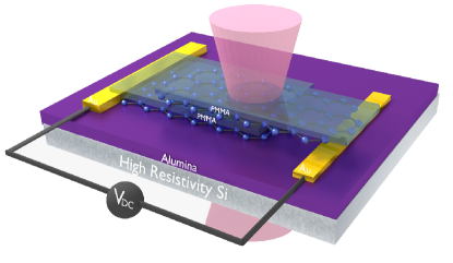
The structure under analysis is shown in Figure 1a, where incident and transmitted beams required for THz time-domain measurements have been artistically rendered. The sample consists of two chemically vapor deposited (CVD) graphene monolayers separated by an electrically thin ( nm) polymethylmethacrylate (PMMA) layer. Metal contacts, added using optical lithography followed by the evaporation of nm of gold, have been included for biasing purposes. The sample is measured in the - THz frequency range using time-domain spectroscopy. The complex conductivity of the graphene stack is then retrieved using a dedicated formulation8, 35, 36. Details regarding the fabrication, measurement, and stack conductivity extraction process are provided in Methods. Because the dielectric separation layer between the graphene layers is extremely thin in terms of wavelengths () 20, an incoming electromagnetic wave observes an stack conductivity
| (1) |
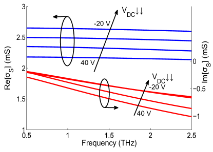
where and are the complex conductivity of the top and bottom graphene layers, respectively. Figure 1c plots the frequency-dependent real and imaginary parts of the extracted conductivity for several DC biasing voltages applied between the graphene layers. In the low terahertz band, the real component of the sample conductivity does not vary with frequency, whereas the imaginary part, which facilitates the propagation of surface plasmons in this frequency band37, increases with frequency following a standard Drude model.
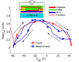
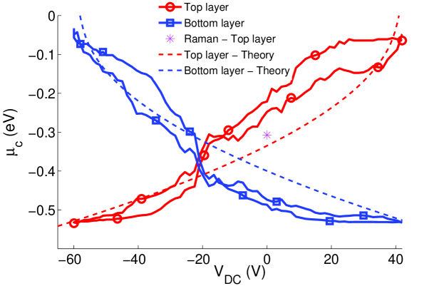
Figure 2 shows the measured reconfiguration capabilities of the fabricated graphene stack at THz in different scenarios. In the first case, depicted in Figure 2a, a gate voltage is applied between the two graphene layers. The results clearly confirm the tunability of and the ability of the stack to self-bias. The extracted chemical potentials corresponding to each graphene sheet, computed using the procedure detailed in Methods combined with the measured stack conductivity and further validated by Raman scattering measurements38, are depicted versus the applied gate voltage in Figure 3. Both graphene layers are -doped, and they present slightly different Fermi levels. This difference can be due to the defects induced in the graphene layers during growth or transfer39 and to the influence of the surrounding dielectrics40, 41, 42. In addition to the different morphology of the surrounding dielectrics, contamination during processing43 and molecules absorbed from ambient air44 play a crucial role. Applying a positive bias between the graphene sheets injects electrons/holes into the top/bottom layers, as illustrated in Supplementary Figure , which in turn increases/decreases their chemical potential (or vice versa in the case of a negative applied bias). Furthermore, the extracted conductivities and chemical potentials exhibit a hysteresis behavior, which arises due to the charges and impurities trapped in the surrounding dielectrics, as occurs in graphene transistors45.
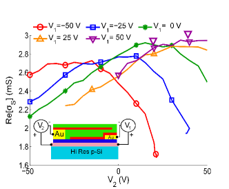
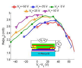
Another interesting possibility for controlling the stack conductivity and boost its tuning range consists of applying voltages and to the bottom and top graphene layers, as illustrated in Figure 2b. For the sake of simplicity, we have implemented this biasing scheme by including an additional polysilicon gate below the lower graphene layer. Alternatively, this configuration might be implemented by stacking a higher number of graphene layers in the same structure. Finally, Figure 2c presents a simple biasing procedure able to control the conductivity of each layer independently. Specifically, applying a fixed voltage between the graphene sheets fixes the chemical potential of the top layer, whereas the carrier density on the bottom layer is tuned by modifying the voltage , as will be theoretically demonstrated below. Note that a voltage V does not exactly simplify this experiment to the one of Figure 2a, due to the weak electrostatic fields that may arise between the bottom graphene sheet and the polysilicon layers in practice (see Methods). The examples illustrated in Figure 2 demonstrate the large potential of graphene stacks for THz plasmonics, as it is possible to control the behavior of the different layers within a unique stack to achieve the complex conductivity required for a desired application.
2.0.2 Static and dynamic characteristics.
The graphene stack is theoretically analyzed in two different but interdependent steps. First, the carrier density on each graphene layer is determined as a function of the applied gate voltages using an electrostatic approach. Second, this information is employed to compute the frequency-dependent conductivity of the stack. In a general case of two graphene sheets biased by different gate voltages and (see inset of Figure 2b and Supplementary Figure ), these carrier densities can be approximated as
| (2) | ||||
| (3) |
where is the electron charge, is the total carrier density in the graphene layer (with p=bottom,top), corresponds to the pre-doping of the sheet, and is the capacitance of the dielectric layer. Once the carrier densities are known, the Fermi level of each graphene layer and the conductivity , which determines the electromagnetic behavior of the whole stack, can be easily computed (see Methods for details). Moreover, Eqs. 2-3 further confirm that it is possible to control the conductivity of each graphene layer independently. Specifically, the carrier density on both layers similarly depends on the difference between the applied voltages (), while the bottom layer additionally depends on the voltage . Consequently, modifying the voltage while keeping constant the difference allows the independent control of each layer’s conductivity.
This simple framework allows a rigorous extraction of the characteristics of the stack from the measured data, including the relaxation time () and the Fermi level () of the graphene layers and the capacitance () of the surrounding dielectrics. This procedure, detailed in Methods, relies on applying different sets of gate voltages to the sample to measure various stack conditions, which in turns allows independent extraction of all of the aforementioned parameters. A system of nonlinear coupled equations is then imposed, relating the measured data to the theoretical characteristics of the stack. In the particular case of the sample shown in Figure 2a, the solution of the system of equations yields ps, ps, eV, and eV, whereas the gate capacitance of the PMMA separation layer is F m. These values are in good agreement with the measured characteristics of a single layer graphene transferred onto a similar dielectric ( ps and eV, as shown in the Supplementary Figures -) and with the gate capacitance obtained using the approximate parallel-plate formula F m. The simulated results, plotted in Figures 2a-3 together with measured data, confirm the accuracy of both the extraction procedure and the proposed model to characterize reconfigurable graphene stacks. The measured hysteresis behavior of the sample conductivity, which is mainly related to the charges trapped in the dielectrics surrounding the graphene layers45, is not considered in the model. In addition, the extracted values permits estimating a modulation speed of kHz for the stack (see Supplementary Note ), similar to the one found in single-layer graphene structures12, 46.
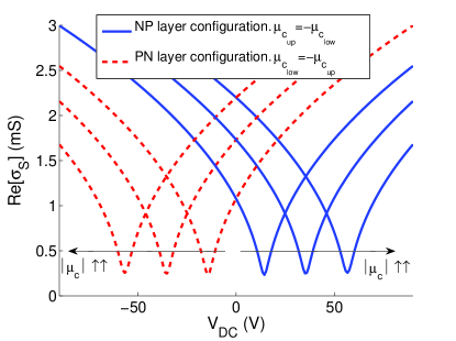
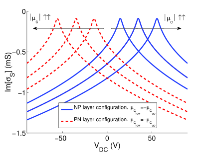
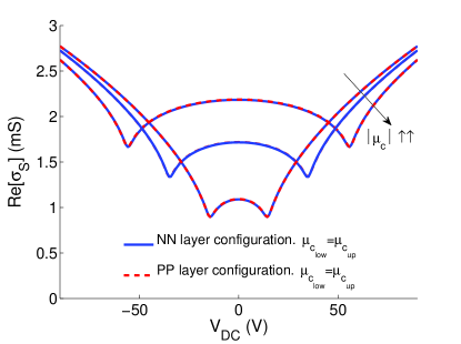
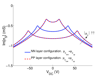
This framework can be further employed to forecast the reconfiguration capabilities of a wide variety of graphene stacks, allowing the design of structures with desired plasmonic properties and tunable behavior. Figure 4 illustrates at THz the real and imaginary conductivity components of a stack composed by two graphene sheets with various Fermi levels versus the gate voltage applied between the layers (see inset of Figure 2a). Let us first consider, for simplicity, a stack where the graphene layers have a different type of doping, i.e., one sheet is -doped and the other is -doped. In this particular case, illustrated in Figsures 4a-4b, the carriers injected by the voltage source alter the carrier density on each layer in a similar way, i.e., simultaneously increasing/decreasing their while keeping their opposite doping nature . As a result, the stack conductivity is approximately twice the conductivity of an individual layer. The behavior of the stack conductivity differs with respect to the previous case when the layers have the same type of doping, i.e., if they are both -doped or -doped. In this case, shown in Figures 4c-4d, the carriers injected by the source modify the carrier density on each graphene sheet in an opposite direction, i.e., increasing of one layer while reducing it on the other layer. Consequently, the stack conductivity presents a symmetrical behavior for positive and negative gate voltages, exhibiting points of minimum conductivity in both cases. The results shown in Figure 4 confirm that in graphene stacks i) the imaginary component of can be double than the one of a single-layer structure, while avoiding the presence of metallic bias, and ii) the tuning range is significantly boosted for similar applied voltages values. In addition, the conductivity of graphene stacks can be controlled further by considering two different gate sources, as shown in the inset of Figure 2b. Similar to the previous case, the tunable behavior of the stack conductivity will strongly depend on the initial level and the type of doping of each graphene layer, leading to a wide variety of scenarios and reconfiguration possibilities (see Supplementary Figures -).
2.0.3 Surface plasmons supported by graphene stacks.
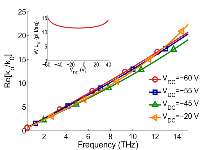
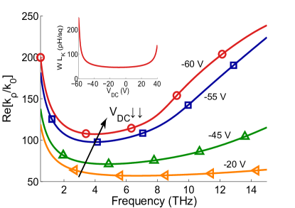
The measured characteristics of the fabricated stack allows to simulate the frequency-dependent properties of the surface plasmons supported by the device. Specifically, the structure supports two different modes47, 32 (see Methods): an even TM and an odd quasi-TEM. The former can easily be seen as a usual TM plasmon propagating along a single-layer graphene sheet with a conductivity equal to the stack conductivity . Figure 5a illustrates the characteristics of this mode, which presents lower field confinement and reduced tunability compared to plasmons in single-layer graphene. This behavior arises due to the increased imaginary component of the stack conductivity, which in turn reduces the kinetic inductance associated to this mode. The later is a perturbation of the TEM mode found in standard parallel-plate waveguides with two perfect electric conductors. Figure 5b confirms that this mode presents remarkable characteristics in terms of field confinement and tunability, clearly outperforming single-layer graphene structures. Note that the high losses associated to CVD graphene48, which prevent the propagation of the supported plasmons along many wavelengths, can be significantly mitigated employing high-quality graphene in the stack49. Supplementary Note includes a comparison of the characteristics of plasmons supported by the stack and a single-layer graphene structure, and further discusses the influence of losses in both cases.
3 Discussion
This theoretical and experimental study of graphene stacks has demonstrated that the available range of complex conductivities in graphene stacks can be significantly boosted by two different approaches i) mutually biasing the graphene sheets without requiring the presence of any metallic bias, and ii) including a third gate source to control the conductivity of each layer independently. The development of graphene stacks for terahertz plasmonic also faces some important challenges from the technological point of view, as it would be desirable to independently control the doping nature of each layer while decreasing the separation distance between the graphene sheets in order to further enhance the reconfiguration possibilities of the stack. Furthermore, inter-layer Coulomb effects28, 29 should be rigorously taken into account in stacks with very small (nm) separation distances between their layers. In addition, it would be also interesting to extend the concept of reconfigurable stacks to an arbitrarily large number of layers. The exotic characteristics of graphene stacks paves the way towards the development of a low-dimensional plasmonic platform with enhanced performance and reconfiguration capabilities. For instance, graphene stacks are the building block of the recently proposed tunable bulk hyperbolic metamaterials50, whereas it has also demonstrated that they are able to boost of the spontaneous emission of emitters51 much further than usual monolayer graphene structures1. In a different context, the large range of imaginary conductivity values provided by the stacks can easily be exploited in planar hyperlenses. Currently, graphene-based hyperlenses52 are based on achieving large contrast of conductivities within the surface by using non-uniform metallic gates located very close to graphene. However, these gates are difficult to fabricate and impair the performance of the lens. This device could easily be implemented by a patterned graphene stack, simultaneously solving the problems related to the limited values of the imaginary conductivity and the presence of the nonuniform metallic gate. Finally, note that the aforementioned features of graphene stacks can also be applied to develop improved devices such as modulators, isolators, sensors, or antennas in the THz and infrared frequency bands.
4 Methods
4.0.1 Fabrication of single-layer and stack graphene structures.
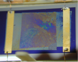
The samples were fabricated using CVD graphene grown on Cu foil and transferred onto the substrate using the standard wet transfer method 53. Supplementary Figure shows the flow of the fabrication process for the double-layer graphene stack. We deposit nm of Al2O3 by atomic layer deposition (ALD) on a an ultrahigh-resistivity () p-type Si wafer. The ALD is performed at C using trimethylaluminum (TMA) and distilled water as the reaction precursors. Prior to the dielectric deposition, the native oxide is removed from the Si wafer with a buffered oxide etch. The metal electrodes are patterned by optical lithography followed by a deposition of nm of chromium, nm of gold and a lift-off process. A graphene sheet is then transferred onto the top of one of the metal contacts. In the double-layer graphene stack, the polymethylmethacrylate (PMMA) layer used as a support polymer during the transfer process is kept on top of the graphene to act as a dielectric between the two graphene sheets. The second graphene monolayer is subsequently transferred onto the top of the other predefined metal contact, thus obtaining the final structure shown in Supplementary Figure d.
The Raman spectra of the graphene employed in our devices is shown in Supplementary Figure . The G and D band points are located at and cm-1 with a full width at half maximum of and cm-1, respectively. The intensity ratio of the D to the G band and of the D to the G band are and . All of these numbers are typical hallmarks of monolayer graphene54. The use of spincoated PMMA as a separation layer between the graphene sheets allows the avoidance of problems associated with standard dielectric deposition techniques such as evaporation, sputtering55 and ALD of oxides, which can induce defects in graphene. This approach is convenient for fabricating graphene stacks, allowing viable biasing schemes without the need of post-processing the graphene. Note that the DC isolation between the two graphene layers of the fabricated stack is not perfect, and some leakage current has been measured. However, it does not hinder the performance of the stack since i) the device does not operate at DC but in the THz band, and ii) graphene field’s effect control is preserved as the DC biasing voltage source is able to provide the required bias voltage, hence the required electrical field, even when some leakage current occurs.
In addition, note that monolayer graphene devices have been annealed in a N2 atmosphere at C during hours 56. The annealing aims removing possible graphene contamination by polymer residues and other impurities 57. However, this process has not been applied to the graphene stack samples because it would remove the PMMA layer which isolates the two graphene sheets.
4.0.2 THz time-domain measurements.
The measurements at terahertz frequencies were performed using a commercial Time Domain Spectrometer (TDTS) (Menlo TERA-K8), which consists of a pulsed femtosecond laser at nm with a pulse repetition rate of MHz and a pulse width around fs, offering with the current experimental setup a signal-to-noise ratio (SNR) of dB up to THz. Two photoconductive antennas based on LT GaAs (Tera-) are used to generate and detect the THz radiation. A set of lenses focuses the THz beam onto the sample under measurement. The total sample area illuminated by the beam is around mm2, thus averaging graphene’s features (see Supplementary Note ). Supplementary Figure presents a schematic view of the experimental setup, with the disposition of the samples and voltage sources.
The gating was applied using a -channel DC voltage source, Agilent NB. Only channels were used for the measurements, and each channel was connected to a different gold contact corresponding to a graphene layer, whereas they both shared a common ground gold contact. For safety reasons and to prevent damaging the graphene stack, the maximum voltage (taking into account both sources) was limited to V. The sample was placed on an X-Y linear stage perpendicular to the THz beam, and everything was placed inside a sealed case purged with to keep a constant atmosphere during the duration of the measurements.
4.0.3 Stack conductivity extraction.
The stack conductivity is extracted from the THz time-domain measurements using standard thin-film characterization techniques58, 36, 8, 35. This approach is valid here thanks to the extreme fineness of the stack in terms of wavelength (). An example of the different set of measured pulses employed for the extraction procedure is shown in Supplementary Figure . To keep the higher possible SNR, we have considered only the first transmitted pulse through the sample. Additional transmitted pulses that arise due to the internal reflections of the THz beam within the layers of the sample are clearly identified thanks to their temporal delay and subsequently removed.
The graphene stack is not free-standing but on top of a thick dielectric structure. Consequently, the influence of the dielectrics must be rigorously removed to extract the actual stack conductivity. This procedure has been performed as follows: i) A pulse is transmitted without the presence of any sample to measure and store the response (including atmosphere and possible impurities) of the sealed cage. ii) A pulse is transmitted through an area of the sample free of graphene, which remains bare. The combination of this measured pulse with the pulse obtained in the previous step allows the extraction of the permittivity, loss tangent and thickness of the dielectrics using standard techniques58, 36. iii) A pulse is transmitted through the graphene stack sample. Combining this measured pulse with the previous information, it is indeed possible to extract the conductivity of the graphene stack rigorously removing the influence of the dielectrics and surrounding atmosphere36, 8, 35.
4.0.4 Graphene stack theory.
The frequency-dependent conductivity of a single graphene layer is modeled using the Kubo formalism59 as
| (4) |
where is the radian frequency, is energy, is a phenomenological electron scattering rate assumed independent of energy, is the electron relaxation time, is temperature, is the charge of an electron, is the reduced Planck’s constant, and is the Fermi-Dirac distribution defined as
| (5) |
being the chemical potential and Boltzmann’s constant. This model results from the long wavelength limit of the bosonic momentum () and takes into account both intraband and interband contributions of the graphene conductivity as well as a finite temperature.
In addition, the carrier density and chemical potential of the graphene layer are related through
| (6) |
where and are the electron and hole densities, respectively, is energy and is the Fermi velocity ( cm s-1 in graphene).
Let us consider the case of two graphene layers closely located within a stack, as depicted in Supplementary Figure . As previously stated, the structure is analyzed first using an electrostatic approach, which determines the carrier density on the graphene layer, and then obtaining the electromagnetic behavior of the stack at THz. Following the superposition principle (see Supplementary Figure b), the carrier density on each layer are computed using Eq. (2)-(3). Note that this electrostatic approach approximates both graphene and polysilicon for infinite perfect conductors in order to compute the carrier density on each layer. Consequently, it cannot predict the presence of weak electrostatic fields that may arise due to i) the different DC conductivities that graphene and polysilicon present in practice, and ii) fringing effects at graphene borders. Combining these expressions with Eq. (6) permits the chemical potential on each graphene layer to be determined. Once these potentials are known, the frequency-dependent complex conductivity of the individual graphene sheets is retrieved using Eq. (4), thus allowing the total graphene stack conductivity to be computed using Eq. (1). Note that in this approach we have neglected i) the influence of the separation layer located between the graphene sheets, which is electrically very small in the THz frequency range, and ii) the possible influence of the quantum capacitance60, which may be significant in the case of high permittivity or extremely thin (nm) dielectrics but is completely negligible here.
Note that the proposed approach approximates graphene’s relaxation time as a constant quantity in each layer, and embeds all variations of graphene conductivity versus the applied bias in the chemical potential7, 61,8. However, rigorous approaches indicate that the relaxation time not only depends on the defects in graphene (), but also on the thermally excited surface polar phonons that may arise at the interface between graphene and the substrate (), and on the frequency-dependent electron-phonon coupling () 62. These values are related through the Matthiessen’s rule 63 by . In addition, graphene relaxation time and chemical potential are not totally independent62. In our particular experiments, the extracted relaxation times are very similar. Since the operation frequency is in the low THz range, well below the graphene optical phonon frequency 62, we expect that electron-phonon phenomenon does not impact the decay mechanism. The similarities among the extracted relaxation times, which correspond to graphene layers surrounded by different substrates, suggests that the graphene/dielectric interface provides a high thus being graphene impurities and nonidealities () the main mechanism limiting the relaxation time, i.e. . Other possible effects such as carrier scattering by ionized impurities 64 and the electron-hole puddle effect 65 might also modify the measured relaxation time.
4.0.5 Extracting the characteristics of each graphene layer.
Let us consider a stack composed of two graphene layers, which are biased by two different gate sources as depicted in Supplementary Figure . The availability of the total stack conductivity for various combinations of gate voltages not only permits the extraction of the different parameters which define each of the layers but also determines the effective gate capacitance of the surrounding dielectrics. Specifically, given a measured stack conductivity obtained by applying a set of gating voltages (, ), Eq. 1 holds. This equation relies on the top and bottom complex conductivities of the layers (), which are computed using the Kubo formula of Eq. 4 and depend on their relaxation time (, ), Fermi levels (, ), gate capacitance of the surrounding media (, ), and the applied gate voltages. Considering a set of measured stack conductivity values, obtained by applying different gate voltages, permits the extension of Eq. 1 into a set of nonlinear coupled equations. The numerical solution of this system of equations determines both the characteristics of each graphene layer within the stack and the gate capacitance of the surrounding media. The solution of these equations may differ slightly as a function of the measured conductivity data employed as an input. These small variations are related to diverse factors, including the hysteresis of the stack conductivity45 or the possible change in the environmental conditions66 (especially humidity) during the measurements. In order to take them into account, the various parameters extracted from all possible combination of gate voltages are finally averaged. Employing a curve fitting approach is not straightforward here as this would involve fitting independent variables, which could lead to non-physical parameter values and complicated post-processing steps.
4.0.6 Surface plasmons supported by a graphene stack.
The dispersion relation of the plasmonic modes supported by a graphene stack can be computed as47
| (7) |
where
| (8) | ||||
| (9) |
, is the direction normal to the structure, and the subscript refers to the top (air), inner (PMMA), and bottom (Al2O3) dielectrics. In addition, denotes the wavenumber of the medium and is the complex wavenumber of the propagating plasmon. Note that we impose Im in order to fulfill Sommerfeld’s radiation condition and we assume that the stack width is much larger than the guided wavelength (i.e., ). The supported even TM and odd quasi-TEM modes described by this dispersion relation can be accurately modeled using per-unit-length equivalent circuits67, 32, 49 (see Supplementary Note ).
5 Author Contributions
J. S. G. and J. P. C. conceived the idea of reconfigurable graphene stacks as well as their application in THz plasmonics. J. S. G. developed the theory and analyzed the measured data. C. M. and A. I. fabricated the devices. L. S. B. and A. M. growth and transferred the graphene layers. S. C. and J. R. performed the THz measurements. J. S. G. wrote the manuscript (with comments from J. P. C and S. C.). J. P. C. led the project.
6 Competing financial interest
The authors declare no competing financial interest.
This work is dedicated to the memory of Professor Julien Perruisseau-Carrier, of the cole Polytechnique F d rale de Lausanne (Switzerland), who passed away unexpectedly while the manuscript was being prepared for publication.
This work was partially supported by the Swiss National Science Foundation (SNSF) under grant , by the European Commission FP projects “Grafol” (Grant. No. ), Marie-Curie IEF “Marconi” (ref. ) and Marie-Curie ITN “NAMASEN”, and by Ministerio de Econom a y Competitividad, Spain, under grant CONSOLIDER CSD2008-00068.
References
- 1 F. H. Koppens, D. E. Chang, and F. J. G. de Abajo, Graphene plasmonics: A platform for strong light-matter interactions, Nano Lett., vol. 11, 3370-3377 (2011).
- 2 A. N. Grigorenko, M. Polini, and K. S. Novoselov, Graphene plasmonics, Nature Photon., vol. 6, 749-758 (2012).
- 3 K. Geim, Graphene: status and prospects, Science, vol. 324, 1530-1532 (2009).
- 4 L. Hao, C. Mattevi, J. Gallop, S. Goniszewski, Y. Xiao, L. Cohen, and N. Klein, Microwave surface impedance measurements on reduced graphene oxide, Nanotechnology, vol. 23, 285706 (2012).
- 5 J. S. G mez-D az, J. Perruisseau-Carrier, P. Sarma, and A. Ionescu, Non-contact characterization of graphene surface impedance at micro and millimeter waves, J. Appl. Phys., vol. 111, 114908 (2012).
- 6 A. Katsounaros, M. T. Cole, H. M. Tuncer, W. I. Milne, and Y. Hao, Near-field characterization of chemical vapor deposition graphene in the microwave regime, Appl. Phys. Lett., vol. 102, 233104 (2013).
- 7 M. Liang and H. Xin, Microwave to terahertz: Characterization of carbon-based nanomaterials, IEEE Microw. Mag., vol. 15, 40-51 (2014).
- 8 L. Ren, Q. Zhang, J. Yao, Z. Sun, R. Kaneko, Z. Yan, S. Nanot, Z. Jin, I. K. amd M. Tonouchi, J. M. Tour, and J. Kono, Terahertz and infrared spectroscopy of gated large-area graphene, Nano Lett., vol. 12, 3711-3715 (2012).
- 9 J. D. Buron, D. H. Petersen, P. Boggild, D. G. Cooke, M. Hilke, J. Sun, E. Whiteway, P. F. Nielsen, O. Hansen, A. Yurgens, and P. U. Jepsen, Graphene conductance uniformity mapping, Nano Lett., vol. 12, 5074-5081 (2012).
- 10 Q. Bao and K. P. Loh, Graphene photonics, plasmonics, and broadband optoelectronic devices, ACS Nano, vol. 6, 3677-3694 (2012).
- 11 L. Ju, B. Geng, J. Horn, C. Girit, M. Martin, Z. Hao, H. A. Bechtel, X. Liang, A. Zettl, Y. R. Shen, and F. Wang, Graphene plasmonics for tunable terahertz metamaterials, Nat. Nanotechnol., vol. 6, 630 (2011).
- 12 B. Sensale-Rodriguez, R. Yan, M. M. Kelly, T. Fang, K. Tahy, W. S. Hwang, D. Jena, L. Liu, and H. G. Xing, Broadband graphene terahertz modulators enabled by intraband transitions, Nat. Commun., vol. 3, 780 (2012).
- 13 B. Sensale-Rodriguez, R. Yan, S. Rafique, M. Zhu, W. Lei, X. Liang, D. Gundlanch, V. Protasenko, M. M. Kelly, D. Jena, L. Liu, and H. G. Xing, Extraordinary control of terahertz beam reflectance in graphene electro-absorption modulators, Nano Lett., vol. 12, 4518-4522 (2012).
- 14 F. Valmorra, G. Scalari, C. Maissenn, W. Fu, C. Scho, J. W. Choi, H. G. Park, and M. Beck, Low-bias active control of terahertz waves by coupling large-area cvd graphene to a terahertz metamaterial, Nano Lett., vol. 13, 3193-3198 (2013).
- 15 R. Degl’Innocenti, D. S. Jessop, Y. D. Shah, J. Sibik, J. A. Zeitler, P. R. Kidambi, S. Hofmann, H. E. Beere, and D. Ritchie, Low-bias terahertz amplitude modulator based on split-ring resonators and graphene, ACS Nano, vol. 8, 2548-2554 (2014).
- 16 S. H. Lee, M. Choi, T. Kim, S. Lee, M. Lui, X. Yin, H. K. Choi, S. S. Lee, C. Choi, S. Choi, X. Zhang, and B. Min, Switching terahertz waves with gate-controlled active graphene metamaterials, Nat. Mater., vol. 11, 936-941, (2012).
- 17 J. T. Kim and S. Y. Choi, Graphene-based plasmonic waveguides for photonic integrated circuits, Opt. Express, vol. 19, 24 557-24 562 (2011).
- 18 J. Christensen, A. Manjavacas, S. Thongrattanasiri, F. H. L. Koppens, and F. J. G. de Abajo, Graphene plasmon waveguiding and hybridization in individual and paired nanoribbons, ACS Nano, vol. 6, 431-440 (2012).
- 19 I. Crassee, J. Levallois, A. L. Walter, M. Ostler, A. Bostwick, E. Rotenberg, T. Seyller, D. van der Marel, and A. B. Kuzmenko, Giant faraday rotation in single and multilayer graphene, Nat. Phys., vol. 7, 48-51 (2010).
- 20 H. Yan, X. Li, B. Chandra, G. Tulevski, Y. Wu, M. Freitag, W. Zhu, P. Avouris, and F. Xia, Tunable infrared plasmonic devices using graphene/insulator stacks, Nat. Nanotechnol., vol. 7, 330 (2012).
- 21 K. Kechedzhi, E. H. Hwang, and S. D. Sarma, Gate-tunable quantum transport in double-layer graphene, Phys. Rev. B, vol. 86, 165442 (2012).
- 22 T. Stauber and G. Gomez-Santos, Plasmons and near field amplification in double-layer graphene, Phys. Rev. B, vol. 85, 075410 (2012).
- 23 J. J. Zhu, S. M. Badalyan, and F. M. Peeters, Plasmonic excitations in coulomb-coupled n-layer graphene structures, Phys. Rev. B, vol. 87, 085401 (2013).
- 24 L. A. Ponomarenko, A. K. Geim, A. A. Zhukov, R. Jalil, S. V. Morozov, K. S. Novoselov, I. V. Grigorieva, E. H. Hill, V. V. Cheianov, V. I. Falko, K. Watanabe, T. Taniguchi, and R. V. Gorbachev, Tunable metal-insulator transition in double-layer graphene heterostructures, Nat. Phys., vol. 7, 958-961 (2011).
- 25 R. V. Gorbachev, A. K. Geim, M. I. Katsnelson, K. S. Novoselov, T. Tudorovskiy, I. V. Grigorieva, A. H. MacDonald, S. V. Morozov, K. Watanabe, T. Taniguchi, and L. A. Ponomarenko, Strong coulomb drag and broken symmetry in double-layer graphene, Nat. Phys., vol. 85, 075410 (2012).
- 26 J. V. Jr, Y. Lee, L. Jing, G. Liu, W. Bao, and C. N. Lau, Quantum transport in double-gated graphene devices, Solid State Commun., vol. 152, 1301-1305 (2012).
- 27 S. Kim, I. Jo, J. Nah, Z. Yao, S. K. Banerjee, and E. Tutuc, Coulomb drag of massless fermions in graphene, Phys. Rev. B, vol. 83, 161401 (2011).
- 28 S. M. Badalyan and F. M. Peeters, Effect of nonhomogenous dielectric background on the plasmon modes in graphene double-layer structures at finite temperatures, Phys. Rev. B, vol. 85, 195444 (2012).
- 29 M. V. Fischetti, Depression of the normal-superfluid transition temperature in gated bilayer graphene, J. Appl. Phys., vol. 115, 163711 (2014).
- 30 A. Fallahi and J. Perruisseau-Carrier, Design of tunable biperiodic graphene metasurfaces, Phys. Rev. B, vol. 86, 195408 (2012).
- 31 M. Tamagnone, J. S. G mez-D az, J. R. Mosig, and J. Perruisseau-Carrier, Reconfigurable thz plasmonic antenna concept using a graphene stack, Appl. Phys. Lett., vol. 101, 214102 (2012).
- 32 D. Correas-Serrano, J. S. Gomez-Diaz, J. Perruisseau-Carrier, and A. Alvarez-Melcon, Spatially dispersive graphene single and parallel plate waveguides: Analysis and circuit models, IEEE Trans. Microw. Theory Tech., vol. 61, pp. 4333-4344 (2013).
- 33 H. Schmidt, . T. Lidtke, P. Barthold, E. McCann, V. I. Falko, and R. J. Haug, Tunable graphene system with two decoupled monolayers, Appl. Phys. Lett., vol. 93, 172108 (2008).
- 34 L. Britnell, R. V. Gorbachev, R. Jalil, B. D. Belle, F. Schedin, A. Mishchenko, T. Georgiou, M. I. Katsnelson, L. Eaves, S. V. Morozov, N. M. R. Peres, J. Leist, A. K. Geim, and K. S. Novoselov, Field-effect tunneling transistor based on vertical graphene heterostructures, Science, vol. 335, 947-950 (2012).
- 35 I. Crassee, M. Orlita, M. Potemski, A. L. Walter, M. Ostler, T. Seyller, I. Gaponenko, J. Chen, and A. B. Kuzmenko, Intrinsic terahertz plasmons and magnetoplasmons in large scale monolayer graphene, Nano Lett., vol. 12, 2470-2474 (2012).
- 36 M. Naftaly and R. E. Miles, Terahertz time-domain spectroscopy for material characterization, Proc. IEEE, vol. 95, 1658-1665 (2007).
- 37 G. W. Hanson, Dyadic green’s functions and guided surface waves for a surface conductivity of graphene, J. Appl. Phys., vol. 103, 06430 (2008).
- 38 A. Das, S. Pisiana, B. Chakraborty, S. Piscanec, K. Saja, U. V. Waghmare, K. S. Novoselov, H. R. Krishnamurthy, A. K. Geim, A. C. Ferrari, and A. K. Sood, Monitoring dopants by raman scattering in a electrochemically top-gated graphene transistor, Nat. Nanotechnol., vol. 3, 210-215 (2008).
- 39 F. Banhart, J. Kotakoski, and A. V. Krasheninnikov, Structural defects in graphene, ACS Nano, vol. 5, 26-41 (2011).
- 40 C. Jang, S. Adam, J. H. Chen, E. D. William, S. D. Sarma, and M. S. Fuhrer, Tuning the effective fine structure constant in graphene: opposing effects of dielectric screening on short- and long- range potential scattering, Phys. Rev. Lett., vol. 101, 146805 (2008).
- 41 A. Konar, T. Fang, and D. Jena, Effect of high-k gate dielectrics on charge transport in graphene-based field effect transistors, Phys. Rev. Lett., vol 82, 11545 (2011).
- 42 P. Sharma, J. Perruisseau-Carrier, C. Moldovan, and A. M. Ionescu, Electromagnetic performance of rf nems graphene capacitive switches, IEEE Trans. Nanotech., vol. 13, 70-79 (2014).
- 43 M. Ishigami, J. H. Chen, W. G. Cullen, M. S. Fuhrer, and E. D. Williams, Atomic structure of graphene on SiO2, Nano Lett., vol. 7, 1643 (2007).
- 44 F. Schedin, A. K. Geim, S. V. Morozov, E. W. Hill, P. Blake, M. I. Katsnelson, and K. S. Novoselov, Detection of individual gas molecules adsorbed on graphene, Nat. Mater., vol. 6, 652-655 (2007).
- 45 H. Wang, Y. Wu, C. Cong, J. Shang, and T. Yu, Hysteresis of electronic transport in graphene transistors, ACS Nano, vol. 4, 7221-7228 (2010).
- 46 B. Sensale-Rodriguez, S. Rafique, R. Yan, M. Zhu, V. Protasenko, D. Jena, L. Liu, and H. G. Xing, Terahertz imaging employing graphene modulator arrays, Opt. Express, vol. 21, 2324-2330 (2013).
- 47 G. W. Hanson, Quasi-transverse electromagnetic modes supported by a graphene parallel-plate waveguide, J. Appl. Phys., vol. 104, 084314 (2008).
- 48 H. S. Song, S. L. Li, H. Miyazaki, S. Sato, K. Hayashi, A. Yamada, N. Yokoyama, and K. Tsukagoshi, Origin of the relatively low transport mobility of graphene grown through chemical vapor deposition, Sci. Rep., vol. 2, 337 (2012).
- 49 H. Yoon, C. Forsythe, L. Wang, N. Tombros, K. Watanabe, T. Taniguchi, J. Hone, P. Kim, and D. Ham, Measurement of collective dynamical mass of dirac fermions in graphene, Nat. Nanotechnol., vol. 9, 594-599 (2014).
- 50 M. A. K. Othman, C. Guclu, and F. Capolino, Graphene-based tunable hyperbolic metamaterials and enhanced near-field absorption, Opt. Express, vol. 21, 7614-7632 (2013).
- 51 L. Zhang, X. Fu, M. Zhang, and J. Yang, Spontaneous emission in paired graphene plasmonic waveguide structures, Opt. Express, vol. 21, 7897 (2013).
- 52 E. Forati, G. Hanson, A. Yakovlev, and A. Alù, Planar hyperlens based on a modulated graphene monolayer, Phys. Rev. B, vol. 89, 081410 (2014).
- 53 A. Reina, H. Son, L. Jiao, B. Fan, M. S. Dresselhaus, Z. Liu, and J. Kong, Transferring and identification of single- and few-layer graphene on arbitrary substrates, J. Phys. Chem. C, vol. 112, 17 741-17 744 (2008).
- 54 A. C. Ferrari, J. C. Meyer, V. Scardaci, C. Casiraghi, M. Lazzeri, F. Mauri, S. Piscanec, D. Jiang, K. S. Novoselov, S. Roth, and A. K. Geim, Raman spectrum of graphene and graphene layers, Phys. Rev. Lett., vol. 97, 187401 (2006).
- 55 M. C. Lemme, T. J. Echtermeyer, M. Baus, and H. Kurz, A graphene field-effect device,IEEE Electron Device Lett., vol. 28, 282-284 (2007).
- 56 W. Xueshen, L. Jinjin, Z. Qing, Z. Yuan, and Z. Mengke, Thermal annealing of exfoliated graphene, J. Nanomater, vol. 2013, 101765 (2013).
- 57 Y. Lin, C. C. Lu, C. H. Yeh, C. Jin, K. Suenaga, and P. W. Chiu, Graphene annealing: How clean can it be?, Nano Lett., vol. 12, 414-419 (2012).
- 58 M. Nuss and J. Orenstein, “Terahertz time-domain spectroscopy,” in Millimeter and Submillimeter Wave Spectroscopy of Solids, ser. Topics in Applied Physics, vol. 74, 7-50 (1998)
- 59 V. P. Gusynin, S. G. Sharapov, and J. B. Carbotte, On the universal ac optical background in graphene, New J. Physics, vol. 11, 095013 (2009).
- 60 Z. Chen and J. Appenzeller, Mobility extraction and quantum capacitance impact in high performance graphene field-effect transistor devices, in IEEE International Electron Devices Meeting (IEDM), San Francisco, USA, 15-17 (2008).
- 61 W. Liu, R. Valdes-Aguilar, Y. Hao, R. S. Ruoff, and N. P. Armitage, Broadband microwave and time-domain terahertz spectroscopy of chemical vapor deposition grown graphene, J. Appl. Phys., vol. 110, 083510 (2011).
- 62 M. Jablan, H. Buljan, and M. Soljacic, Plasmonics in graphene at infrared frequencies, Phys. Rev. B, vol. 80, 245435 (2009).
- 63 W. Zhu, V. Perebeinos, M. Freitag, and P. Avouris, Carrier scattering, mobilities, and electrostatic potential in monolayer, bilayer, and trilayer graphene, Phys. Rev. B, vol. 80, 235402 (2009).
- 64 S. Adam, E. H. Hwang, V. M. Galitski, and S. D. Sarma, A self-consistent theory for graphene transport, Proc. Nat. Acad. Sci, vol. 10, 392-397 (2007)
- 65 J. H. Chen, C. Jang, S. Adam, M. S. Fuhrer, E. D. Williams, and M. Ishigami, Charged-impurity scattering in graphene, Nat. Phys., vol. 4, 377-381 (2008).
- 66 J. Moser, A. Verdaguer, D. Jimenez, A. Barreiro, and A. Bachtold, The environment of graphene probed by electrostatic force microscopy, Appl. Phys. Lett., vol. 92, 123507 (2008)
- 67 F. Rana, Graphene terahertz plasmon oscillators, IEEE Trans. Nanotech., vol. 7, 91-99 (2008).
7 Figures