Termination-dependent Surface In-gap States in a Mixed-valent Topological Insulator: SmB6
Abstract
We have investigated the surface states of a potential mixed-valent topological insulator SmB6 based on the first principles density functional theory slab band structure analysis. We have found that metallic surface states are formed in the bulk band gap region, providing evidence for the topological insulating nature of SmB6. The obtained surface in-gap states are quite different from those in existing reports in that they are formed differently depending on the Sm or B6 surface termination, and are composed of mainly Sm state indicating the essentiality of including electrons in describing the surface states. We have obtained the spin chiral structures of the Fermi surfaces, which are also in accordance with the topological insulating nature of SmB6.
pacs:
71.20.-b, 71.20.Eh, 71.18.+y, 71.15.NcThe low-temperature residual conductivity in a typical Kondo insulator SmB6 has been a long-standing unresolved problem. In this respect, recent reports on the topologically protected metallic surface states in SmB6 have attracted great attentions. transport_Fisk ; Shi-ARPES ; Hasan-ARPES ; MinChulHee-ARPES ; Denlinger-ARPES ; Wang-STS ; Chen-AMR ; Coleman1 ; Coleman2 ; Takimoto ; Gutzwiller Angle-resolved photoemission spectroscopy (ARPES) can provide direct evidence for topological insulators via observation of the Fermi surfaces arising from the surface in-gap states. Indeed, Fermi surfaces were observed in several ARPES studies at and points of the surface Brillouin zone (BZ), Shi-ARPES ; Hasan-ARPES ; Golden-ARPES ; Kimura-ARPES supporting the topological Kondo insulating nature of SmB6. Unfortunately, however, no explicit Dirac cone feature has been observed. Hence, some groups interpreted the metallic states observed in ARPES not as topological surface states but as bulk-shifted or normal (trivial) surface states. Pol_driven_SS ; Golden-ARPES Especially, the origin of the metallic bands at and is controversial as to whether they come from bulk or surface states. Shi-ARPES ; Hasan-ARPES ; Denlinger-ARPES ; Golden-ARPES ; Kimura-ARPES Above all, the spin polarizations of the metallic surface bands has not been unveiled yet. MinChulHee-ARPES ; Imada-ARPES
Among many difficulties, the surface instability in SmB6 prevents revealing the topological nature. Since the chemical bonding between Sm and B6 ions is not weak, the natural cleavage plane in SmB6 is not well defined. The pristine Sm- and B6-terminated surfaces, which are electrically polar and highly reactive, are likely to undergo disordered reconstructions or contaminations. Due to this reason, the topological nature arising from the intrinsic surface states is not easily confirmed experimentally. Another difficulty with SmB6 is the strong correlation effect of electrons. The highly renormalized bands require extremely high-resolution ARPES experiment. Nevertheless, the topological invariance of SmB6, which has been confirmed by a couple of theoretical studies,Takimoto ; Gutzwiller arouse great curiosity about the characteristics of the metallic surface states in SmB6.Robustness
There have been a few surface band calculations which tried to identify the topological properties of SmB6. TakimotoTakimoto and Lu et al.Gutzwiller performed the (001) surface model calculations based on the density functional theory (DFT) and the DFT+Gutzwiller bulk band structures, respectively. Both of them obtained the metallic surface states in the bulk gap region, which produce three Dirac cones and the corresponding Fermi surfaces at and . This feature suggests the nontrivial topological nature of SmB6. But they considered neither the surface termination dependence nor the surface relaxation effect. Zhu et al.Pol_driven_SS performed the DFT slab calculations, and also obtained the surface states in the vicinity of the Fermi level (EF). But their surface states come from the polarity-driven boron dangling bond, and so they claimed that the metallic surface states in SmB6 are not the topologically protected surface states but the normal surface states. In their surface slab calculations, however, they considered the Sm electrons as core. Since the - hybridization is essential to develop the insulating state in bulk SmB6, it is likely that their surface band structures are not relevant to -electron system of SmB6.
In this letter, we have investigated systematically the (001) surface states of a potential mixed-valent topological insulator SmB6, using the first principles DFT calculations on the slabs with different surface terminations. We have first compared the bulk band structures obtained by the DFT with those obtained by the dynamical mean-field theory (DMFT), whereby we have shown that the DFT is useful to investigate the low energy band structure of strongly correlated mixed-valent insulator SmB6. Then, we have performed the DFT surface band structure calculations, and found that the surface bands and the corresponding Fermi surfaces are quite different from those in literature.Takimoto ; Gutzwiller ; Pol_driven_SS The gapless surface states are formed differently for the Sm- and B6-terminated surfaces. Moreover, additional surface states appear around for the Sm-terminated case. We thus argue the importances of considering the Sm electrons and the termination dependence in describing the surface states of SmB6. Further, we have carefully examined the spin chiralities of the Fermi surfaces to corroborate the topological insulating nature of SmB6.
We have investigated the electronic structures of bulk SmB6 using both the DFT and the DMFT incorporating the spin-orbit coupling (SOC). To describe the surface states, two slab geometries were used ; Sm- and B6-terminated slabs. For the DFT, we employed both WIEN2kWIEN2k and VASP code.VASP , while, for the DFT+DMFT, we used the scheme implemented based on WIEN2k.DMFT To scrutinize the spin chirality of each Fermi surface originating from the surface states, the spin-noncollinear calculations were performed. Further details are provided in the supplement.Supp
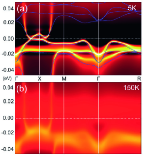
DMFT band structures in Fig. 1 demonstrate the temperature (T) dependent - hybridization behavior. At high T=150K in Fig. 1(b), Sm electrons do not form coherent bands, and so the metallic Sm band crossing EF is clearly visible around X, reflecting little hybridization with incoherent -bands. Upon cooling, the electrons form the coherent bands that become strongly hybridized with the band so as to display a gap feature, even though the gap size is almost zero in the DMFT result of Fig. 1(a) (T=5 K).
In Fig. 1(a), the DMFT bands are overlaid with DFT bands that are rescaled down in energy by 1/10 (thin dotted blue). It is seen that the DMFT and DFT band structures near EF are essentially the same as each other. This feature suggests that the strong correlation effect of electrons can be captured to some extent just by renormalizing DFT bands. The gap feature persists in the renormalized DFT band structure with a reduced size of meV with respect to the original gap size of meV. Of course, the renormalized DFT cannot simulate the Sm bands that are to be shifted up by the strong correlation of Sm electrons. So the position of Sm bands in the DFT is located much closer to EF than in the DMFT. In fact, the present authors have previously analyzed the influence of the low-lying Sm bands on the states near EF.CJ This effect is discussed more in the supplement.Supp
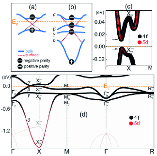
In typical topological insulators such as Bi2Se3 or Bi2Te3, the parity inversion occurs at a high symmetry point between two bulk bands having different parities, and the topologically protected surface states emerge in the gap region, as shown in Fig. 2(a). SmB6, however, shows peculiar parity inversion feature. As discussed in Fig. 1, the occurrence of the gap in SmB6 is initiated by the - hybridization near X, but the band gap is seen to be realized between two -bands, as shown Fig. 2(b)-(d). Namely, there are two more bands, and , having the same negative parity (X) in-between parity inverted bands of (X) and (X). Therefore, some part of the surface in-gap states including the Dirac point would be buried in the bulk and bands, as in Fig. 2(b). This feature in SmB6 is different from usual topological insulators, in which the Dirac cone features are clearly observed in the gap region. This is an important difference, making SmB6 more complicated than other conventional topological insulators.
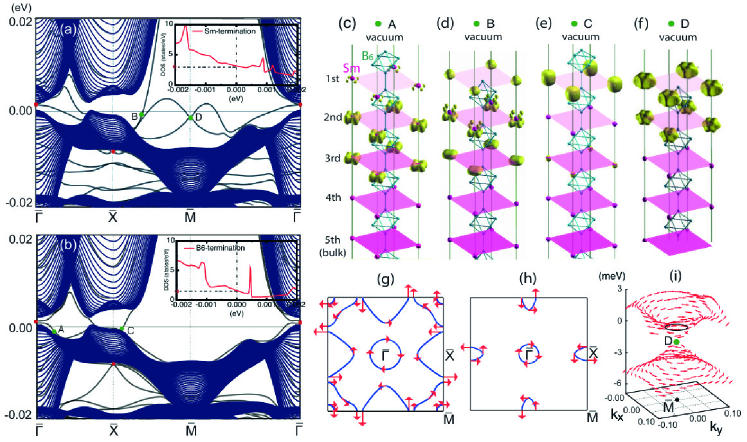
In order to probe into the surface states of SmB6, we have performed the DFT slab calculations for both Sm- and B6- terminated (001) surfaces, including Sm electrons as valence electrons. Figure 3(a) and (b) show the surface states of Sm- and B6- terminated SmB6 slabs, respectively. In both cases, there appear metallic surface states in the bulk gap region, which are seen to merge into bulk bands projected to the surface BZ. The surface in-gap states here are composed of mainly Sm state (the weight of -component is more than 90%). This result is quite contrary to the previous DFT surface band calculation,Pol_driven_SS in which the surface states near EF came mostly from B- dangling bond state. This discrepancy arises from that Sm electrons were not taken into account as valence electrons in Ref. Pol_driven_SS . Without Sm- electrons, we also obtained the B- surface states that cross EF.2.0SS However, in this case, there are many other metallic bands near EF besides the B- surface bands due to the lack of hybridization with electrons, which is certainly in disagreement with ARPES data. Note that the B- surface states do not satisfy the criterion of the topological insulator, whereas the present surface states including Sm electrons do on both terminations. Thus the inclusion of electrons as valence state changes the situation near EF dramatically.
At a glance, the surface states in Fig. 3(b) for the B6-terminated case look analogous to those obtained by the tight-binding (TB) surface model calculation based on the LDA + Gutzwiller bulk band result.Gutzwiller However, there are interesting differences. First, in the TB result, the gapless surface states, especially at , seem to be generated from the band manifesting the Dirac points in the gap region, while, in the present rescaled DFT, the Dirac point is seen to be just buried in the band . This is not a minor distinction. Since the parities of bulk band and are negative, the absence of both bands does not change the topological order. So the gapless surface states are not formed via the bulk band and , but formed just passing through both bands.Soo_yong Interestingly, a similar feature of buried Dirac point in the bulk bands is also seen in PuB6, which was reported to be a correlated topological insulator.PuB6
Secondly, Sm-termination in Fig. 3(a) shows additional surface in-gap states centered at , which have never been recognized theoretically. The existence of these metallic surface states does not violate the EF crossing criterion of Z2 topological characterization. The different surface states depending on the terminations are quite natural even in conventional topological insulators.termination_dep It is, however, rarely reported in real materials that additional metallic surface states emerge with different dispersions at another high symmetry point. Metallic surface states centered at have not been reported experimentally either. One reason why -centered surface states have not been detected might be due to a fact that the size of well-ordered Sm-terminated surface known until now is not over a few nanometers.Harvard-STS ; DRESDEN-STS The beam spot size of state-of-art ARPES may not be enough to capture the physics of such small ordered Sm-terminated surface.
According to recent STM/STSDRESDEN-STS data on the non-reconstructed ordered Sm- and B6-surface terminated SmB6, the differential conductance of the former is about 30 larger than that of the latter at T=4.6 K. This implies that there are additional conducting channels at the Sm-terminated surface, suggesting the higher density of states (DOS) near EF. Indeed, insets of Fig. 3(a) and(b) shows the surface DOSs, which shows about 50 larger DOS at EF in the case of Sm-terminated surface, which matches well with the STS/STM result. So the metallic surface states at can explain the larger differential conductance on the Sm-terminated surface.
Figure 3(c)-(f) show the charge densities of surface wave functions at specific points. It is shown that the charge densities of the surface states originate indeed from the surface atoms, mainly from Sm atoms, of both terminated slabs. It is worthwhile to note in Fig. 3(c) that the surface state near (A) is quite discernible from other surface states near and (B, C, D), in that the dominant charge density at A is slightly away from the topmost layer and locates rather close to the bulk side. This is also the case for the surface state at for the Sm-termination. This feature suggests that the surface state at could be robuster than other surface states against any changes at the surface.
Figure 3(g) and (h) present the Fermi surfaces (FSs) of surface states together with spin chiral structures. It is seen that both terminations have FSs at and with the same helical spin polarization, even though the FSs of the B6-termination are smaller than those of the Sm-termination. In both cases, FSs at and are hole and electron FSs, respectively. Also, due to the surface states of the Sm-termination around , there appear additional FSs of flower shape centered at for the Sm-termination case in Fig. 3(g). These FSs also have helical spin polarizations. The spin texture of the surface state at is more specifically shown in Fig. 3(i), which reveals the opposite helicities above and below the Dirac point D. Therefore, not only previously reported surface states at and but also that at has Dirac cone-like spin texture. This feature corroborates the topological nature of the surface states in SmB6. One thing to be pointed out is that the -centered FSs could be fragile with respect to any environmental perturbations on the surface. It is because, even without the -centered FSs, the criterion for nontrivial topology, i.e. an odd number of EF crossings, is still valid.Supp
In conclusion, we have investigated the surface in-gap states of SmB6 based on the first principles DFT slab band structure analysis. We have found that (i) the surface states and corresponding FSs emerge at around and , (ii) there appear additional surface states centered at for the Sm-termination case, and (iii) more importantly, the present surface states are quite different from those of existing surface band calculations, such as the TB slab calculation and the DFT calculation without considering Sm 4 electrons. We have also determined the spin helicities of Fermi surfaces, which are consistent with the topological Kondo insulating nature of SmB6. For the clear confirmation, spin-resolved ARPES on the ordered surface is strongly recommended.
Acknowledgments We would like to thank Jinwoong Kim and J. H. Shim for helpful discussions. This work was supported by the NRF (Grant No.2009-0079947, No. 2011-0025237), the POSTECH BSRI Grant, and the KISTI supercomputing center (Grant No. KSC-2012-C3-055). J.S.K. acknowledges support by the NRF (Grant No. 2011-0022444). J.D.D. is supported by the U.S. DOE (Grant No. DE-AC02-05CH11231).
References
- (1) S. Wolgast, Ç. Kurdak, K. Sun, J. W. Allen, D.-J. Kim, and Z. Fisk, Phys. Rev. B 88 180405(R) (2013).
- (2) N. Xu, X. Shi, P. K. Biswas, C. E. Matt, R. S. Dhaka, Y. Huang, N. C. Plumb, M. Radovíc, J. H. Dil, E. Pomjakushina, K. Conder, A. Amato, Z. Salman, D.McK. Paul, J. Mesot, H. Ding, and M. Shi, Phys. Rev. B 88, 121102(R) (2013)
- (3) M. Neupane, N. Alidoust, S.-Y. Xu, T. Kondo, D.-J. Kim, Chang Liu, I. Belopolski, T.-R. Chang, H.-T. Jeng, T. Durakiewicz, L. Balicas, H. Lin, A. Bansil, S. Shin, Z. Fisk, and M. Z. Hasan, Nat. Commun. 4, 2991 (2013)
- (4) C.-H. Min, P. Lutz, S. Fiedler, B. Y. Kang, B. K. Cho, H. -D. Kim, H. Bentmann, and F. Reinert, arXiv:1312.1834 (2013).
- (5) J. D. Denlinger, J. W. Allen, J. -S. Kang, K. Sun, J. -W. Kim, J. H. Shim, B. I. Min, D.-J. Kim, and Z. Fisk, arXiv:1312.6637 (2013).
- (6) Wei Ruan, Cun Ye, Minghua Guo, Fei Chen, Xianhui Chen, Guang-Ming Zhang, and Yayu Wang, Phys. Rev. Lett. 112, 136401 (2014).
- (7) F. Chen, C. Shang, A. F. Wang, X. G. Luo, T. Wu, and X. H. Chen, arXiv:1309.2378 (2013)
- (8) M. Dzero, K. Sun, V. Galitski, and P. Coleman, Phys. Rev. Lett. 104, 106408 (2010).
- (9) T. Takimoto, J. Phys. Soc. Jpn. 80, 123710 (2011).
- (10) M. Dzero, K. Sun, P. Coleman, and V. Galitski, Phys. Rev. B 85, 045130 (2012).
- (11) F. Lu, J. Z. Zhao, H. Weng, Z. Fang, and X. Dai, Phys. Rev. Lett 110, 096401 (2013).
- (12) H. Miyazaki, T. Hajiri, T. Ito, S. Kunii, and S.-I. Kimura, Phys. Rev. B 86, 075105 (2012)
- (13) E. Frantzeskakis, N. de Jong, B. Zwartsenberg, Y. K. Huang, Y. Pan, X. Zhang, J. X. Zhang, F. X. Zhang, L. H. Bao, O. Tegus, A. Varykhalov, A. de Visser, and M. S. Golden, Phys. Rev. X 3, 041024 (2013).
- (14) Z.-H. Zhu, A. Nicolaou, G. Levy, N. P. Butch, P. Syers, X. F. Wang, J. Paglione, G. A. Sawatzky, I. S. Elfimov, and A. Damascelli, Phys. Rev. Lett. 111, 216402 (2013).
- (15) S. Suga, K. Sakamoto, T. Okuda, K. Miyamoto, K. Kuroda, A. Sekiyama, J. Yamaguchi, H. Fujiwara, A. Irizawa, T. Ito, S. Kimura, T. Balashov, W. Wulfhekel, S. Yeo, F. Iga and S. Imada, J. Phys. Soc. Jpn. 83, 014705 (2014).
- (16) Z.K. Liu, Y.L. Chen, J.G. Analytis, S.K. Mo, D.H. Lu, R.G. Moore, I.R. Fisher, Z. Hussain, Z.X. Shen, Physica E 44, 891 (2012).
- (17) B. Blaha, K. Schwarz, G. K. H. Madsen, D. Kvasnicka, and J. Luitz, WIEN2k, An Augmented Plane Wave Plus Local Orbitals Program for Calculating Crystal Properties (Vienna University of Technology, Austria, 2001).
- (18) VASP code, http://cms.mpi.univie.ac.at/vasp
- (19) K. Haule, C.-H. Yee, and K. Kim, Phys. Rev. B 81, 195107 (2010).
- (20) In the Supplemental Material, computational details, the influence of Sm j=7/2 states on near EF bands, and the -centered surface states are discussed.
- (21) C.-J. Kang, J. Kim, K. Kim, J.-S. Kang, J. D. Denlinger, and B. I. Min, arXiv:1312.5898 (2013).
- (22) The additional B- surface states at about eV for the Sm-terminated case are not influenced by the inclusion of the electrons.
- (23) S.-Y. Lee, J.-H. Park, G. Go, and J. H. Han, arXiv:1312.6469 (2013).
- (24) X. Deng, K. Haule, and G. Kotliar, Phys. Rev. Lett. 111, 176404 (2013).
- (25) Q. D. Gibson, L. M. Schoop, A. P. Weber, Huiwen Ji, S. Nadj-Perge, I. K. Drozdov, H. Beidenkopf, J. T. Sadowski, A. Fedorov, A. Yazdani, T. Valla, and R. J. Cava, Phys. Rev. B 88, 081108(R) (2013).
- (26) M. M. Yee, Y. He, A. Soumyanarayanan, D.-J. Kim, Z. Fisk, and J. E. Hoffman, arXiv:1308.1085 (2013).
- (27) S. Rößfler, T.-H. Jang, D. J. Kim, K. H. Tjeng, Z. Fisk, F. Steglich, and S. Wirth, Proc. Natl. Acad. Sci. USA 111, 4798 (2014).