Charge and Spin Density Waves observed through their spatial fluctuations by coherent and simultaneous X-ray diffraction
Abstract
Spatial fluctuations of spin density wave (SDW) and charge density wave (CDW) in chromium have been compared by combining coherent and simultaneous X-ray diffraction experiments. Despite their close relationship, spatial fluctuations of the spin and of the charge density waves display a very different behavior: the satellite reflection associated to the charge density displays speckles while the spin one displays an impressive long-range order. This observation is hardly compatible with the commonly accepted magneto-elastic origin of CDW in chromium and is more consistent with a purely electronic scenario where CDW is the second harmonic of SDW. A BCS model taking into account a second order nesting predicts correctly the existence of a CDW and explains why the CDW is more sensitive to punctual defects.
Studying systems in which two phases coexist is particularly interesting, not only to determine the coupling between two phases, but also to better understand the origin of each phase individually. As examples, the coexistence of superconducting and charge density wave states in cupratesletacon , or in conventional superconductorsnbse2 , and of coexisting singlet and triplet superconductivityGA have recently been investigated. This paper is devoted to the study of coexisting Charge Density Wave (CDW) and Spin Density Wave (SDW). By which process is a periodic modulation of charges connected to a periodic modulation of spin? The answer lies in the coupling between the two phases, which are observed here through their spatial fluctuations, and not through their average behavior, as is usually done. For this purpose we have mixed two experimental techniques, coherent X-ray diffraction and simultaneous diffraction, to probe a model system of itinerant antiferromagnetism such as chromium.
Chromium is unique in its kind. It is the only transition metal stabilizing a SDW state. Despite the simplicity of its atomic structure (body centered cubic), it stabilizes a complicated antiferromagnetic state made of a CDW and a SDW. The wave vectors associated to these modulations are collinear and incommensurate with the crystal lattice at all temperatureshill . The period of the SDW is large, running over more than unit cells. The CDW is associated to a periodic lattice distortion and its period is twice shorter.
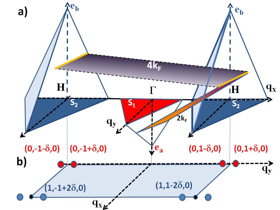
The origin of SDW in chromium is now clear and arises from the peculiar geometry its Fermi surfacefawcett ; kevan . It is based on a nesting effect between the electron pocket centered at point and the hole pocket centered at the edge of the Brillouin zone at point (see Fig. 1)overhauser . Note that the two pockets do not have the same size and this size difference explains the presence of a SDW in chromium.
In contrast, the physical origin of the CDW in chromium is still not understood. Two scenarios may be considered. Either the CDW is induced by a magnetostriction effect (a coupling between elasticity and magnetism) or by a purely electronic effect based on nesting between electronic bandsyoungsokoloff .

The average behavior of chromium does not contradict the magnetostriction scenario. Classical diffraction experiments provide spatially averaged information that show that both CDW and SDW appear simultaneously at the same Néel temperature = 311K. Micro-diffraction experiments have also shown that their domains are highly correlatedevans and that spin and charge orders are similarly suppressed with pressurefeng . Other studies, using diffraction techniques, tried to answer this issue without being able to clearly discriminate between the two scenariosmori .
We show in this paper that a precise comparison of the spatial fluctuations of each modulation allows us to reconsider the origin of CDW in chromium. Indeed, this first experiment combining coherent and simultaneous X-ray diffraction shows that defects affect the charge order but not the spin one and hence that spin and charge orders in chromium have the same origin: a purely electronic effect due to the peculiar band structure of chromium.
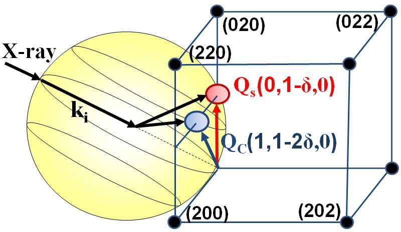
Classical X-ray diffraction is a powerful technique to probe the charge and the spin modulation of chromium because the SDW period is twice larger than the CDW one, and the two satellite reflections can be measured independently at and at wave vectors. In ref hill , the profiles of the two satellites reflections indicates that the CDW coherence length is smaller than the SDW one.
However, a precise comparison of correlation lengths of coexisting phases is difficult by diffraction techniques since the probed volumes are usually not the same. In the case of chromium in hill , the volume probed at is much smaller that the one probed at note1 which makes the comparison of the two correlation lengths only qualitative.
We have used here a combination of two techniques to go beyond these limitations. Coherent x-ray diffraction has been performed to measure spatial fluctuations of the two modulations without spatial average and simultaneous diffraction to probe CDW and SDW in the same sample volume.
A coherent x-ray beam has been obtained from a weakly coherent synchrotron source by using a set of two slits. The first one is located just after the optics to get rid of optical aberrations and the second one at 15 cm upstream of the sample.

Thanks to this setup and using appropriate apertures, a 10 m x-ray beam with degree of coherence is obtained. The experimental setup used for coherent diffraction experiments is described in details in lebolloch3 and the ability of this technique to probe charge density wave systems in jacques2 . The experiments have been performed at the Cristal beam line of synchrotron Soleil and at the ID20 beam line of the ESRF using an energy of E=5.9 keV, just below the chromium -edge to avoid fluorescence. A single- domain chromium sample has been probed in reflection geometry with in reciprocal lattice units (r.l.u.) at T=140 K.
To fulfill simultaneous diffraction conditions, the sample is placed in such a way that the and the satellites are simultaneously located on the Ewald sphere. Therefore, both reflections can be measured by moving only the detector and not the sample. As a consequence, the beam location on the sample’s surface and the volume probed by the beam are equal for the two satellites.

The three diffraction patterns displayed in Fig. 2 give a clear picture of the SDW and CDW states in chromium. No speckle is observed at the satellite reflection associated to the SDW. The pattern displays a single peak, the width of which corresponds to the footprint of the beam at the sample surface (Fig. 3a and Fig. 3c). The fundamental (0 1 1) reflection associated to the lattice displays also a single peak with an equal width. In contrast, the satellite associated to the CDW is broader and displays speckles (see Fig. 3b).
The interpretation is clear and unequivocal: the SDW in chromium displays a impressive long range order, without domains or phase shifts, over the entire probed volume, i.e. 10107m (in depth). Note that a single phase shift of the magnetic order would induce a splitting of the satellite reflection in Fig.3c)silicon . On the contrary, in the same volume, the CDW displays phase shifts. This measurement proves that, contrary to the charge one, the spin order is unaffected by the presence of punctual defects such as interstitials or/and vacancies which are abundant in such a large volume. This conclusion differs from that of ref. naturechromium in which the authors interpret the presence of speckles on the CDW reflection as a consequence of the presence of magnetic domain walls. In our case, the sample is single-Q and speckles are present on the CDW reflection and not on the SDW reflection. Thus, in our case, the presence of speckles on the CDW reflection can not be explained by the presence of antiferromagnetic domains.
This comparison between charge and spin orders is crucial to better understand the origin of both states. How can we explain that, despite the strong relationship between SDW and CDW in chromium, the spin correlation length remains long-range while the charge one is much smallerhabibi ? In the following, the two scenarios mentioned in the introduction are discussed in the light of our experimental results.
Magnetostriction is the most frequently cited scenario to account for the presence of CDW in chromium. The appearance of a periodic lattice distortion within a magnetic order may reduce the total energy. In that case, three contributions have to be considered: the anisotropy energy (), the exchange energy () and the elastic cost due the periodic distortion ():
where is the magnetic momentum of the atom, the atomic displacement with respect to the non-magnetic structure, depends of the distance between planes and , the force constant and the kinetic momentum. In chromium, the lowest total energy is found when the CDW period is twice shorter than that of SDW, in agreement with experimentsnourtier . The main point here is that the energy minimization gives a close relationship between CDW and SDW: spatial fluctuations of the first lead to spatial fluctuations of the second and reciprocally. From this point of view, the magnetostriction scenario seems hardly compatible with our experimental data displayed in Fig. 3.
In the following, we consider the second scenario introduced by Young & Sokoloff in youngsokoloff based on a three-band model. We show that this model, in the presence of punctual defects, is in agreement with our measurement. In this approach, the CDW is the second harmonic of SDW. More generally, these authors have shown that odd harmonics are spin orders and even ones are charge orders.
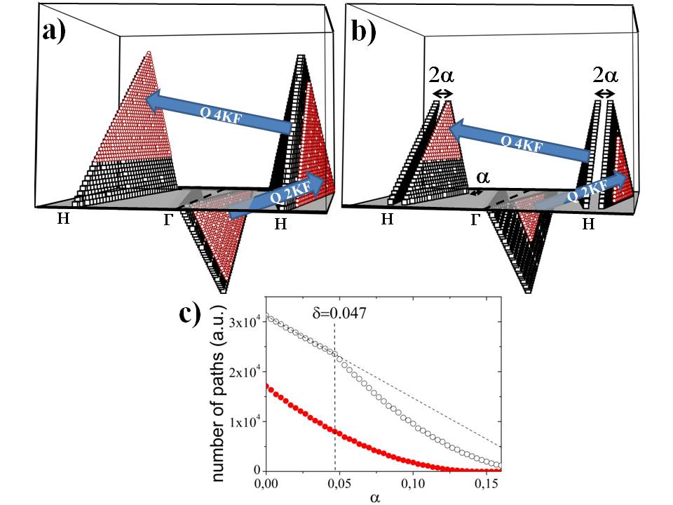
In this purpose, inelastic nesting between bands has been considered as in fishman and linear dispersion curves for electrons () and holes () have been assumed. We thus have to consider three prisms and connect the four surfaces of each of them. The model is adjusted to the case of chromiumRefJ3 ; the size of the electron () and hole () pockets is such as . The two Fermi velocities ( and ) have also been extracted from experimental data. The three corresponding prisms with maximum energies and are drawn of Fig. 1.a and in Fig. 4a. For a strict coexistence of both phases such as measured in chromium, a simultaneous nesting is authorized between the electron and the hole pockets with and between the two hole pockets at . The three-band hamiltonian reads:
where is the SDW order parameter and the CDW order parameter. The linear temperature dependence of has been extracted from fawcett . The Green function can be extracted from following the standard BCS equation:
Making the summation of and over all Matsubara frequencies, one finds two simultaneous gap equations
| and | ||||
where , and are the three zeros of , , is the coupling constant between electron and hole and the coupling between holes. We are looking for simultaneous solutions of the two gap equations corresponding to a stable thermodynamical phase. Solutions of each gap equation separately correspond to single (spin or charge) phases, when the other order parameter is suppressed.

The integration in the plane taking into account all nesting processes corresponds to the summation over the 4 surfaces of each prism. Considering only one surface out of four, the process is described in Fig. 4a where the points fulfilling simultaneously both conditions ( and along the [010] direction only) are represented with red circles. Note that the electron surface, which is smaller, constrains the hole surface and restricts the total number of nested points. Within this model, we correctly reproduce the mixed state in chromium and the Néel temperature of T=311K. A paper detailing theoretical aspects will be published elsewhere.
In this approach, CDW is the second harmonic of SDW and will be more sensitive to punctual defects in agreement with our measurement. One can simply understand this greater sensibility by considering the influence of punctual defects on the three prims of Fig. 1. Indeed, similarly to phonons in the presence of punctual defectsnote2 , we consider that the dispersion curves will be mainly affected at the border of Brillouin zone. Therefore, only the two hole pockets centered at points will be affected and not the electron one at . To take into account this effect, we remove from nesting processes the states located in two wide stripes (one along and one along ) centered at points (see Fig. 4b). As a consequence, the contribution of the second order nesting in the total energy is strongly reduced with respect to the contribution of the first order one. This statement becomes clear if the number of authorized paths between bands is taken into account: the number of paths between the two hole pockets decreases much more sharply than the number of paths between the electron and hole pockets for increasing . Since the two holes areas are affected by punctual defects, the first one decreases as , while the second one decreases as linearly for (see Fig. 4c).
In conclusion, an original experiment coupling coherent x-rays and simultaneous diffraction has been performed to precisely measure correlation lengths in chromium. The SDW does not display any dislocation over several micrometers in the sample while the CDW one displays many speckles. This observation is a clear misstatement of the usually accepted magnetostriction theory. We explain these experimental features using the Young and Sokoloff model where the CDW and the SDW are coming from the same phase with the CDW being a second harmonics of the SDW. This second harmonic theory and the peculiar band structure of chromium makes the CDW more sensitive to punctual defects, in agreement with our measurement. From this approach, we predict that in the limit case, in the presence of many uncorrelated defects, a new phase of chromium should stabilize SDW with no CDW. In this framework, the wave vector is not associated to a simple strain wave but to a true incommensurate CDW linked to a periodic lattice distortion. From this point of view, the CDW in chromium should slide under an external current.
References
- (1) G. Ghiringhelli et al., Science 337, 821 (2012).
- (2) P. Diener, M. Leroux, L. Cario, T. Klein, P. Rodière Phys. Rev. B 84, 054531 (2011); T. Kiss et al., Nature Physics 3, 720 (2007).
- (3) G. Abramovici, T. Vinatier and M. Héritier, Solid State Commun. 169, 42 (2013).
- (4) J. P. Hill, G. Helgesen, and D. Gibbs, Phys. Rev. B 51, 10336 (1995).
- (5) The x-ray penetration is in depth at and at at the incident energy E=5.9 KeV.
- (6) D. R. Noakes, T. M. Holden, E. Fawcett, and P. C. de Camargo Phys. Rev. Lett. 65, 369 (1990); E. Fawcett, R. B. Roberts, R. Day, and G. K. White, Europhys. Lett. 1, 473 (1986); P. C. de Camargo, E. P. Castro and E. Fawcett., J. Phys F 18 : L209 (1988).
- (7) J. Schäfer, Eli Rotenberg, G. Meigs, and S. D. Kevan, P. Blaha, and S. Hüfner, Phys. Rev. Lett. 83, 2069 (1999); E. Rotenberg, O. Krupin and S. D. Kevan, New J. Phys 10, 023003 (2008);M.-A. Leroy, A. M. Bataille, F. Bertran, P. Le Fèvre, A. Taleb-Ibrahimi, and S. Andrieu, Phys. Rev. B 88, 205134 (2013).
- (8) A. W. Overhauser, Phys. Rev. 128, 1437 (1962).
- (9) C. Y. Young and J. B. Sokoloff, J. Phys. F: Metal Phys. 4, 1304 (1974).
- (10) X W Jiang and R S Fishman 1997, J. Phys.: Condens. Matter 9 3417.
- (11) M. Mori and Y. Tsunoda, J. Phys.: Condens. Matter 5 L77 (1993); D. Lamago, M. Hoesch, M. Krisch, R. Heid, K.-P. Bohnen, P. Boni, and D. Reznik, Phys. Rev. B 82, 195121 (2010).
- (12) P. G. Evans, E. D. Isaacs, G. Aeppli, Z. Cai, B. Lai, Science 295, 1042 (2002).
- (13) Y. Feng, R. Jaramillo, G. Srajer, J. C. Lang, Z. Islam, M. S. Somayazulu, O. G. Shpyrko, J. J. Pluth, H.-k. Mao, E. D. Isaacs, G. Aeppli, and T. F. Rosenbaum, Phys. Rev. Lett. 99, 137201 (2007).
- (14) V. L. R. Jacques, D. Le Bolloc’h, E. Pinsolle, F. E. Picca, and S. Ravy, Phys. Rev. B 86, 144117 (2012); D. Le Bolloc’h and J. F. Sadoc, Eur. Phys. J. B 81, 481-487 (2011); D. Le Bolloc’h, F. Livet, F. Bley, T. Schülli, P. Marion, H. T. Metzger, J. Synch. Rad. 9, 258-265 (2002).
- (15) V. L. R. Jacques, D. Le Bolloc’h, S. Ravy, J. Dumas, C. V. Colin, and C. Mazzoli, Phys. Rev. B 85, 035113 (2012); V. L. R. Jacques, D. Le Bolloc’h, S. Ravy, C. Gilles, F. Livet and S. B. Wilkins, Eur. Phys. J. B 70, 317 (2009); E. Pinsolle, N. Kirova, V. L. R. Jacques, A. A. Sinchenko, and D. Le Bolloc’h, Phys. Rev. Lett. 109, 256402 (2012).
- (16) V. L. R. Jacques, S. Ravy, D. Le Bolloc’h, E. Pinsolle, M. Sauvage-Simkin, and F. Livet, Phys. Rev. Lett. 106, 065502 (2011).
- (17) O.G. Shpyrko, E.D. Isaacs, J.M. Logan, Y. Feng, G. Aeppli, R. Jaramillo, H.C. Kim, T.F. Rosenbaum, P. Zschack, M. Sprung, S. Narayanan, and A.R. Sandy, Nature 447, 68 (2007).
- (18) P Habibi, C Barreteau and A Smogunov, 2013 J. Phys.: Condens. Matter 25 146002.
- (19) C. Nourtier, Journal de Physique, 34 57 (1973); T. Nishikubo, T. Nagamiya, J. Phys. Soc. Jap. 20 (1965) 808; Y. Tsunoda, M. Mori, N. Kunitomi, Y. Teraoka and J. Kanamori, Solid States Commun. 14, 287 (1974).
- (20) E. Fawcett, Rev. Mod. Phys. 60, 209 (1988).
- (21) see for example: D. Le Bolloc’h, J. L. Robertson, H. Reichert, S. C. Moss, and M. L. Crow, Phys. Rev. B 63, 035204 (2001) and references therein.