Localized Surface Plasmon Resonance in SnS:Ag Nano-composite Films
Abstract
Nano-composite films of Tin Sulfide (SnS) and silver (Ag) fabricated by thermal evaporation showed two prominent peaks in the visible region of their extinction spectra. Theoretical modeling of the extinction spectra suggest that these two peaks ( and ) correspond to the longitudinal mode (LM) and transverse mode (TM) surface plasmon resonance peaks arising from oblate silver nano-particles. Using grain size of silver and SnS obtained from structural and morphological characterizations of the samples and dielectric constants as per actuals, we have compared the experimental results with those from theory. The study shows that silver nano-particles efficiently scatters light and can be used for developing plasmonic based SnS solar cells with improved efficiencies.
keywords:
Thin Films; Chalcogenides; Optical properties1 Introduction
Thin film photo-voltaic devices made of inorganic semiconductors such as Tin Sulfide (SnS) and Cadmium Telluride (CdTe) etc. have gained attention in recent years due to their lower cost compared to the made from Silicon [1, 2, 3]. SnS is consider a better option considering they are not toxic like Cadmium compounds [4]. SnS is a semiconducting material that has a band-gap ranging between 1.1-2.2 eV [5, 6] and refractive index in the range of 1.6-2.2 eV, depending on the fabrication techniques [7, 8]. However, the major limitation of inorganic semiconductors are their light trapping ability thereby which their efficiency as solar cells are lowered (compared to Silicon) [9]. In order, to increase the light trapping ability of these semiconductors, researchers are adopting a new methods using noble metal nano-particles dispersed in the semiconducting film [9, 10].
Noble metal nano-particles like silver (Ag), gold (Au), aluminum (Al) and copper (Cu) embedded in a dielectric/semiconducting medium exhibit interesting optical properties and have gained a lot of attention due to their potential applications in plasmonic solar cells [9], photonic devices [11], surface plasmon enhanced sensors [12]. Localized Surface Plasmon Resonance (LSPR) occurs when the electromagnetic wave travels along the metal and dielectric/ semiconductor interface [13]. LSPR peaks and their positions are influenced by the size, the shape of the metal nano-particle [14], its dielectric properties and those of the local surrounding medium . For nano-particles of Ag, Au and copper the LSPR peak occurs in the UV-Visible region of the spectrum depending on the density of the electrons in the metal nano-particle[12, 15]. Literature consists of many articles on metal nano-particles embedded in different dielectric/semiconducting mediums like [16], Si [13] and ZnO [17] etc. Out of all the noble metals, silver nano-particles showed the best SPR response [18], making it very useful for applications. We hence selected Ag to study the surface plasmon resonance in Tin Sulfide (SnS). Very few research groups have carried out work on Ag-SnS films [19, 20, 21]. In this manuscript, we report the preparation of SnS:Ag nano-composite films of varying thicknesses and investigate the size-dependent optical properties.
2 Experimental Details
Composite thin films of Tin sulfide (SnS) and silver (Ag) were grown by thermal evaporation with vacuum better than Torr. The pellets used as starting material were made by mixing SnS powder and Ag nano-powder (average grain size 20 nm). The mass ratio of SnS and Ag powder used was 2:1. The 99.99% purity SnS powder was provided by Himedia (Mumbai) and the Ag nano-powder was obtained from Nanoshel (USA). The thickness of the films were measured using Veeco’s Dektak Surface profiler (150). The structural properties of the films were studied using a Bruker D8 diffractometer at an operating voltage of 40 KV in the mode with Cu target giving X-Ray at and Technai G2 T30U Twin Transmission Electron Microscope (TEM) at an accelerating voltage of 200 KV. The chemical composition analysis of the films were examined using Kratos Axis Ultra DLD’s X-Ray Photo-electron Spectroscopy (XPS) with Al target. The beam energy used for the analysis was 1490 eV and binding energy was referenced with respect to Carbon. The surface morphology was analyzed by a Field Emission Scanning electron Microscopy (FE-SEM FEI-Quanta 200F). The optical absorption and transmittance spectra were recorded using a Systronics UV-VIS Double beam spectrophotometer (2202) in the 300-900 nm wavelength range.
3 Results and Discussion
3.1 Experimental Results
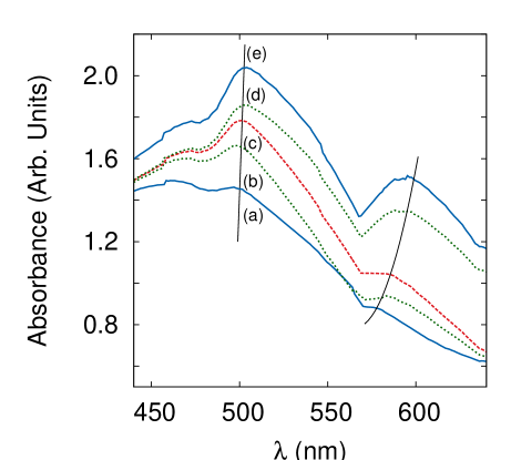
Figure 1 shows the optical absorption spectra of the SnS/Ag composite thin films. Unlike the absorption spectra of SnS films [6], these films show two peaks at and in all the films without exception. Considering the starting silver powder had particle size of 20 nm, we believe these peaks are Localized Surface Plasmon Resonance (LSPR) peaks resulting from interaction of light with electrons at the surface of the silver nano-particles [22, 23]. Considering that the LSPR peak position depends on the surrounding media’s refractive index along with the shape and size of the metal cluster, the existence of two well resolved peaks in fig 1 may either be due to non-spherical metallic clusters or because they experience two different surrounding media (possibly air and SnS). Another interesting feature of fig 1 is that both peaks show red-shift, however it is more pronounced in the peak.
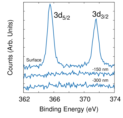

Before proceeding, we would have to resolve whether silver nano-particles are uniformly distributed throughout the thickness of the film or not. We have used depth profiling using X-ray Photo-electron Spectroscopy (XPS). Fig 2 shows the XPS scan for Ag (Ag 3d peak) [24, 25] at the film’s surface, at 150 and 300 nm below the surface of a 600 nm thick SnS:Ag nano-composite film. Comparing the scans, we find that the XPS peaks of silver completely vanishes below 150 nm from the surface of the film. This clearly implies that the silver nano-particles are only present on and adjacent to the surface of the films. The deposition of Ag on the surface or just below is due to the higher melting point of Ag (1234 K) compared to (1155 K) that of SnS [26, 27]. Varying the rate of evaporation does give an uniform distribution of silver along the thickness of the SnS film. However, since this study is a part of a continuous evaluation of SnS and their nano-composite films, we have maintained the film fabrication parameters as in our earlier studies [8, 28, 29]. The existence of Ag at the surface (in contact with air-SnS interface) and within the SnS surface presents a possibility of two LSPR peaks in the UV-visible absorption spectra which we shall resolve in our theoretical analysis.
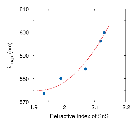
As stated above, the 580 nm absorption peak of fig 1 shows a strong red-shift which increases with increasing film thickness. An interesting aspect about LSPR peaks is that its position strongly depends on the refractive index of the surrounding media. An increasing refractive index of the surrounding dielectric results in a red-shift [30]. Hence, clearly, we expect that the SnS film’s refractive index increases with increasing film thickness. To investigate the possible cause of increase in SnS refractive index with film thickness, we investigate the structural properties of samples. Fig 3 shows the diffraction patterns of various thickness SnS:Ag nano-composite films. Without exception all the films showed polycrystallinity with SnS having orthorhombic structure with lattice parameters matching those given in ASTM Card No 83-1758 while Ag matched those given in ASTM Card No 03-0931. The grain size of SnS and Ag nano-particles were evaluated using the Scherrers formula [31]. We shall be commenting on the grain size of silver nano-particles below, however the SnS grains showed a linear increase in grain size with increasing film thickness. In earlier studies [8, 28, 29] we conducted on thin SnS films (without Ag) grown under identical conditions, we had reported the optical properties of SnS films as a function of grain size. We had reported that the SnS film’s refractive index increased with increasing grain size, which in turn increased with film thickness (fig 6 of ref [8]). We find that the SnS grain size (12-19 nm) and its variation with film thickness in these nano-composite films matched (within experimental error) with previous studies. As stated initially, we believe that the increasing refractive index with increasing thickness of SnS background contributes to the observed red-shift in the 580 nm LSPR peak of fig 1. As explained above, we use experimentally evaluated refractive index of SnS films as a function of film thickness and plot position of the SPR peak () with respect to it (fig 4). Notice that the variation is similar to that shown in fig 1. The experimentally evaluated values of refractive index would hence be utilized as input parameters for the Gans model calculations we discuss in the next section. Also, we notice only a small variation in refractive index with SnS grain size for explaining the insignificant or minor red-shift seen in the peak.
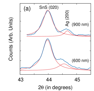
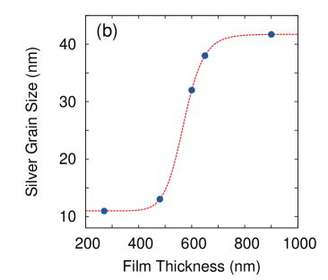
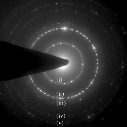
Other then the XPS results, the lone XRD peak of Ag also confirms the existence of metallic clusters of silver in the nano-composite films. Further proof of metallic Ag clusters in our samples come from the electron diffraction rings (Selected Area Electron Diffraction, SAED image) obtained using the Transmission Election Microscope. SAED pattern (fig 5) shows two sharp rings corresponding to two prominent peaks from Ag. The two Ag rings marked (i) and (ii) in fig 5 correspond to the (200) and (220) planes. The remaining three rings of fig 5, marked (iii), (iv) and (v), correspond to the (040), (131) and (200) diffraction planes of SnS. An investigation of the diffraction patterns at and , of fig 3, shows them to be resolvable peaks of SnS and Ag (fig 6a). The peaks were de-convoluted and the average grain size of silver nano-particles were evaluated using the Scherrer’s formula. Fig 6b shows the variation in the silver nano-particle grain size with film thickness. Notice that the average size of the Ag nano-particle is around 12 nm for films with thickness less than 600 nm while they are in the range of 32-42 nm for higher thickness films. As the size of the metal cluster increases there is an increase in radiative damping that leads to greater scattering cross-sections and hence larger extinction [9].
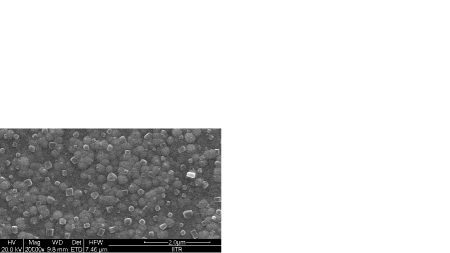
Fig 7 exhibits a SEM micrograph of a 650 nm thick SnS:Ag nano-composite film. As viewed from the surface, micrograph shows that the film consists of randomly spaced cuboid silver nano-particles [32] dispersed among nearly spherical SnS nano-particles of SnS. The chemical composition of the grains were confirmed using the EDAX (Energy Dispersive Analysis of X-ray) attachment with the scanning electron microscope.
3.2 Theoretical Consideration
The extinction spectra of fig 1 can be theoretically generated using various computational models, like Mie Model [33], Gans Model [34, 35] and Discrete Dipole Approximation (DDA) Model [36, 37]. Mie theory was developed to study scattering due to spherical particle [33]. The model was successfully extended for studying Localized Surface Plasmon Resonance due to spherical metal nano-particles dispersed in semiconducting or insulating media. However, the model needed corrections to include non-spherical shaped metal clusters. The modifications proposed by Gans [34, 35]. Considering that our SEM morphology images suggest our silver metal clusters to have near square cross-section on the surface () and XPS results suggest the grains to occur only on the film surface, we expect i.e. the silver nano-particles are oblate shaped with size less than 50 nm. We have, hence used Gans model to theoretically analyze our experimental results.
Gans model gives the extinction cross-section/ coefficient which is the sum of light intensity scattered and absorbed by a metal nano-particle whose shape is either oblate or prolate. The scattering and absorption cross-sections are calculated using [9]
| (1) |
and
| (2) |
where,
| (3) |
where, ‘L’ is the depolarization factor that depends on the shape of the scattering/ absorbing metal nano-particle, ‘V’ is the volume of the nano-particle, ‘’ is the complex dielectric constant of the metal and ‘’ is that of the surrounding medium. For non-sphere clusters, the depolarization factor ‘L’ takes different values along the three axes. The values completely depend on the shape of the metal nano-particle which is mathematically defined by the aspect ratio (ratio of minor to major axis of the spheroid). For an oblate nano-particle () it is given as
Where ‘e’ is related to the aspect ratio
Eqn 3 is now written as
| (4) |
When an E-M radiation is incident on a spheroid nano-cluster, electrons are set into oscillations along and perpendicular to its symmetry axis, resulting in two plasmon resonance peaks. Each peak is associated with the oscillation direction with respect to the symmetry axis and are named as the longitudinal mode (LM) and the transverse mode (TM) [38]. In the case of oblate nano-clusters the TM excitations appear at higher wavelengths compared to that of the LM excitations [38]. Expectedly, the separation between the two modes depend on how much deviation the spheroid has from an ideal sphere, or in other words depends on the cluster’s aspect ratio and the refractive index of the surrounding medium [14, 38].
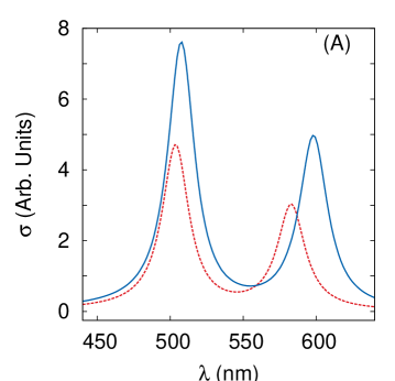
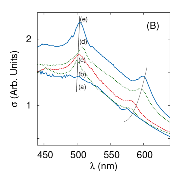
Our calculations for extinction coefficients were done using the complex dielectric constant for silver listed as a function of wavelength by Palik et al [39]. We used the data from fig 6 for estimating the grain size of silver. Before calculating case of silver dispersed in SnS, simulation was done for silver in air. Our calculations agreed with literature [17] and found LSPR peak appear at 350 nm. Thus, we can confidently rule out silver-air interface playing a role in this study. We hence proceed reporting effect of Ag-SnS interface in this study. The results of Priyal et al [28, 8] were used for the SnS background’s dielectric constant. The studies showed SnS film’s refractive index follow a trend similar to the Cauchy’s dispersion relation [40] with the wavelength, where the coefficients strongly depend on SnS grain size. Fig 8 shows the extinction spectra generated theoretically. The aspect ratio was linearly varied from 0.64 to 0.60 with increasing film thickness. The values were selected so that peak positions obtained theoretically matched with the experimentally obtained results. Fig 8A shows select calculated extinction coefficient spectra. These spectra are of course quite dissimilar from those shown in fig 1 since fig 1 also contains the absorption spectra of the background SnS film. To recreate fig 1 we have super-imposed data of fig 8A on absorption spectra of SnS films of corresponding thicknesses with same/similar grain size used in our previous studies [28]. We may hence conclude that the peaks of fig 1 at and correspond to the longitudinal and transverse modes respectively. Fig 8B gives thus theoretically simulated spectra and we find them in fairly good agreement with the experimentally obtained data of fig 1. Fig 8B also includes the two trend lines of fig 1 to show how well our simulations agree with experimental data.
The above results clearly establishes the formation of LSPR peaks in SnS:Ag nano-composite films. It is of immense interest that the well established theory easily quantifies the experimental observations. As stated, SnS films have attracted interest in recent years for its application as photovoltaics [41, 42]. While their properties of being non-toxic and films with good absorption and high band-gap make them suitable candidates, attempts of fabricating photovoltaics show that they do not match the efficiency of silicon [41, 43]. A basic issue with thin film solar cell devices is that the absorbing layer being thin does not absorb sufficient amount of light for charge carrier generation and hence leads to low efficiency. Hence, research has been directed towards plasmonic solar cells of SnS. One expects that the metal nano-particles in the medium would at resonant frequency either absorb the incident light or scatter it within the medium [9, 44]. If scattering can be made the dominant extinction mechanism, the efficiency of the device can be enhanced [9]. Using the above made calculations (namely using eqn 1 and 2), we have calculated the scattering efficiency () using
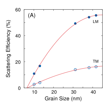
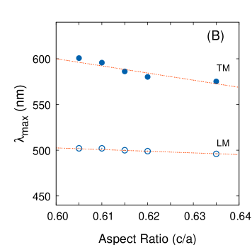
Fig 9A shows scattering efficiency of the LM and TM peaks. The scattering efficiencies vary as a (quadratic) function of the grain size and are marked different for the LM and TM modes. The scattering contribution is more in the LM peak as compared to that of the TM peak. Fig 9A is misleading since grain size only contributes to extinction’s intensity via the volume term of eqn 3. Size indirectly influences the scattering efficiency through the real component of silver’s dielectric constant () and SnS background’s dielectric constant (). Both these factors vary with respective grain size (silver and SnS) which are in turn dependent on the film thickness. As the film thickness increase, the grain size of silver and SnS increases. This results in increased difference in silver’s and SnS’s dielectric constant, resulting in stronger scattering from the metal nano-particles (also understood from eqn 4). This is possibly due to the fact that the effective size of the metal nano-particle increases as the refractive index of SnS increases leading to larger scattering. The result is promising considering that we now can predict and material manipulate plasmonic layer to obtain high efficiency solar devices. Another aspect of interest for device fabrication would be to bring the two resolved peaks close by. This would result in an absorption band leading to a range of wavelengths being captured and scattered within the medium encourage easy electron-hole pair generation. It is the non-spherical shape of the metal nano-clusters (aspect ratio ) that gives rise to the two peaks. This is best understood by investigating the peak positions () as a function of aspect ratio (fig 9B). Both, the LM and TM peaks show blue shifts with increasing aspect ratio (c/a), this trend is in agreement to those reported in literature [38]. The dotted lines indicate the trends and suggest that they would tend to converge around 0.75, for which we would have the TM and LM peaks close by resulting in a board absorption band.
In conclusion, we can relate all of the above results. For an efficient photo-layer of a solar device, we ideally require SnS:Ag nano-composite films with 40 nm sized silver metal nano-clusters which are oblate shaped with aspect ratio of 0.75 and large sized SnS grains. This ensures a large difference in SnS and silver refractive indices that lead to enhanced scattering of light within the films and the aspect ratio ensure unresolved TM and LM peaks giving broad absorption band.
Conclusion
Nano-composite films of SnS and Ag were grown on glass substrates at room temperature. The films showed two prominent peaks at and in their UV-visible spectra. These peaks showed a red-shift as the film thickness increased. Structural studies reveal increase in Ag and SnS nano-particle size with increasing film thickness. We were able to generate the observed extinction spectra using Gans model. The results of our calculations suggest that the and corresponds to the longitudinal and transverse mode LSPR peaks from oblate silver nano-particles. The theoretical and experimental results also explains the observed red shift in the SPR peak at due to the increasing refractive index of the background SnS. Theoretical results also suggests that as the aspect ratio of Ag nano-particles decreases with increasing film thickness, the two resonant peaks move away from each other. The calculations also explain the increase in scattering efficiency with increasing Ag nano-particle size as resulting from enhanced difference between the metal and its background’s dielectric constant. Both theoretical and experimental results suggest that one can tailor the SPR peak positions and scattering efficiency of such nano-composites. SnS:Ag nano-composite films hence present itself as an efficient photo-layer in solar voltaics. Based on our results we suggest SnS:Ag nano-composite films with oblate shaped (aspect ratio ) Ag nano-particles of size around 40 nm which embedded in large grain sized SnS background would prove ideal for plasmonic devices.
Acknowledgement
Authors are thankful to the University Grants Commission (UGC, India) for funding this work under their Major Research Project Scheme (F.No. 39-531/2010SR).
References
- [1] Ristov M., Sinadinovski G., Mitreski M., Ristova M., Photovoltaic cells based on chemically deposited p-type SnS, Sol. Energy Mater. Sol. Cells, 69 (2001) 17.
- [2] Oladeji I.O, Chow L., Viswanathan V., Zhao Z., Metal/CdTe/CdS/Cd1xZnxS/TCO/glass: A new CdTe thin film solar cell structure, Sol. Energy Mater. Sol. Cells, 61 (2000) 203.
- [3] Frantzis L., Jones E., Little A.D., Lee C., Wood M. and Wormser P., 16th Eur. Photovoltaic Sol. Energy Conf. (Proceedings), Glasgow, Scotland, (2000) 2103.
- [4] Reddy K.T.R., Reddy N.K., Miles R.W., Photovoltaic Properties of SnS based solar cells. Sol. Energy Mater. Sol. Cells, 90 (2006) 3041.
- [5] Gao C, Shen H, Sun L. Preparation and properties of zinc blende and orthorhombic SnS films by chemical bath deposition, Appl. Surf. Sci., 257 (2011) 6750.
- [6] Sohila S., Rajalakshmi M., Ghosh C., Arora A.K. and Muthamizhchelvan C., Optical and Raman scattering studies on SnS nanoparticles, J. Alloys Compd. 509 (2011) 5843.
- [7] Shaaban E.R., El-Sadek M.S.A, El-Hagary M. and Yahia I.S., Spectroscopic ellipsometry investigations of the optical constants of nanocrystalline SnS thin films, Phys. Scripta 86 (2012) 015702.
- [8] Jakhar A., Jamdagni A., Bakshi A., Verma T., Shukla V., Jain P., Sinha N. and Arun P., Refractive index of SnS thin nano-crystalline films, Solid State Commun., 168 (2013) 31.
- [9] Catchpole K.R. and Polman A., Plasmonic solar cells, Optic. Express, 16 (2008) 21793.
- [10] Catchpole K. R. and Polman A., Design principles for particle plasmon enhanced solar cells, Appl. Phys. Lett. 93 (2008) 191113.
- [11] Sundararajan S.P., Grady N.K., Mirin N. and Halas N.J., Nanoparticle-Induced Enhancement and Suppression of Photocurrent in a Silicon Photodiode, Nano Lett., 8 (2008) 624.
- [12] Lee K.S. and El-Sayed M.A., Gold and Silver Nanoparticles in Sensing and Imaging: Sensitivity of Plasmon Response to Size, Shape, and Metal Composition, J. Phys. Chem. B, 110 (2006) 19220.
- [13] Pillai S., Catchpole K.R., Trupke T., and Green M.A., Surface plasmon enhanced silicon solar cells, J. Appl. Phys. 101 (2207) 093105.
- [14] Kelly K.L., Coronado E.,l Zhao L.L. and Schatz G.C., The Optical properties of metal nanoparticles: The Influence of size, shape and Dielectric Enviornment, J. Phys. Chem. B, 107 (2003) 668.
- [15] Link S. and El-Sayed M.A., Size and Temperature Dependence of the Plasmon Absorption of Colloidal Gold Nanoparticles, J. Phys. Chem. B, 103 (1999) 4212.
- [16] Kiran P.P., Bhakth B.N.S., Rao D.N. and De G., Nonlinear optical properties and surface-plasmon enhanced optical limiting in Ag–Cu nanoclusters co-doped in SiO2 Sol-Gel films, J. Appl. Phys., 96 (2004) 6717.
- [17] Islam M.A. and Khan I., ZnO/Ag Composite Nanoparticles for Surface Plasmon Resonance Based Sensor Application in UV-Vis Region, International Journak Of Advancements in Research and Technology, 1 (2012) 1.
- [18] Pustovit, Vitaliy N, Shahbazyan, Tigran V, Finite-size effects in surface-enhanced Raman scattering in noble-metal nanoparticles: a semiclassical approach, J. Opt. Soc. Am. A, 23 (2006) 1369.
- [19] Jia H.J., Cheng S.Y., Wu X.K. and Yang Y.L., Effect of anneal temperature on electrical and optical properties of SnS:Ag thin films, Natural Sci., 2 (2010) 197.
- [20] Yongli Y. and Shuying C., Preparation of SnS:Ag Thin Films by Pulse Electrodeposition, J. Semicond., 29 (2008) 2322.
- [21] Lu P., Jia H. and Cheng S., Optical and Elctrical Properties of SnS:Ag Films as Solar Cell Absorbers, Adv. Mater. Res., 60 (2009) 11.
- [22] Singh Y.P., Jain A. and Kapoor A., Localized Surface Plasmons Enhanced Light Transmission into c-Silicon Solar Cells, J. Sol. Energy (2013) 584283-1.
- [23] Awazu K., Fujimaki M., Rockstuhl C., Tominaga J., Murakami H., Ohki Y. , Yoshida N. and Watanabe T., A Plasmonic Photocatalyst Consisting of Silver Nanoparticles Embedded in Titanium Dioxide, J. Am. Chem. Soc. 130 (2008) 1676.
- [24] Morales J., Sanchez L., Martın F., Ramos-Barrado J.R. and Sanchez M., J. Electrochem. Soc., 151 (2004) A151.
- [25] Prieto P., Nistor V., Nouneh K., Oyama M., Abd-Lefdil M. and Díaz R., XPS study of silver, nickel and bimetallic silver–nickel nanoparticles prepared by seed-mediated growth, Appl. Surf. Sci., 258 (2012) 8807.
- [26] Lide D.R., ed., CRC Handbook of Chemistry and Physics, Internet Version 2005.
- [27] Thangaraju B. and Kaliannan P., Spray pyrolytic deposition and characterization of SnS and SnS2 thin films, J. Phys. D: Appl. Phys. 33 (2000) 1054.
- [28] Jain P. and Arun P., Parameters influencing the optical properties of SnS thin films, J. Semicond., 34 (2013) 093004-1.
- [29] Jain P. and Arun P., Influence of grain size on the band-gap of annealed SnS thin films, Thin Solid Films, 548 (2013) 241.
- [30] Takeda Y., Plaksin O.A., Wang H., Kono K. Umeda N. and Kishimoto N., Surface Plasmon Resonance of Au nano-particles fabricated by negative Ion implantation and Grid structure towards Plasmonic Applications, Optical Rev. 13 (2006) 231.
- [31] Cullity B D, Stock S R., Elements of X-ray diffraction. 3rd Ed. NJ: Prentice-Hall Inc, 2001.
- [32] Wiley B.J., Im S.H., Li Z.Y., Mc Lellan J., Sickkinen A. and Xia Y., Maneuvering the surface plasmon resonance of silver nanostructures through shape-controlled synthesis, J. Phys. Chem. B, 110 (2006) 15666.
- [33] Fu Q., Sun W., Mie theory for light scattering by a spherical particle in an absorbing medium, Appl. Optics, 40 (2001) 1354.
- [34] Ranjan M., Predicting plasmonic coupling with Mie–Gans theory in silver nanoparticle arrays, J. Nanopart. Res., 15 (2013) 1.
- [35] Heilmann A., Quinten M. and Werner J., Optical Response of thin plasma- polymer films with non-spherical silver nano-particles, The European Phys. J. B-Cond. Mat. and Complex systems, 3 (1998) 455.
- [36] Draine B.T. and Flatau P.J., Discrete-dipole approximation for scattering calculations, J. Opt. Soc. Am. A., 11 (1994) 1491.
- [37] Gonzalez A.L., Reyes-Esqueda J.A. and Noguez C., Optical Properties of Elongated Noble Metal Nanoparticles, J. Phys. Chem. C, 112 (2008) 7356.
- [38] Noguez C., Surface Plasmons on Metal Nanoparticles: The Influence of Shape and Physical Enviornment, J. Phys. Chem. C, 111 (2007) 3806.
- [39] Palik E.D., Handbook of Optical constants of solids(Academic Press, New York, 1985).
- [40] Elkorashy A.M., Optical Constants of Tin Sulphide Single Crystals Measured by the Interference Method, Phys. stat. sol. (b) ,159 (1990) 903.
- [41] Noguchi H., Setiyadi A., Tanamora H., Nagatomo T., Omoto O., Characterization of vacuum-evaporated tin sulfide film for solar cell materials., Sol. Energy Mater. Sol. Cells, 35 (1994) 325.
- [42] Ghosh B., Das M., Banerjee P., Das S., Fabrication of vacuum-evaporated SnS/CdS heterojunction for PV applications., Sol. Energy Mater. Sol. Cells 92 (2008) 1099.
- [43] Avellaneda D., Nair M.T.S., Nair P.K., Photovolatic structures using chemically deposited tin sulfide thin films., Thin solid films 517 (2009) 2500.
- [44] Jain P.K., Lee K.S., El-Sayed I.H. and El-Sayed M.A., Calculated Absorption and Scattering Properties of Gold Nanoparticles of Different Size, Shape, and Composition: Applications in Biological Imaging and Biomedicine, J. Phys. Chem. B, 110 (2006) 7238.