Experimental evidences of a large extrinsic spin Hall effect in AuW alloy.
Abstract
We report an experimental study of a gold-tungsten alloy (7% at. W concentration in Au host) displaying remarkable properties for spintronics applications using both magneto-transport in lateral spin valve devices and spin-pumping with inverse spin Hall effect experiments. A very large spin Hall angle of about 10% is consistently found using both techniques with the reliable spin diffusion length of estimated by the spin sink experiments in the lateral spin valves. With its chemical stability, high resistivity and small induced damping, this AuW alloy may find applications in the nearest future.
The spin Hall effect (SHE) (Dyakonov and Perel, 1971; Hirsch, 1999) is an emerging route for spintronics since it allows for conversion of charge into pure spin currents or vice-versa through the direct or inverse SHE (Inoue and Ohno, 2005) in non-magnetic materials. For instance, pure spin currents without a net charge current can be produced this way but require materials with strong spin-orbit (SO) interaction, beyond solely Pt (Saitoh et al., 2006; Kimura et al., 2007; Vila, Kimura, and Otani, 2007; Liu, Buhrman, and Ralph, 2011) or Pd (Ando and Saitoh, 2010). The conversion ratio between the charge and spin currents is called the spin Hall angle (). The SHE was first observed in semiconductor materials using optical methods (Kato et al., 2004; Wunderlich et al., 2005). More recently, reported values of a few percent in metals revived the subject (Saitoh et al., 2006) and led to an investigation of several metals and alloys with reported spin Hall angle value as large as 30% (Liu et al., 2012). Despite the large dispersion of spin Hall angle and a long standing debate about the results (Liu, Buhrman, and Ralph, 2011; Niimi et al., 2013; Miron et al., 2011), experiments showed that the spin current produced by the spin-orbit effects can be successfully used in order to electrically control magnetization via spin-torque switching of ferro-magnets (Miron et al., 2011; Liu, Buhrman, and Ralph, 2011) as well as precession in spin-torque ferromagnetic resonance (Liu et al., 2011). Additional proposition are the stirring effect (Pershin et al., 2009), the spin Hall effect transistors along gated semiconductor channels (Wunderlich et al., 2010), or the charge production for spincaloritronics (Bauer, Saitoh, and van Wees, 2012). An important challenge for applications is to find materials with an efficient spin to charge current conversion. Large of intrinsic origin were predicted theoretically (Tanaka et al., 2008; Kontani et al., 2009) and confirmed experimentally (Morota et al., 2011) in 4d and 5d transition metals. The extrinsic SHE however, through either the skew-scattering (Smit, 1958) or the side jump (Berger, 1970) mechanism, allows even better control of the by tuning the impurity concentration in a host material (Fert, Friederich, and Hamzic, 1981) and taking advantage of resonant scattering on impurity levels split by the spin orbit interaction (Fert and Levy, 2011). Therefore, even larger effects in doped materials with suitable host and impurities with large SO interaction could be foreseen, as was recently found in CuIr (Niimi et al., 2011), CuBi (Niimi et al., 2012) or CuPb (Niimi et al., 2014). These materials can act as building blocks for new spintronics applications such as spin current injectors or detectors as demonstrated through CuIr Magnetic Tunnel Junctions (MTJ) (Yamanouchi et al., 2013), write heads (Datta, Salahuddin, and Behin-Aein, 2012) or Giant-SHE-MTJs (Manipatruni, Nikonov, and Young, 2013).
In this letter we present analyses of a metallic AuW alloy (7% at. W concentration in Au host - controlled using particle-induced X-ray emission technique) exhibiting a large , using two complementary methods: lateral spin valves and inverse spin Hall effect (ISHE) along with spin pumping. The first method consists of the lateral spin valves (LSV) experiments allowing characterization of materials with small spin diffusion length (Kimura, Hamrle, and Otani, 2005).
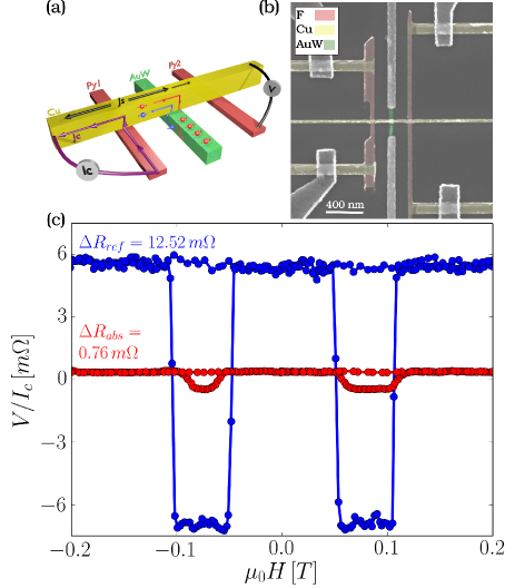
Figure 1 represents (a) a sketch and (b) a scanning electron microscope image of a typical device fabricated using the multi-angle nano-fabrication method (Laczkowski et al., 2011), where the colors red, yellow, and green represents ferromagnetic, non-magnetic and SHE material respectively. First, the middle wire is deposited on the substrate using Physical Vapor Deposition (PVD) and a lift-off technique, followed by the nano-fabrication of a lateral spin-valve. In between these two steps the middle wire surface is cleaned using Ar ion-milling. The Py, Cu and nano-wires are , and thick respectively. Their width is fixed to with an exception of the wide . The distance separating the ferro-magnets in the presented device is (from center to center of ferro-magnets).
Non-local measurements have been performed, using a standard Lock-in amplifier technique at , for two types of nano-structures. The first one as a reference is a regular non local device (Laczkowski et al., 2011) including a Cu channel and two ferromagnetic Py electrodes whereas the second one includes a wire inserted in between the ferromagnetic electrodes [Fig. 1(a-b)]. In these experiments a spin accumulation is created in the LSV by passing a partly spin-polarized charge current through a ferromagnetic/non-magnetic interface () [Fig. 1(a)]. The spin accumulation diffuses in both directions from this interface in Cu giving rise to spin currents. On the right-hand side of the LSV there are only pure spin currents without a net charge flow ( black arrows ) which are partially absorbed by the nano-wire. The voltage is measured across the second interface in order to probe spin currents arriving at this interface. The amplitude of the spin signal for reference and absorption devices was measured to be and respectively which yields an absorption of (independent of temperature) [Fig. 1(c)].
These experiments allow the experimental evaluation of the spin diffusion length of of AuW7% to be determined as long as the absorption ratio is known. The resistivity of the inserted material, , can be directly measured, however the spin diffusion length needs to be calculated. For the general case of the LSV, using a 1D model (Kimura, Hamrle, and Otani, 2005; Jaffres, George, and Fert, 2010), the ratio of the spin signal amplitude with the middle wire to the spin signal amplitude without this nano-wire equals 111Presented formula is a simplified version of the equation from (Kimura, Hamrle, and Otani, 2005).:
| (1) |
Here stands for spin resistances, where: , , , , , , are the resistivity, the spin diffusion length, the thickness, the width and the effective cross sectional area respectively. In the presented notation subscripts F and N correspond to the ferromagnetic and non-magnetic material respectively. The spin resistance of the inserted nano-wire is:
This allows for of the AuW nano-wire to be extracted knowing material characteristic parameters of the LSV: AuW resistivity and thickness . Remaining LSVs parameters are: , , and the characteristic spin transport parameters: and , which were taken from our previous experiments (Laczkowski, 2012; Rojas Sanchez et al., 2013; Motzko et al., 2013). These results are in agreement with what can be found in literature for similar structures (Bass and Pratt, 2007). This analysis leads to the spin diffusion length of to be .
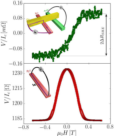
Moreover, one can also perform SHE experiments in the very same structure. A spin current is injected electrically by using interface as presented above. The spin current absorbed by the nano-wire is then converted into a transverse charge current via the SHE and thus leads to an electric voltage signal. The external magnetic field is swept along the non-magnetic Cu channel while a voltage drop is measured on the nano-wire edges.
Figure 2 shows experimental data-points obtained at for the Inverse-SHE when the voltage is measured at the edge of the AuW wire and Anisotropic Magneto-resistance (AMR) in 2 contacts at the edge of the Py injector. Probe configurations are represented schematically in corresponding insets. A clear non-local signal is observed yielding . Its amplitude is a roughly linear function of the magnetic field in a region below the saturation field which corresponds to the situation where the magnetization of the ferromagnetic injector (Py1) is fully parallel to the non-magnetic Cu channel.
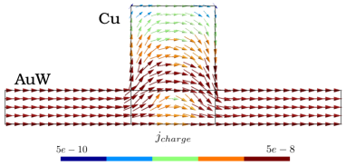
It is known that evaluating the spin Hall angle with a simple 1D model leads to underestimation of the due to the shunting effect (Niimi et al., 2011, 2012). We then performed a more sophisticated analysis using a Finite Element Method (FEM) simulation (Laczkowski, 2012). The result of this analysis shows that the spin Hall angle is larger than the one obtained with the 1D model () (Takahashi and Maekawa, 2008). Two effects contribute to underevaluation of the with the 1D model. The main effect is due to shunting by the Cu layer of a part of the ISHE current produced by the spin current absorption in AuW nano-wire. The current distribution is quite inhomogeneous and therefore one should take into account only a shunt by a part of the Cu layer in the same order of magnitude than about half the contact width. This leads to the 1D model correction factor of about 12 (related directly with the resistivity ratio). This can be view in figure 3 where 90% of the current extends on about in Cu layer. This emphasizes the 1D model limitation with these aspect ratios and the requirement to use a finite element model in order to analyze the data correctly. The second effect is linked to the spreading of the spin accumulation over the sides of the contacts in the SHE material mainly when the spin diffusion length of the SHE materials is long, compared to the width . In our case with a spin diffusion length of about compared to the thickness of , this effect should be negligible giving a posteriori justification of the derivation of the with 1D model [Eq. 1].
We turn now to the second experiment performed at room temperature: spin pumping and ISHE where the ferromagnetic resonance (FMR) is exploited. The resistivity variation from 10K up to 300K for AuW7% is , almost insensitive to temperature due to the dominant role of the scattering by impurities. We thus expect (as well as ) to be independent of the temperature and that the two measurement results can be directly compared. We have grown by sputtering a bilayer, and a reference sample. In a usual FMR experiment, a microwave is applied at a given frequency and power with a magnetic field strength . Additionally, a perpendicular magnetic field is swept. At the resonance condition, when is parallel to the film plane, a pure spin current is be injected from the Py layer to the layer. This is the spin pumping effect (Tserkovnyak, Brataas, and Halperin, 2005) which can be detected by the increase of the damping constant in the bilayer with respect to the single Py reference sample. Due to the ISHE in the layer, the injected spin current is converted into a charge current, which, in turn, can be detected as a transverse voltage.
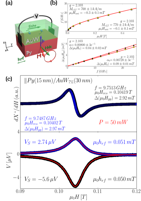
A typical schematic of the spin pumping-ISHE experiment is shown in Fig. 4(a). As described previously (Jain et al., 2012; Rojas-Sánchez et al., 2013) we have used a broadband stripe system to accurately determine the damping constant [Fig. 4(b)] and we have used an X-band cylindrical cavity to measure the FMR spectrum and the voltage due to the ISHE [Fig. 4(c)]. The frequency f vs. magnetic resonant field, , allows the effective magnetic saturation and in plane anisotropy to be calculated as displayed in Fig. 4(b) top. We can observe that both samples, the reference and the bilayer have the same value and a negligible in-plane magnetic anisotropy (). The linear frequency dependence of the peak-to-peak linewidth () allows extraction of the damping constant and the f-independent contribution , due to inhomogeneities. A linear behavior is found on both samples in the whole experimental range [Fig. 4(b) bottom]. Furthermore, the contribution due to inhomogeneities is very small, , and a small but clear increase of the damping constant for can be observed (with respect to the reference sample). Thus we can conclude, that the layer acts as a spin sink layer. This can be verified in the simultaneously measurement [Fig. 4(c)], where we can observe a symmetrical Lorentzian voltage peak at the resonance field.
In order to quantify the spin Hall angle of this material we use all our experimental values taking advantage of the spin diffusion length already determined in the previous section (which is invariant of temperature). The effective spin mixing conductivity is calculated as (Tserkovnyak, Brataas, and Halperin, 2005; Mosendz et al., 2010): , where F(N) stands for Py(AuW7%) layer, is the effective demagnetization field, is the Landé g-factor, is the Bohr constant, is , and all other values are shown in Fig. 4(b). The effective spin current density injected at the interface, while considering a transparent interface (no spin decoherence), is given by (Ando and Saitoh, 2010; Mosendz et al., 2010; Rojas-Sánchez et al., 2013):
| (2) |
where e is the electron charge, is the Dirac constant, and . Considering and , we obtain . In order to eliminate undesirable effects (Feng et al., 2012; Rojas-Sánchez et al., 2013) the transverse voltage amplitudes in between two magnetic field directions have been averaged and weighted by . We obtain a value of . Independently, we have measured the sheet resistance of the bilayer, , which gives the resistance of sized sample to be . Then the charge current weighted by is . The conversion between the spin current density and the charge current due to the ISHE is expressed by (Ando and Saitoh, 2010; Mosendz et al., 2010; Rojas-Sánchez et al., 2013):
| (3) |
where is the thickness of the layer and accounts for the spin flip scattering at the interface (Rojas-Sánchez et al., 2013). Considering transparent interface () and using the previous values one obtains a lower boundary for the spin Hall angle of , , where the “+” indicates the same SHE sign as in Pt. Interface spin resistance and spin memory loss parameters are not yet well known in , but the integration of such quantities will necessarily lead to an increase of the determined spin Hall angle (Rojas-Sánchez et al., 2013). At this point, we cannot state whether the extrinsic SHE is due to skew scattering or side jump. Additional experiments are in progress to elucidate this question. In this study we have also verified that for pure Au is around , which is close to the value reported elsewhere (Mosendz et al., 2010). Despite of the small damping enhancement, comparable with pure Au and Ta, we have estimated a large which makes this alloy attractive for applications which require a low damping constant.
In summary we have successfully developed a gold alloy with a heavy element in order to increase its spin Hall angle. We have shown by complementary studies, that the spin diffusion length of is and its spin Hall angle is at least %. This value is more than one order of magnitude higher than in a pure gold and can probably be further increased with higher impurity concentrations. The large spin Hall angle in makes this material very attractive for future developments of spintronics devices, which incorporate non magnetic materials in order to detect or to generate pure spin currents. In particular, its stability at room temperature and its chemical inertia are technologically advantageous compared to other materials. Future research should investigate the spin memory loss effect at the interface, to determine the dominant scattering mechanism and optimize the W concentration in order to maximize the spin/charge current conversion efficiency.
Acknowledgements.
We acknowledge U. Ebels, S. Gambarelli, and G. Desfonds for technical support with the FMR measurements. This Work was partly supported by the French Agence Nationale de la Recherche (ANR) through projects SPINHALL (2010-2013) and SOSPIN (2013-2016).References
- Dyakonov and Perel (1971) M. Dyakonov and V. Perel, Physics Letters A 35, 459 (1971).
- Hirsch (1999) J. E. Hirsch, Phys. Rev. Lett. 83, 1834 (1999).
- Inoue and Ohno (2005) J. Inoue and H. Ohno, Science 309, 2004 (2005).
- Saitoh et al. (2006) E. Saitoh, M. Ueda, H. Miyajima, and G. Tatara, Applied Physics Letters 88, 182509 (2006).
- Kimura et al. (2007) T. Kimura, Y. Otani, T. Sato, S. Takahashi, and S. Maekawa, Phys Rev Lett 98, 156601 (2007).
- Vila, Kimura, and Otani (2007) L. Vila, T. Kimura, and Y. Otani, Phys. Rev. Lett. 99, 226604 (2007).
- Liu, Buhrman, and Ralph (2011) L. Liu, R. Buhrman, and D. Ralph, arXiv preprint arXiv:1111.3702 (2011).
- Ando and Saitoh (2010) K. Ando and E. Saitoh, Journal of Applied Physics 108, 113925 (2010).
- Kato et al. (2004) Y. Kato, R. Myers, A. Gossard, and D. Awschalom, Science 306, 1910 (2004).
- Wunderlich et al. (2005) J. Wunderlich, B. Kaestner, J. Sinova, and T. Jungwirth, Physical review letters 94, 047204 (2005).
- Liu et al. (2012) L. Liu, C.-F. Pai, Y. Li, H. Tseng, D. Ralph, and R. Buhrman, Science 336, 555 (2012).
- Niimi et al. (2013) Y. Niimi, D. Wei, H. Idzuchi, T. Wakamura, T. Kato, and Y. Otani, Physical Review Letters 110, 016805 (2013).
- Miron et al. (2011) I. M. Miron, K. Garello, G. Gaudin, P.-J. Zermatten, M. V. Costache, S. Auffret, S. Bandiera, B. Rodmacq, A. Schuhl, and P. Gambardella, Nature 476, 189 (2011).
- Liu et al. (2011) L. Liu, T. Moriyama, D. C. Ralph, R. A. Buhrman, and M. T. R. D. C. B. R. A, Physical Review Letters 106, 36601 (2011).
- Pershin et al. (2009) Y. V. Pershin, N. A. Sinitsyn, A. Kogan, A. Saxena, and D. L. Smith, Applied Physics Letters 95, 022114 (2009).
- Wunderlich et al. (2010) J. Wunderlich, B.-G. Park, A. C. Irvine, L. P. Zârbo, E. Rozkotová, P. Nemec, V. Novák, J. Sinova, and T. Jungwirth, Science 330, 1801 (2010).
- Bauer, Saitoh, and van Wees (2012) G. E. Bauer, E. Saitoh, and B. J. van Wees, Nature materials 11, 391 (2012).
- Tanaka et al. (2008) T. Tanaka, H. Kontani, M. Naito, T. Naito, D. S. Hirashima, K. Yamada, and J. Inoue, Phys. Rev. B 77, 165117 (2008).
- Kontani et al. (2009) H. Kontani, T. Tanaka, D. S. Hirashima, K. Yamada, and J. Inoue, Phys. Rev. Lett. 102, 016601 (2009).
- Morota et al. (2011) M. Morota, Y. Niimi, K. Ohnishi, D. H. Wei, T. Tanaka, H. Kontani, T. Kimura, and Y. Otani, Phys. Rev. B 83, 174405 (2011).
- Smit (1958) J. Smit, Physica 24, 39 (1958).
- Berger (1970) L. Berger, Physical Review B (1970).
- Fert, Friederich, and Hamzic (1981) A. Fert, A. Friederich, and A. Hamzic, Journal of Magnetism and Magnetic Materials 24, 231 (1981).
- Fert and Levy (2011) A. Fert and P. M. Levy, Physical review letters 106, 157208 (2011).
- Niimi et al. (2011) Y. Niimi, M. Morota, D. H. Wei, C. Deranlot, M. Basletić, A. Hamzić, a. Fert, and Y. Otani, Physical Review Letters 106, 126601 (2011).
- Niimi et al. (2012) Y. Niimi, Y. Kawanishi, D. H. Wei, C. Deranlot, H. X. Yang, M. Chshiev, T. Valet, A. Fert, and Y. Otani, Phys. Rev. Lett. 109, 156602 (2012).
- Niimi et al. (2014) Y. Niimi, H. Suzuki, Y. Kawanishi, Y. Omori, T. Valet, A. Fert, and Y. Otani, Phys. Rev. B 89, 054401 (2014).
- Yamanouchi et al. (2013) M. Yamanouchi, L. Chen, J. Kim, M. Hayashi, H. Sato, S. Fukami, S. Ikeda, F. Matsukura, and H. Ohno, Applied Physics Letters 102, 212408 (2013).
- Datta, Salahuddin, and Behin-Aein (2012) S. Datta, S. Salahuddin, and B. Behin-Aein, Applied Physics Letters 101, 252411 (2012).
- Manipatruni, Nikonov, and Young (2013) S. Manipatruni, D. Nikonov, and I. Young, arXiv preprint arXiv:1301.5374 , 1 (2013).
- Kimura, Hamrle, and Otani (2005) T. Kimura, J. Hamrle, and Y. Otani, Phys. Rev. B 72, 014461 (2005).
- Laczkowski et al. (2011) P. Laczkowski, L. Vila, S. Ferry, A. Marty, J.-M. George, H. Jaffrès, A. Fert, T. Kimura, T. Yang, Y. Otani, and J.-P. Attané, Applied Physics Express 4, 1 (2011).
- Jaffres, George, and Fert (2010) H. Jaffres, J.-M. George, and A. Fert, Phys. Rev. B 82, 140408 (2010).
- Note (1) Presented formula is a simplified version of the equation from (Kimura, Hamrle, and Otani, 2005).
- Laczkowski (2012) P. Laczkowski, Courants de spin et l’effet Hall de spin dans des nanostructures latérales, Ph.D. thesis, Grenoble (2012).
- Rojas Sanchez et al. (2013) J.-C. Rojas Sanchez, P. Laczkowski, W. Savero Torres, M. Cubukcu, V. Nguyen, L. Notin, C. Beigné, C. Vergnaud, A. Marty, M. Jamet, et al., Applied Physics Letters 102, 132408 (2013).
- Motzko et al. (2013) N. Motzko, B. Burkhardt, N. Richter, R. Reeve, P. Laczkowski, W. S. Torres, L. Vila, J.-P. Attané, and M. Kläui, Physical Review B 88, 214405 (2013).
- Bass and Pratt (2007) J. Bass and W. P. Pratt, Journal of Physics: Condensed Matter 19, 183201 (2007).
- Takahashi and Maekawa (2008) S. Takahashi and S. Maekawa, Science and Technology of Advanced Materials 9, 014105 (2008).
- Tserkovnyak, Brataas, and Halperin (2005) Y. Tserkovnyak, A. Brataas, and B. I. Halperin, Reviews of Modern Physics 77, 1375 (2005).
- Jain et al. (2012) A. Jain, J.-C. Rojas-Sanchez, M. Cubukcu, J. Peiro, J. Le Breton, E. Prestat, C. Vergnaud, L. Louahadj, C. Portemont, C. Ducruet, et al., Physical review letters 109, 106603 (2012).
- Rojas-Sánchez et al. (2013) J.-C. Rojas-Sánchez, M. Cubukcu, A. Jain, C. Vergnaud, C. Portemont, C. Ducruet, A. Barski, A. Marty, L. Vila, J.-P. Attané, E. Augendre, G. Desfonds, S. Gambarelli, H. Jaffrès, J.-M. George, and M. Jamet, Phys. Rev. B 88, 064403 (2013).
- Mosendz et al. (2010) O. Mosendz, V. Vlaminck, J. E. Pearson, F. Y. Fradin, G. E. W. Bauer, S. D. Bader, and A. Hoffmann, Physical Review B 82, 214403 (2010).
- Rojas-Sánchez et al. (2013) J.-C. Rojas-Sánchez, N. Reyren, P. Laczkowski, W. Savero, J.-P. Attané, C. Deranlot, M. Jamet, J.-M. George, L. Vila, and H. Jaffrès, arXiv preprint arXiv:1312.2717 (2013).
- Feng et al. (2012) Z. Feng, J. Hu, L. Sun, B. You, D. Wu, J. Du, W. Zhang, a. Hu, Y. Yang, D. M. Tang, B. S. Zhang, and H. F. Ding, Physical Review B 85, 214423 (2012).