Semiconducting-to-metallic photoconductivity crossover and temperature-dependent Drude weight in graphene
Abstract
We investigated the transient photoconductivity of graphene at various gate-tuned carrier densities by optical-pump terahertz-probe spectroscopy. We demonstrated that graphene exhibits semiconducting positive photoconductivity near zero carrier density, which crosses over to metallic negative photoconductivity at high carrier density. Our observations are accounted for by considering the interplay between photo-induced changes of both the Drude weight and the carrier scattering rate. Notably, we observed multiple sign changes in the temporal photoconductivity dynamics at low carrier density. This behavior reflects the non-monotonic temperature dependence of the Drude weight, a unique property of massless Dirac fermions.
Charge carriers in graphene mimic two-dimensional massless Dirac fermions with linear energy dispersion, resulting in unique optical and electronic properties Castro Neto et al. (2009); *DasSarma2011. They exhibit high mobility and strong interaction with electromagnetic radiation over a broad frequency range Mak et al. (2012). Interband transitions in graphene give rise to pronounced optical absorption in the mid-infrared to visible spectral range, where the optical conductivity is close to a universal value (Ref. Mak et al., 2008; *Li2008; *Wang2008). Free-carrier intraband transitions, on the other hand, give rise to low-frequency absorption, which varies significantly with charge density and can cause strong extinction of light in the high density limit Horng et al. (2011); *Ren2012. In addition to this density dependence, the massless Dirac particles in graphene are predicted to exhibit a distinctive non-monotonic temperature dependence of the intraband absorption strength, or Drude weight, due to their linear dispersion Müller et al. (2009); Gusynin et al. (2009). This behavior contrasts with the temperature-independent Drude weight expected in conventional systems of massive particles with parabolic dispersion Gusynin et al. (2007). While the unique behavior of the Drude weight in graphene has been considered theoretically, a clear experimental signature is still lacking.
The intrinsic properties of Drude absorption in graphene can be revealed by studying its dynamical response to photoexcitation. In particular, optical-pump terahertz-probe spectroscopy provides access to a wide transient temperature range via pulsed optical excitation, and allows measurement of the dynamical Drude conductivity by a time-delayed terahertz (THz) probe pulse Ulbricht et al. (2011). This technique has been applied to study transient photoconductivity in graphene, but conflicting results have been reported Kampfrath et al. (2005); Jnawali et al. (2013); Frenzel et al. (2013); Docherty et al. (2012); Tielrooij et al. (2013); Choi et al. (2009); *Strait2011; *Winnerl2011; *Kim2013b. Positive photoconductivity was observed in epitaxial graphene on SiC (Ref. Choi et al., 2009), while negative photoconductivity was seen in graphene grown by chemical vapor deposition (CVD; Refs. Jnawali et al., 2013; Frenzel et al., 2013; Docherty et al., 2012; Tielrooij et al., 2013). The opposite behavior in these samples has been argued to arise from their different charge densities. Gate tunable carrier density in a single sample promises to resolve these conflicts and allow observation of unique Dirac fermion behavior.
In this Letter, we present an investigation of the Drude absorption dynamics in graphene over a wide range of carrier density and temperature. Using optical-pump THz-probe spectroscopy, we drove the carriers to high transient temperature and probed the Drude absorption of the hot carriers as they relaxed to equilibrium. By adjusting the pump-probe delay, we were able to observe the change of Drude absorption over a broad range of transient temperature. At low charge density, we observed complicated temporal dynamics of the THz Drude response, where the sign of photoconductivity changed multiple times as the carrier temperature increased and decreased. This is a signature of the non-monotonic temperature dependence of the Drude weight in graphene, an intrinsic characteristic of massless Dirac fermions. Additionally, we observed the carrier-density dependence of the dynamical Drude response through electrostatic gating of our samples. Near the charge neutrality point, our samples exhibited positive (semiconductor) photoconductivity, due to thermally excited electron-hole pairs after photoexcitation. At high charge density, however, graphene exhibited negative (metallic) photoconductivity because of an optically-induced decrease of the Drude weight, coupled with increased carrier scattering rate. The observed density-dependent photoconductivity provides a unifying framework for understanding previously reported positive photoconductivity in (undoped) epitaxial graphene and negative photoconductivity in (-doped) CVD graphene. By using the Drude model with an estimated temporal evolution of the hot carrier temperature, we were able to reproduce all the main features of our observations.
A key advance in our experiment is the fabrication of large-area gated graphene devices without a THz photoconductivity response from the substrate [Fig. 1(a)]. This is not possible for commonly used SiO2/Si substrates, which produce large background signal in optical-pump THz-probe experiments Suzuki and Shimano (2011). Here, we used -cut crystalline quartz substrates and deposited 35-nm indium tin oxide (ITO) and 400-nm parylene-C thin films as the back gate electrode and dielectric, respectively. We experimentally confirmed that the back-gate structure had negligible pump-probe response (see Supplemental Material online, Ref. SOM, ). High-quality single-layer CVD graphene Li et al. (2009) sheets were transferred to our back-gate substrates. Graphite-paint source and drain electrodes were attached to graphene with a separation of 5 mm. The devices exhibited excellent bipolar gating behavior with low unintentional doping [Fig. 1(b); gate voltage V at charge neutrality, corresponding to cm-2, estimated from our device capacitance].
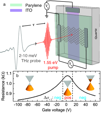
The graphene devices, investigated at room temperature in high vacuum ( Torr), were optically excited with 100 fs laser pulses at 1.55 eV photon energy generated using a 5 kHz amplified Ti:sapphire laser system. The transient photoconductivity was probed by measuring the complex transmission coefficient of picosecond THz pulses (photon energy 2-10 meV) with controllable time delay [Fig. 1(a)]. To reduce experimental errors associated with laser drift, we simultaneously measured the electric field waveform of the THz pulse transmitted through the sample in equilibrium and the optical pump-induced change of the transmitted field via electro-optic sampling Werley et al. (2011); SOM . In our experiments, the ratio (referred to as “differential field”) approximately represents the photoconductivity (Refs. Kampfrath et al., 2005; Jnawali et al., 2013; Frenzel et al., 2013; SOM, ).
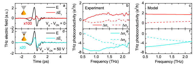
Pump-probe measurements with incident pump fluence J/cm2 and pump-probe delay ps reveal that the sign of the photoconductivity can be tuned from positive at charge neutrality to negative at a moderate carrier density [Fig. 2]. The measured at charge neutrality () in panel (a) is everywhere opposite in sign to , reflecting a photo-induced increase in absorption. The photoconductivity , calculated from the waveforms in (a) and taking the device geometry into account, shows a positive real part [Fig. 2(b)]. In sharp contrast, has the same profile and sign as when V ( cm-2), implying a photo-induced decrease in absorption [Fig. 2(d)]. As expected, the absorptive part of the photoconductivity, , is negative in this case [Fig. 2(e)].
To further investigate the mechanism driving the observed crossover, we measured the temporal dynamics of at various carrier densities. Fig. 3(a) displays the ratio at fixed [Figs. 2(a,d)] for gate voltages between -100 V and +50 V from . The relaxation time of the signal was approximately 2 ps, with no systematic dependence on carrier density. To more directly show the carrier density dependence, we plot the average value of the differential field, , as a function of gate voltage in Fig. 3(c). These data show that the overall photoconductivity signal quickly changes from positive at charge neutrality to negative at moderate charge density.

The opposite sign of observed in graphene at the limits of charge neutrality and high charge density can be qualitatively understood by considering the interplay between photo-induced changes of carrier population and scattering rate (The more complicated behavior at low charge density is addressed in detail below). Photoexcited carriers in graphene are known to thermalize rapidly within a few 10s of fs Lui et al. (2010); *Breusing2011; *Brida2013; *Johannsen2013; *Gierz2013. Therefore, due to the 100 fs temporal resolution in our experiment, the charge carriers can be well described by a thermal distribution at temperature for all pump-probe delay times . For graphene near the charge neutrality point, an increase of carrier temperature promotes the free-carrier population and thus enhances absorption. Such behavior mimics that observed in epitaxial graphene Choi et al. (2009); Strait et al. (2011) and other semiconductors Ulbricht et al. (2011), where the optically generated electron-hole pairs increase the infrared absorption. For graphene with high carrier density, laser-induced carrier heating only modifies the carrier distribution near the Fermi level, without changing the total carrier density. The carrier scattering rate, however, increases due to an enlarged phase space for scattering and the presence of hot optical phonons after optical excitation. This causes a reduction of free-carrier absorption, a behavior analogous to that in metals and observed in -doped CVD graphene Tielrooij et al. (2013); Frenzel et al. (2013); Docherty et al. (2012); Jnawali et al. (2013).
For a more thorough and quantitative analysis at all charge densities, we consider the Drude model for free carrier conductivity in graphene Gusynin et al. (2009); Horng et al. (2011); Strait et al. (2011); Frenzel et al. (2013); Jnawali et al. (2013),
| (1) |
Here, is the transport scattering rate and is the Drude weight, which quantifies the oscillator strength of free-carrier absorption. In a metal or semiconductor with parabolic dispersion, , independent of temperature SOM . In graphene and other 2D systems with linear dispersion, however, exhibits a distinctive carrier temperature dependence Gusynin et al. (2009); Müller et al. (2009); Wagner et al. (2014); SOM :
| (2) |
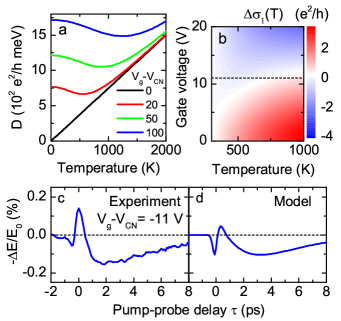
Fig. 4(a) shows that increases linearly with temperature when , and approaches for electronic temperatures .
While only depends on the electron temperature , the transport scattering rate depends on , , and the phonon temperature differently for different scattering mechanisms Hwang and Das Sarma (2008); *Fratini2008; *Hwang2009. Optical excitation can therefore alter the THz conductivity [Eq. (1)] through the dependence of and on and . In our sample, we expect that charged impurities and hot optical phonons dominate the scattering rate Perebeinos and Avouris (2010); Hwang and Das Sarma (2008); Malard et al. (2013); SOM . We calculated the temperature- and density-dependent change in conductivity relevant to our experiment, K), at representative frequency THz, as shown in Fig. 4(b). For this calculation, we assumed that (Refs. Kampfrath et al., 2005; Lui et al., 2010). The color plot shows that is positive (red area) near charge neutrality ( V), but becomes negative (blue area) at high carrier density ( V), as anticipated from the qualitative discussion above.
We can convert the calculated to photoconductivity by considering the temperature dynamics in graphene following photoexcitation. We estimated the transient temperature by comparison with previous publications Lui et al. (2010); Malard et al. (2013); Graham et al. (2013) and simulated the temporal photoconductivity dynamics. The time-dependent temperature was assumed to consist of two exponential decays with time constants ps and ps and a 200 fs rise time Malard et al. (2013); Graham et al. (2013). The maximum estimated temperature was 500 K for 3 J/cm2 incident fluence and 800 K for 10 J/cm2 (Ref. SOM, ). Our simulated photoconductivity spectra, shown in Figs. 2(c,f), capture the main features of the experimental data [Figs. 2(a,d)]. Based on these spectra, we also calculated the expected , shown in Figs. 3(b,d). The good agreement between experiment and simulation demonstrates that our model correctly captures the relevant physics of transient photoconductivity in graphene.
We gain further insight into the transient photoconductivity dynamics in graphene by examining the transition regime between positive and negative photoconductivity [Fig. 4(c)]. The complicated temporal dynamics, characterized by multiple sign changes on a picosecond timescale, are due to the non-monotonic temperature dependence of the Drude weight. In graphene with finite carrier density, the Drude weight [Fig. 4(a)] initially drops as temperature increases, reaches a minimum at , then increases linearly at higher temperature Müller et al. (2009); SOM . Correspondingly, at intermediate carrier density is initially negative, then becomes positive as temperature increases [dashed line in Fig. 4(b)]. In our pump-probe experiment, the optical pump pulse initially heats the carriers to high temperature, resulting in a sign change of from negative to positive. As the carriers then cool, changes sign to negative again before returning to zero at equilibrium. Our observed temporal photoconductivity dynamics [Fig. 4(c)], which follow this sequence of sign changes, explicitly reveal the non-monotonic temperature-dependence of the Drude weight in graphene. Using the same parameters as before, our model reproduces this behavior [Fig. 4(d)]. We note that these temporal dynamics do not appear in our simulation if we neglect the non-monotonic temperature dependence of (Ref. SOM, ).
The unusual non-monotonic temperature dependence of the Drude weight can be understood by considering the conservation of spectral weight of optical transitions Kuzmenko et al. (2008); Gusynin et al. (2009); Horng et al. (2011). The optical absorption spectrum in graphene consists of two contributions: high-energy interband absorption and low-energy intraband absorption. Interband absorption in graphene with finite charge density shows an onset at photon energy due to Pauli blocking Mak et al. (2008); Gusynin et al. (2009); Horng et al. (2011). When carriers are heated to moderate temperatures , decreases due to particle conservation Ashcroft and Mermin (1976). This decreases the interband absorption threshold, increasing the interband spectral weight. To conserve total spectral weight, the intraband absorption must therefore decrease. When carrier temperatures become comparable to , however, interband transitions are Pauli blocked by thermally excited carriers, reducing the spectral weight. This increases the intraband spectral weight, as has been observed in graphite Kuzmenko et al. (2008). We emphasize that this behavior is due to the linear dispersion of charge carriers in graphene, and is absent in materials with parabolic dispersion.
In conclusion, we have studied the temperature- and density-dependent Drude conductivity in graphene through its dynamical response to pulsed photoexcitation. We demonstrated that the transient photoconductivity behavior of graphene can be tuned continuously from semiconducting to metallic by varying the Fermi level from the charge neutrality point to either the electron or hole side. This resolves the controversy between previous experiments which observed positive photoconductivity in epitaxial graphene and negative photoconductivity in CVD graphene. By detailed simulation based on the Drude model, we found that photo-induced changes of both Drude weight and carrier scattering rate play important roles in the THz photoconductivity dynamics. In particular, complicated temporal evolution of the photoconductivity at low charge density serves as a direct signature of the non-monotonic temperature dependence of the Drude weight in graphene, a unique property of systems with linear energy dispersion.
Note: upon completion of this work, we became aware of similar work by another group Shi et al. (2014).
Acknowledgements.
The authors acknowledge helpful discussions with J.C.W. Song and O. Khatib, and thank V. Fatemi, J.D. Sanchez-Yamagishi, and M.A. Smith for assistance with device fabrication. This work was supported by Department of Energy Office of Basic Energy Sciences Grant No. DE-SC0006423 (sample fabrication, experimental setup, and data acquisition) and STC Center for Integrated Quantum Materials, NSF grant DMR-1231319 (data analysis). A.J.F. acknowledges support from NSF GRFP. This work also made use of Harvard’s Center for Nanoscale Systems (CNS), supported by the National Science Foundation under grant No. ECS-0335765, and the MIT Microsystems Technology Laboratory (MTL).References
- Castro Neto et al. (2009) A. H. Castro Neto, N. M. R. Peres, K. S. Novoselov, and A. K. Geim, Rev. of Mod. Phys. 81, 109 (2009).
- Das Sarma et al. (2011) S. Das Sarma, S. Adam, E. H. Hwang, and E. Rossi, Rev. of Mod. Phys. 83, 407 (2011).
- Mak et al. (2012) K. F. Mak, L. Ju, F. Wang, and T. F. Heinz, Solid State Comm. 152, 1341 (2012).
- Mak et al. (2008) K. F. Mak, M. Y. Sfeir, Y. Wu, C. H. Lui, J. A. Misewich, and T. F. Heinz, Phys. Rev. Lett. 101, 196405 (2008).
- Li et al. (2008) Z. Q. Li, E. A. Henriksen, Z. Jiang, Z. Hao, M. C. Martin, P. Kim, H. L. Stormer, and D. N. Basov, Nat. Phys. 4, 532 (2008).
- Wang et al. (2008) F. Wang, Y. Zhang, C. Tian, C. Girit, A. Zettl, M. Crommie, and Y. R. Shen, Science 320, 206 (2008).
- Horng et al. (2011) J. Horng, C.-F. Chen, B. Geng, C. Girit, Y. Zhang, Z. Hao, H. A. Bechtel, M. Martin, A. Zettl, M. F. Crommie, Y. R. Shen, and F. Wang, Phys. Rev. B 83, 165113 (2011).
- Ren et al. (2012) L. Ren, Q. Zhang, J. Yao, Z. Sun, R. Kaneko, Z. Yan, S. Nanot, Z. Jin, I. Kawayama, M. Tonouchi, J. M. Tour, and J. Kono, Nano Lett. 12, 3711 (2012).
- Müller et al. (2009) M. Müller, M. Bräuninger, and B. Trauzettel, Phys. Rev. Lett. 103, 196801 (2009).
- Gusynin et al. (2009) V. P. Gusynin, S. G. Sharapov, and J. P. Carbotte, New J. Phys. 11, 095013 (2009).
- Gusynin et al. (2007) V. Gusynin, S. Sharapov, and J. Carbotte, Phys. Rev. B 75, 165407 (2007).
- Ulbricht et al. (2011) R. Ulbricht, E. Hendry, J. Shan, T. Heinz, and M. Bonn, Rev. of Mod. Phys. 83, 543 (2011).
- Kampfrath et al. (2005) T. Kampfrath, L. Perfetti, F. Schapper, C. Frischkorn, and M. Wolf, Phys. Rev. Lett. 95, 187403 (2005).
- Jnawali et al. (2013) G. Jnawali, Y. Rao, H. Yan, and T. F. Heinz, Nano Lett. 13, 524 (2013).
- Frenzel et al. (2013) A. J. Frenzel, C. H. Lui, W. Fang, N. L. Nair, P. K. Herring, P. Jarillo-Herrero, J. Kong, and N. Gedik, Appl. Phys. Lett. 102, 113111 (2013).
- Docherty et al. (2012) C. J. Docherty, C.-T. Lin, H. J. Joyce, R. J. Nicholas, L. M. Herz, L.-J. Li, and M. B. Johnston, Nat. Comm. 3, 1228 (2012).
- Tielrooij et al. (2013) K. J. Tielrooij, J. C. W. Song, S. A. Jensen, A. Centeno, A. Pesquera, A. Zurutuza Elorza, M. Bonn, L. S. Levitov, and F. H. L. Koppens, Nat. Phys. 9, 248 (2013).
- Choi et al. (2009) H. Choi, F. Borondics, D. A. Siegel, S. Y. Zhou, M. C. Martin, A. Lanzara, and R. A. Kaindl, Appl. Phys. Lett. 94, 172102 (2009).
- Strait et al. (2011) J. H. Strait, H. Wang, S. Shivaraman, V. Shields, M. Spencer, and F. Rana, Nano Lett. 11, 4902 (2011).
- Winnerl et al. (2011) S. Winnerl, M. Orlita, P. Plochocka, P. Kossacki, M. Potemski, T. Winzer, E. Malic, A. Knorr, M. Sprinkle, C. Berger, W. de Heer, H. Schneider, and M. Helm, Phys. Rev. Lett. 107, 237401 (2011).
- Kim et al. (2013) J. Kim, S. C. Lim, S. J. Chae, I. Maeng, Y. Choi, S. Cha, Y. H. Lee, and H. Choi, Scientific Reports 3, 2663 (2013).
- Suzuki and Shimano (2011) T. Suzuki and R. Shimano, Phys. Rev. B 83, 085207 (2011).
- (23) See Supplemental Material online for more information .
- Li et al. (2009) X. Li, W. Cai, J. An, S. Kim, J. Nah, D. Yang, R. Piner, A. Velamakanni, I. Jung, E. Tutuc, S. K. Banerjee, L. Colombo, and R. S. Ruoff, Science 324, 1312 (2009).
- Werley et al. (2011) C. A. Werley, S. M. Teo, and K. A. Nelson, Rev. Sci. Inst. 82, 123108 (2011).
- Lui et al. (2010) C. H. Lui, K. F. Mak, J. Shan, and T. Heinz, Phys. Rev. Lett. 105, 127404 (2010).
- Breusing et al. (2011) M. Breusing, S. Kuehn, T. Winzer, E. Malić, F. Milde, N. Severin, J. P. Rabe, C. Ropers, A. Knorr, and T. Elsaesser, Phys. Rev. B 83, 153410 (2011).
- Brida et al. (2013) D. Brida, A. Tomadin, C. Manzoni, Y. J. Kim, A. Lombardo, S. Milana, R. R. Nair, K. S. Novoselov, A. C. Ferrari, G. Cerullo, and M. Polini, Nat. Comm. 4, 1987 (2013).
- Johannsen et al. (2013) J. C. Johannsen, S. Ulstrup, F. Cilento, A. Crepaldi, M. Zacchigna, C. Cacho, I. C. E. Turcu, E. Springate, F. Fromm, C. Raidel, T. Seyller, F. Parmigiani, M. Grioni, and P. Hofmann, Phys. Rev. Lett. 111, 027403 (2013).
- Gierz et al. (2013) I. Gierz, J. C. Petersen, M. Mitrano, C. Cacho, I. C. E. Turcu, E. Springate, A. Stöhr, A. Köhler, U. Starke, and A. Cavalleri, Nat. Mater. 12, 1119 (2013).
- Wagner et al. (2014) M. Wagner, Z. Fei, A. S. McLeod, A. S. Rodin, W. Bao, E. G. Iwinski, Z. Zhao, M. Goldflam, M. Liu, G. Dominguez, M. Thiemens, M. M. Fogler, A. H. Castro Neto, C. N. Lau, S. Amarie, F. Keilmann, and D. N. Basov, Nano Lett. (2014), 10.1021/nl4042577.
- Hwang and Das Sarma (2008) E. Hwang and S. Das Sarma, Phys. Rev. B 77, 115449 (2008).
- Fratini and Guinea (2008) S. Fratini and F. Guinea, Phys. Rev. B 77, 195415 (2008).
- Hwang and Das Sarma (2009) E. Hwang and S. Das Sarma, Phys. Rev. B 79, 165404 (2009).
- Perebeinos and Avouris (2010) V. Perebeinos and P. Avouris, Phys. Rev. B 81, 195442 (2010).
- Malard et al. (2013) L. M. Malard, K. Fai Mak, A. H. Castro Neto, N. M. R. Peres, and T. F. Heinz, New J. Phys. 15, 015009 (2013).
- Graham et al. (2013) M. W. Graham, S.-F. Shi, Z. Wang, D. C. Ralph, J. Park, and P. L. McEuen, Nano Lett. 13, 5497 (2013).
- Kuzmenko et al. (2008) A. Kuzmenko, E. van Heumen, F. Carbone, and D. van der Marel, Phys. Rev. Lett. 100, 117401 (2008).
- Ashcroft and Mermin (1976) N. W. Ashcroft and N. D. Mermin, Solid State Physics (Brooks Cole, 1976).
- Shi et al. (2014) S.-F. Shi, T.-T. Tang, B. Zeng, L. Ju, Q. Zhou, A. Zettl, and F. Wang, Nano Lett. (2014), 10.1021/nl404826r.