The emergence of topologically protected surface states in epitaxial Bi(111) thin films
Abstract
Quantum transport measurements including the Altshuler-Aronov-Spivak (AAS) and Aharonov-Bohm (AB) effects, universal conductance fluctuations (UCF), and weak anti-localization (WAL) have been carried out on epitaxial Bi thin films ( bilayers) on Si(111). The results show that while the film interior is insulating all six surfaces of the Bi thin films are robustly metallic. We propose that these properties are the manifestation of a novel phenomenon, namely, a topologically trivial bulk system can become topologically non-trivial when it is made into a thin film. We stress that what’s observed here is entirely different from the predicted 2D topological insulating state in a single bilayer Bi where only the four side surfaces should possess topologically protected gapless states.
pacs:
73.20-r, 73.25.+i, 73.50.-hHistorically Bi is a material where many interesting condensed matter phenomena were (first) observed. This includes the de Haas-van Alphen effect de Haase and van Alphen (1930), quantum size confinement effect Ogrin et al. (1966), quantum linear magnetoresistance Abrikosov. (2000), peculiar superconductivity Buckel and Hilsch (1954), and possibly fractional quantum Hall effect Behnia et al. (2007). Despite of decades of studies, many fundamental properties of Bi remain poorly understood. For example, the Bi surfaces conduct much better than the bulk Hofmann (2006). Even more dramatically, the surface of Bi remains metallic after the bulk is turned into insulating by reducing the thickness of Bi films Xiao et al. (2012).
The last phenomenon is reminiscent to the behavior of topological insulators. Given that many Bi-based compounds (e.g., BixSb1-x, Bi2Se3, Bi2Te3) are topological insulators Hasan and Kane (2010); Qi and Zhang (2011), “can reduction of thickness turn the Bi thin film into topological insulator from its topologically trivial bulk ?” This is the question we address in this letter. In the following we report the results of a number of quantum transport measurements and theoretical calculations. Combining these investigations we arrive at the the conclusion that Bi thin films are interesting examples where a topologically trivial system becomes non-trivial solely due to the reduction of thickness. Throughout this letter we focus on epitaxial Bi thin films grown on Si(111) substrate.
Polished single crystal semi-insulating Si(111) substrates with high resistivity ( cm at 250 K) were chemically cleaned before put into the ultrahigh vacuum (UHV) chamber. It is further flashed to 1300 K to obtain a well-ordered () reconstructed surface, on which the epitaxial growth of Bi is carried out at 300 K Nagao et al. (2004). The details of our experimental set-up can be found in Ref Tian et al. (2005); Yin et al. (2006); Xiao et al. (2012); Tian et al. (2009). A representative reflection high energy electron diffraction (RHEED) pattern of our MBE grown thin films is given in the inset of Fig. 1(a). Both large angle and grazing angle x-ray diffraction measurements confirm that the Bi films investigated in this work are fully strain released with bulk lattice constants. Before the film is taken out of the UHV chamber we cap it with 5 nm MgO to protect it from oxidation. The transport measurements were carried out in an Oxford Cryofree magnet system with temperature down to 1.4 K and magnetic field up to 9 T.
Fig. 1(a) plots the longitudinal resistivity versus temperature. Two characteristic behaviors are observed: a low temperature metallic behavior () and a higher temperature insulating behavior (). This result is consistent with the behavior of a thin film with an insulating interior but a metallic surface Xiao et al. (2012). More specifically we attribute the linearly rising resistivity at low temperatures to the transport behavior of the metallic surface (it is similar to the resistivity behavior of a monolayer indium film Matsuda et al. (2007)). In contrast we attribute the high temperature behavior to the conduction due to thermally activated (across the interior energy gap) electrons and holes. Additional support of the low temperature conduction being due to the surface states comes from the fact that the low temperature total conductance of Bi films grown on two different substrates stays constant for thickness in the range of 15-27.5 nm. To our knowledge, due to the presence of bulk carriers, none of the as grown topological insulators BixSb1-x, Bi2Se3, and Bi2Te3 has exhibited the insulating to metallic crossover as shown in Fig. 1(a).
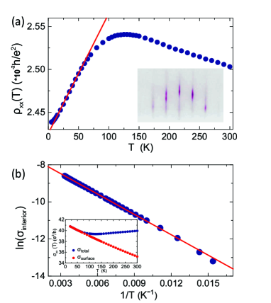
To separate the surface and interior conduction we first fit the linearly increasing resistivity by as marked by the red line in Fig. 1(a). The corresponding surface conductivity is shown in the inset of Fig. 1(b). By subtracting it from the total conductivity we obtain the temperature dependent conductivity of the film interior . In Fig.1(b) we plot versus . The slope gives an estimate of the interior energy gap. The result of this estimate is 62 meV. Our own angle resolved photoemission spectroscopic (ARPES) data on a 30 nm (75 BL) Bi(111) film confirms the existence of an indirect energy gap in the film interiorYao and Qian . Due to the 62 meV gap the low temperature transport discussed below is completely dominated by the surface conduction.
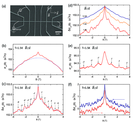
Next we demonstrate all six (top, bottom and four side) surfaces of the film are metallic. Fig. 2(a) shows a scanning electron microscope (SEM) picture of our device, in which both the current and magnetic field are applied along the x direction. The four probe method is used to measure the electric conductance. Fig. 2(b) shows the raw conductance versus magnetic field data for a 16 nm Bi film at T=1.5 K . Besides the weak anti-localization peak around zero magnetic field reproducible fine structures are observed on top of a smooth background (marked by the dashed line). After a background subtraction, quasi-periodic oscillations with a magnetic field period 0.55 T are clearly identified (see Fig. 2(c)). We attribute such oscillation to the Altshuler-Aronov-Spivak (AAS) oscillation Al’tshuler B. L. (1981). Using as the magnetic flux period, the above mentioned 0.55 T magnetic field period corresponds to a cross-section area of , which is in excellent agreement with the measured cross-section area ( and are the width and the thickness of the film). As usual the amplitudes of the AAS oscillations decreases with increasing the temperature (see Fig. 2(d)). In addition, as expected, for films with the same width and length but thinner thickness (8 nm film) the Aharonov-Bohm (AB) oscillation becomes more prominent (see Fig. 2(e)). The observation of the AAS and/or AB effect attests for the fact that the films under study have an insulating interior but a metallic surface. In particular, in order for the threaded flux to affect transport not only the top and the bottom but also the side surfaces need to be metallic. These metallic surface states are apparently very robust as they survived the “brutal” e-beam lithography.
Besides the AB and AAS oscillations, a careful examination of Fig. 2(c) reveals other finer structures (e.g., the features between peaks -5 and -6, and 2 and 3). We attribute them to the universal conductance fluctuations (UCF) Lee et al. (1987). Fig. 2(f) shows a couple of magneto-conductance curves (with the magnetic field applied perpendicular to the Bi film) after background subtraction. For the red trace the magnetic field sweeps from -4 to 4 T, while for the blue trace the magnetic field is reversed (see the arrows). All the fine structures in Fig. 2(f) (with the fluctuation amplitude ) are completely reproducible. They are the consequence of quantum interference of the electron matter waves in disordered media.
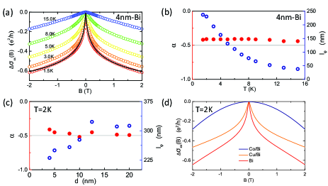
Next we focus on the weak anti-localization (WAL) peak. In Fig. 3(a) we show the magnetoresistance curves for several different temperatures. These curves are measured on a 4nm thick Bi film patterned into a Hall bar. The WAL peak is clearly observed. After detailed quantitative analysis we conclude that these magnetoresistance data are well described by the two dimensional Hikami-Larkin-Nagaoka (HLN) theory for transport in the presence of strong spin-orbit coupling
| (1) |
where , is the digamma function S. Hikami and Nagaoka. (1980). Treating (see later) and the phase coherence length as fitting parameters we fit the data to Eq. (1). An example of the quality of the fit is shown by the bottom data set (the black curve is the fit) of Fig. 3(a). In Fig. 3(b) we plot the fitted value (red dots) as a function of temperature, the result suggests is nearly temperature independent and is very close to -1/2. In contrast the fitted phase coherence length (blue dots) decreases monotonically with increasing temperature. In Fig. 3(c) we plot the fitted as a function of film thickness for a fixed temperature. Again is approximately thickness independent and stays very close to -1/2. Theoretically = -1/2 is expected for a connected spin-orbit interacting 2D system Nomura et al. (2007). The fact that our fitted value is close to -1/2 again attests for the fact that the metallic surface states of our Bi film (top, bottom, and side surfaces together) forms a continuous 2D spin-orbit metal as expected for the surface states of topological insulator.
In Fig. 3(d) we show the effects of scalar and magnetic impurity on WAL. From the line shape of the curves it is clear that the WAL peak remains as a 0.5 ML of non-magnetic Cu are introduced to the top surface. In contrast when we add a 0.25 ML of magnetic Co the WAL peak is completely gone. This result supports the notion that the surface states of our Bi film are protected by the time reversal symmetry just like the surface states of topological insulators.
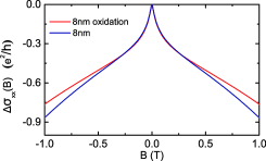
Before turning to theory, we checked that the metallic surface states of Bi(111) thin films are robust against surface oxidation. In growing an 8 nm thick Bi thin film we deliberately expose half of the sample to air (at 300 K) before capping. Interestingly such “violent act” only caused a merely 10 percent change in the total conductance. In Fig. 4 we show the effect of oxidization on the magnetoresistance curve in weak field. Clearly the WAL peak is robust against oxidization. These results are consistent with the picture that surface oxidation simply displaces the metallic surface toward the film interior.
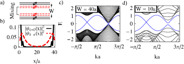
All the experimental data presented up to this point supports the idea that when Bi (which is topologically trivial in the bulk) is made into thin films they become topological insulators. Here we demonstrate, as a matter of principle, that a topologically trivial system can become topologically non-trivial as it becomes sufficiently thin. For simplicity we focus on a two dimensional system (the generalization to 3D is straightforward). The basic physics is illustrated in Fig. 5(a) where each edge possesses two pairs of counter propagating helical modes (black and red) when is wide. With impurities backscattering between the red and black modes is allowed, hence the system is topologically trivial. However if the red edge modes decay into the bulk with a much larger length scale than the black ones there will be an intermediate range in where backscattering between the red edge modes from opposite edges is sufficiently strong but that between the black ones is still extremely weak. For that range of the red modes will be gapped out and the system becomes indistinguishable from a strong topological insulator. The above physics can be demonstrated by an explicit model
| (2) |
Here are the Pauli matrices, , and . For , this model describes a trivial insulator, featuring two gapped Dirac cones at and with masses . For large (e.g., =40), this model has two pairs of counter-propagating edge modes centered at edge momenta and , see Fig. 5(c). Due to the difference in the masses the decay length of these two edge modes satisfy as Fig. 5(b) shows. Reducing makes states from opposite edges hybridize. However if , only the edge states hybridize significantly, causing them to open a gap (Fig. 5(d)). After that only one pair of edge states remain gapless and the system is indistinguishable from a strong topological insulator.
It is well known that bulk Bi is topologically trivial but Sb is topologically non-trivial. The difference between the bulk band structure of these two materials lies in the fact that gap inversion occurs at three time reversal invariant momenta, the L points, for Bi but not Sb. It is also known that the spin orbit induced gap at L points in Bi is very small ( meV) Brown et al. (1963) while the gap is large ( eV) at point Wang and Jain (1970); Hunderi (1975). They play the roles of the small and large Dirac masses respectively in the simple model above. To further check the existence of topological thin film state discussed above we have performed first-principle calculations for a superlattice made up of Bi slabs of varying thickness stacked in the (111) direction (we also can tune the coupling between adjacent slabs by adjusting the vacuum thickness between slabs). The result show that for both 12 BL and 15 BL Bi(111) slabs the artificial 3D system is topologically non-trivial because the gap at the L points becomes de-inverted. The detailed results will be presented elsewhere Wu and Feng .
In summary we have carried out extensive quantum transport measurements and performed simple model as well as first-principle calculations for Bi thin films. All of our results suggest that when made thin enough Bi becomes topologically non-trivial. We explain this result in terms of a simple physical picture. We stress that what we discuss here is entirely different from the predicted two dimensional topological insulator when Bi film is only one bilayer thick. Our result should point out a new direction in the search of topologically interesting materials.
Acknowledgements.
The authors thank S. Blügel, G. Bihlmayer and I. Aguilera for their valuable discussions. XFJ is supported by MOST (No. 2011CB921802) and NSFC (No. 11374057). DQ is supported by NSFC ( No. 11274228). JF is supported by NBRPC(2013CB921900). DHL and FdJ are supported by DOE Office of Basic Energy Sciences, Division of Materials Science, Material theory Program, grant DE-AC02-05CH11231..1
.1.1
References
- de Haase and van Alphen (1930) W. J. de Haase and P. M. van Alphen, Proc. Acad. Sci. 33, 1106 (1930).
- Ogrin et al. (1966) Y. F. Ogrin, V. N. Lutskii, and M. I. Elinson, JETP Lett. 7, 71 (1966).
- Abrikosov. (2000) A. A. Abrikosov., Europhys. Lett. 49, 789 (2000).
- Buckel and Hilsch (1954) W. Buckel and R. Hilsch, Z. Phys. 138, 109 (1954).
- Behnia et al. (2007) K. Behnia, L. Balicas, and Y. Kopelevich, Science 317, 1729 (2007).
- Hofmann (2006) P. Hofmann, Progress in Surface Science 81, 191 (2006).
- Xiao et al. (2012) S. Xiao, D. Wei, and X. Jin, Phys. Rev. Lett. 109, 166805 (2012).
- Hasan and Kane (2010) M. Z. Hasan and C. L. Kane, Rev. Mod. Phys. 82, 3045 (2010).
- Qi and Zhang (2011) X.-L. Qi and S.-C. Zhang, Rev. Mod. Phys. 83, 1057 (2011).
- Nagao et al. (2004) T. Nagao, J. T. Sadowski, M. Saito, S. Yaginuma, Y. Fujikawa, T. Kogure, T. Ohno, Y. Hasegawa, S. Hasegawa, and T. Sakurai, Phys. Rev. Lett. 93, 105501 (2004).
- Tian et al. (2005) C. S. Tian, D. Qian, D. Wu, R. H. He, Y. Z. Wu, W. X. Tang, L. F. Yin, Y. S. Shi, G. S. Dong, X. F. Jin, X. M. Jiang, F. Q. Liu, H. J. Qian, K. Sun, L. M. Wang, G. Rossi, Z. Q. Qiu, and J. Shi, Phys. Rev. Lett. 94, 137210 (2005).
- Yin et al. (2006) L. F. Yin, D. H. Wei, N. Lei, L. H. Zhou, C. S. Tian, G. S. Dong, X. F. Jin, L. P. Guo, Q. J. Jia, and R. Q. Wu, Phys. Rev. Lett. 97, 067203 (2006).
- Tian et al. (2009) Y. Tian, L. Ye, and X. Jin, Phys. Rev. Lett. 103, 087206 (2009).
- Matsuda et al. (2007) I. Matsuda, C. Liu, T. Hirahara, M. Ueno, T. Tanikawa, T. Kanagawa, R. Hobara, S. Yamazaki, S. Hasegawa, and K. Kobayashi, Phys. Rev. Lett. 99, 146805 (2007).
- (15) M. Yao and D. Qian, to be published .
- Al’tshuler B. L. (1981) S. B. Z. Al’tshuler B. L., Aronov A. G., JETP Lett. 33, 94 (1981).
- Lee et al. (1987) P. A. Lee, A. D. Stone, and H. Fukuyama, Phys. Rev. B 35, 1039 (1987).
- S. Hikami and Nagaoka. (1980) A. L. S. Hikami and Y. Nagaoka., Prog. Theor. Phys. 63, 707 (1980).
- Nomura et al. (2007) K. Nomura, M. Koshino, and S. Ryu, Phys. Rev. Lett. 99, 146806 (2007).
- Brown et al. (1963) R. N. Brown, J. G. Mavroides, and B. Lax, Phys. Rev. 129, 2055 (1963).
- Wang and Jain (1970) P. Y. Wang and A. L. Jain, Phys. Rev. B 2, 2978 (1970).
- Hunderi (1975) O. Hunderi, J. Phys. F. 5, 2214 (1975).
- (23) M. Wu and J. Feng, to be published .