Experimental determination of Rashba spin-orbit coupling in wurtzite -GaN:Si
Abstract
Millikelvin magnetotransport studies are carried out on heavily -doped wurtzite GaN:Si films grown on semi-insulating GaN:Mn buffer layers by metal-organic vapor phase epitaxy. The dependence of the conductivity on magnetic field and temperature is interpreted in terms of theories that take into account disorder-induced quantum interference of one-electron and many-electron self-crossing trajectories. The Rashba parameter meVÅ is determined, and it is shown that in the previous studies of electrons adjacent to GaN/(Al,Ga)N interfaces, bulk inversion asymmetry was dominant over structural inversion asymmetry. The comparison of experimental and theoretical values of across a series of wurtzite semiconductors is presented as a test of current relativistic ab initio computation schemes. Low temperature decoherence is discussed in terms of disorder-modified electron-electron scattering.
pacs:
71.70.Ej, 72.15.Rn, 72.80.Ey, 72.20.-iI Introduction
Beside being strategic materials systems for nowadays optoelectronicMorkoç (2009) and high-power applications,Morkoç (2009); Palacios et al. (2005) GaN and related alloys are expected to play a major role in the realization of spin-related functionalities based on semiconductors. In particular, Fe doping serves routinely to fabricate semi-insulating GaN substrates.Kaun et al. (2013) However, GaN with higher Fe concentrations exhibits room temperature ferromagneticBonanni et al. (2008); Navarro-Quezada et al. (2010) and antiferromagneticNavarro-Quezada et al. (2010) features associated with the aggregation of Fe cations, leading to the formation of various magnetically robust FexN nanocrystals. Furthermore, light absorption associated with the Mn mid-gap band in GaN improves the efficiency of GaN-based solar cells.Sheu et al. (2013) At the same time, the formation of Mn-Mgk impurity complexes activates room temperature infrared luminescence,Devillers et al. (2012) suggesting that the optoelectronic capabilities of nitrides can be extended towards the communication windows.
Other appealing aspects of these systems are associated with spin-orbit coupling (SOC). On the one hand, the small value of the nitrogen proton number , leading to weak spin-orbit splitting of the valence band, results in a long spin relaxation time of electrons in GaN.Beschoten et al. (2001); Krishnamurthy et al. (2003) On the other hand, strong interfacial electric fields result in substantial Rashba-type SOC that in the extreme case of GaN/InN/GaN quantum wells may lead to a transition to the topological insulator phase.Miao et al. (2012) In this context particularly appealing is the demonstration that (Ga,Mn)N is a dilute ferromagnetic insulator,Bonanni et al. (2011); Sawicki et al. (2012); Stefanowicz et al. (2013) which offers prospects to the search for phenomena associated with the interplay between SOC and the exchange splitting of bands by ferromagnetic proximity effects.Sau et al. (2010)
Here, we report on experimental studies of weak localization and antilocalization magnetoresistance in epitaxial layers of wurtzite (wz) -GaN:Si. A theoretical description of the data in terms of the Hikami, Larkin, and Nagaoka theory,Hikami et al. (1980) suitably adapted for wz compounds,Sawicki et al. (1986) allows us to extract the magnitude of the parameter describing the Rashba term linear in and accounting for the spin-splitting of the conduction band in bulk wz semiconductors.Rashba (1960) This term is specific to the crystal structure in question and its presence is not associated with interfacial electric fields.Bychkov and Rashba (1984) The value of ) meVÅ we determine here is by two orders of magnitude greater than the one found by electron spin resonance (ESR) for electrons trapped by donors or accumulated at the surface of -GaN.Wolos et al. (2011) At the same time, it agrees with the value found for electrons attracted to the GaN/(Al,Ga)N interface by polarization electric fields.Schmult et al. (2006); Kurdak et al. (2006); Thillosen et al. (2006a, b); Zhou et al. (2008); Cheng et al. (2008); Belyaev et al. (2008) Our results demonstrate, therefore, that the bulk rather than the structure inversion asymmetry accounts for the spin splitting of interfacial states. We discuss also the chemical trends in and show that the discrepancy between the current ab initio theoriesLew Yan Voon et al. (1996); Majewski and Vogl (2005) and the present and previous magnetoresistance,Sawicki et al. (1986); Andrearczyk et al. (2005) opticalRomestain et al. (1977); Dobrowolska et al. (1984) and ESR studiesKozuka et al. (2013) is within a factor of two for various wz--type semiconductors: ZnO, GaN, CdS, and CdSe. Finally, we treat the temperature dependence of the phase coherence length and conductivity in terms of electron-electron interactions in disordered systems.Altshuler and Aronov (1985); Lee and Ramakrishnan (1985); Altshuler et al. (1982a)
II samples and experiment
The Si-doped GaN layers considered in the present study have been grown in an AIXTRON 200RF horizontal tube metalorganic vapor phase epitaxy (MOVPE) reactor and deposited on a -plane sapphire substrate using TMGa, MnCp2, NH3, and SiH4 as precursors for Ga, Mn, N, and Si respectively, with H2 as carrier gas. After nitridation of the sapphire substrate, a low temperature nucleation layer (NL) is deposited at 540∘C and then annealed at 1040∘C. Successively, a 1 m-thick GaN:Mn buffer layer is grown also at 1040∘C, Mn being introduced in order to compensate the -type background proper of the GaN layers fabricated by MOVPE. The concentration of Mn in the buffer layer is as low as 0.06%, as confirmed by secondary-ion mass spectroscopy (SIMS) and SQUID magnetometry. A 150 nm layer of GaN:Si is further grown at 1000∘C onto the GaN:Mn buffer layer. All steps of the growth process are monitored with in situ spectroscopic and kinetic ellipsometry.
The grown samples are systematically characterized by atomic force microscope (AFM), high resolution x-ray diffraction (HRXRD), high resolution transmission electron microscopy (HRTEM) and SIMS has been employed for chemical analysis. The AFM micrographs reveal a flat surface (rms roughness 1 nm) while HRXRD and HRTEM confirm the high crystallinity of the samples. The HRTEM analysis does not reveal any secondary phases like precipitates of SixN, and energy dispersive x-ray spectroscopy (EDS) states the homogeneous distribution of Si in the doped layer with a concentration of 0.24%, in agreement with SIMS data.
The magnetotransport measurements have been performed on Hall bars with Ti/Au/Al/Ti/Au metallic contacts fabricated by conventional photolithography. Transport experiments down to 40 mK have been carried out in a dedicated home-built helium cryostat and a dilution refrigerator. The electron concentration obtained from the Hall data is found to be constant over a wide range of temperatures and to have a value cm-3, far over the critical value for the metal-to-insulator (MIT) transition in bulk GaN, cm-3.Ferreira da Silva and Persson (2002) The degenerate and metallic character of the samples is further documented by the absence of dependence of on the temperature in the limit , as well as by the values of the Hall mobility cm2/Vs and in this regime, where is the mean free path. Accordingly, we interpret the measured magnetoresistance in terms of quantum corrections to the conductivity of disordered systems, developed for and .Altshuler and Aronov (1985); Lee and Ramakrishnan (1985)
III experimental results
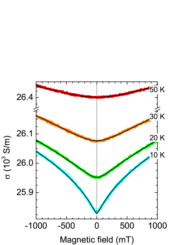
In Figs. 1 and 2 the conductivity of the GaN:Si film is shown at different temperatures as a function of the magnetic field applied perpendicular to the film surface, parallel to the wz--axis. It is seen from Fig. 1 that for K the magnetoconductivity (MC) is solely positive, while from the data collected in Fig. 2 for K and down to 40 mK there are contributions of both negative and positive MC in low magnetic fields. This negative component of MC is related to the appearance of a weak antilocalization (WAL) maximum (which vanishes above 1 K), a distinct signature of SOC.
For K, the experimental results are fitted within a three dimensional (3D) theoretical model of weak localization MC in semiconductors on the metallic side of the MIT, as proposed by Kawabata.Kawabata (1980a) Here, the phase coherence length is the only fitting parameter. As seen, the theory describes the data quite accurately. We add that the presence of positive MC is often taken as an indication for spin disorder scattering. Actually, even in the presence of magnetic impurities, spin disorder scattering is typically masked by other scattering mechanisms in semiconductors, and rarely perturbs the conductivity directly.
However, this 3D model does not describe the observed MC for K and low magnetic fields, where two additional aspects must be considered, namely: (i) the impact of SOC on the quantum corrections to the conductivity, leading to a WAL maximum in MC below 1 K (as seen in Fig. 2) and (ii) a dimensional crossover from 3D to 2D that occurs if , where is the layer thickness. In Fig. 2, the fingerprint of WAL is observed for K and for mT. The MC data obtained for K are fitted with the theoretical model proposed for 2D films in the weakly localized regime, , and considering effects of spin-dependent scattering.Hikami et al. (1980)
According to the theory, SOC in wz semiconductors leads to a term linear in in the effective mass equation,Rashba (1960); Casella (1960)
| (1) |
where is the Rashba parameter; is the versor along the wz--axis, and are the Pauli matrices. For , the corresponding spin relaxation times are given by,Altshuler et al. (1982b)
| (2) |
where the axis is taken along the wz--axis, is the momentum relaxation time, and he effective mass is for GaN.Witowski et al. (1999)
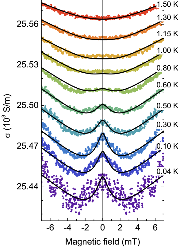
Here, two fitting parameters and , are employed to describe the conductivity changes in magnetic field. From the fitting of the MC data in the low temperature range, we find for wz--GaN:Si to be meVÅ. Within the experimental uncertainties, this value is virtually identical to the one determined by the interfacial polarization electric field in numerous MC studies of a 2D electron gas adjacent to the GaN/(Al,Ga)N interface.Schmult et al. (2006); Kurdak et al. (2006); Thillosen et al. (2006a, b); Zhou et al. (2008); Cheng et al. (2008) This agreement means that the Rashba spin relaxation associated with the wz crystal structure dominates over effects brought about by the interfacial field . This also explains why the value of determined for GaN/(Al,Ga)N heterostructures was found to be independent of the gate electric field and of the Al content in the barrier.Thillosen et al. (2006b)
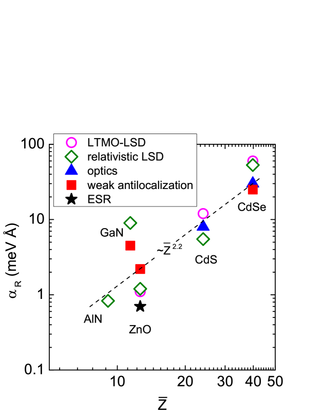
In Fig. 3 we provide a compilation of values determined through various experimental methods for wz semiconductor compounds, plotted as a function of a harmonic average of the cation and anion proton numbers, , and compared to results of ab initio computations in the framework of the density functional theory with relativistic effects taken into account non-perturbatively.Majewski et al. (2004) A chemical trend, , is evident and confirms that the significance of the SOC increases with the square of the nucleus charge. Furthermore, it is seen that the theory describes the experimental values with an accuracy better than a factor of two.
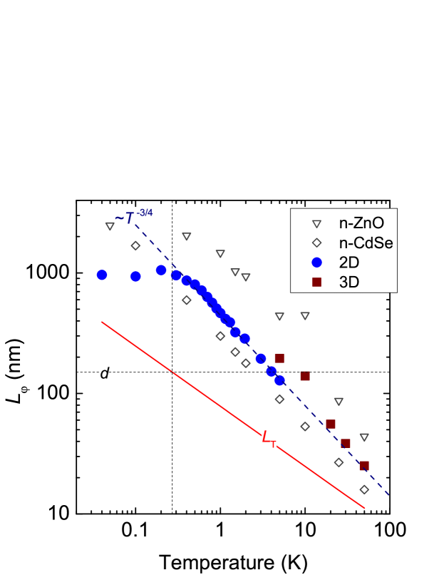
Our fitting procedure provides also the values of , which are shown in Fig. 4, and compared to corresponding data for CdSe:In (Ref. Sawicki et al., 1986) and ZnO:Al (Ref. Andrearczyk et al., 2005). A dependence is observed for all compounds over a wide temperature range, a behavior expected theoretically for decoherence brought about by electron-electron interactions in disordered 3D systems.Altshuler et al. (1982a); Altshuler and Aronov (1985) A transition to the 2D case occurs in this case at . A change in the slope observed in this region, if not caused by noise-related decoherence, can be associated with the dimensional cross-over.
According to theoretical expectations, has the same functional form for electron-electron scattering with large and small energy transfers in the 3D case.Altshuler et al. (1982a) The relaxation times corresponding to these two contributions are given by,Altshuler et al. (1982a); Altshuler and Aronov (1985)
| (3) |
where the energy of quasiparticles is identified with , is the density of states at the Fermi level, and is the coupling parameter in the triplet channel. This parameter controls also the temperature dependence of the conductivity at low temperatures, whose studies lead to for CdSe:In (Ref. Sawicki et al., 1986) and for GaN:Si, as discussed below.
By taking and , we evaluate and 1670 nm K3/4 for the sample of CdSe:In and GaN:Si, respectively, where is the prefactor in the dependence . Furthermore, our estimation confirms that scattering with large energy transfers dominates, . However, the theoretical values of are for both materials greater than those implied by the experimental data presented in Fig. 4, for which and 440 nm K3/4, respectively.
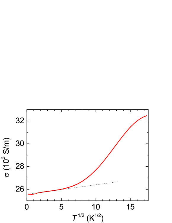
In Fig. 5 the zero magnetic field conductivity is reported as a function of , and it is seen to have a linear dependence on square root of temperature below 25 K. This behavior is assigned to quantum corrections to the conductivity due to disorder-modified electron-electron interactions.Altshuler and Aronov (1985); Lee and Ramakrishnan (1985) A quantitative comparison of this slope to the theory leads to a value of the coupling parameter in the triplet channel . This relatively small value can be expected for . However, on approaching the metal-to-insulator transition the value of increases. This effect was observed in -CdSe, where and the conductivity decreases with increasing temperature.Sawicki et al. (1986)
IV conclusions
In summary, we have carried out low temperature magnetotransport studies on high quality heavily doped wz-GaN:Si films grown on a semi-insulating GaN:Mn buffer layer. Our investigations reconfirm the relevance, in doped degenerate semiconductors, of disorder-induced quantum interference of one-electron and many-electron self-crossing trajectories, effects not captured by the Drude-Boltzmann description of transport phenomena. The quantitative models of the magnetoconductance data have allowed us to determine the Rashba parameter , so far known only from studies of 2DEG adjacent to GaN/(Al,Ga)N interfaces. Our results demonstrate that inversion asymmetry associated with the wurtzite crystal structure dominates over the effects of the interfacial electric field in the conduction band of GaN. The comparison of experimental and theoretical values of across a series of wz semiconductors has provided an important test of the current relativistic ab initio computation schemes, demonstrating that the differences between the experimental and theoretical values are within a factor of two. Furthermore, our quantitative interpretation of the decoherence length has confirmed that electron-electron scattering is a dominant source of phase breaking in these systems. With these premises, wide perspectives open for nitrides, as building-blocks for the next generation of spin devices exploiting spin-orbit coupling and the magnetism of transition-metal doped layers.
acknowledgments
This work was supported by the FunDMS Advanced Grant of the European Research Council (ERC Grant No. 227690) within the Ideas 7th Framework Programme of the European Union, and by the Austrian Science Foundation – FWF (P20065, P22477, and P24471), and by National Science Centre (Poland) under OPUS grants No. 2011/03/B/ST3/02457 and 2013/09/B/ST3/04175.
References
- Morkoç (2009) H. Morkoç, Handbook of Nitride Semiconductors and Devices: GaN-based Optical and Electronic Devices, Vol. 3 (Wiley-VCH, Weinheim, 2009).
- Palacios et al. (2005) T. Palacios, A. Chakraborty, S. Rajan, C. Poblenz, S. Keller, S. DenBaars, J. Speck, and U. Mishra, IEEE Electron Device Lett. 26, 781 (2005).
- Kaun et al. (2013) S. W. Kaun, M. H. Wong, U. K. Mishra, and J. S. Speck, Semicond. Sci. Technol. 28, 074001 (2013).
- Bonanni et al. (2008) A. Bonanni, A. Navarro-Quezada, T. Li, M. Wegscheider, Z. Matěj, V. Holý, R. T. Lechner, G. Bauer, M. Rovezzi, F. D’Acapito, M. Kiecana, M. Sawicki, and T. Dietl, Phys. Rev. Lett. 101, 135502 (2008).
- Navarro-Quezada et al. (2010) A. Navarro-Quezada, W. Stefanowicz, T. Li, B. Faina, M. Rovezzi, R. T. Lechner, T. Devillers, F. d’Acapito, G. Bauer, M. Sawicki, T. Dietl, and A. Bonanni, Phys. Rev. B 81, 205206 (2010).
- Sheu et al. (2013) J.-K. Sheu, F.-W. Huang, C.-H. Lee, M.-L. Lee, Y.-H. Yeh, P.-C. Chen, and W.-C. Lai, Appl. Phys. Lett. 103, 063906 (2013).
- Devillers et al. (2012) T. Devillers, M. Rovezzi, N. G. Szwacki, S. Dobkowska, W. Stefanowicz, D. Sztenkiel, A. Grois, J. Suffczyński, A. Navarro-Quezada, T. Faina, B. Li, P. Glatzel, F. d’Acapito, R. Jakieła, M. Sawicki, J. A. Majewski, T. Dietl, and A. Bonanni, Sci. Rep. 2 (2012).
- Beschoten et al. (2001) B. Beschoten, E. Johnston-Halperin, D. K. Young, M. Poggio, J. E. Grimaldi, S. Keller, S. P. DenBaars, U. K. Mishra, E. L. Hu, and D. D. Awschalom, Phys. Rev. B 63, 121202 (2001).
- Krishnamurthy et al. (2003) S. Krishnamurthy, M. van Schilfgaarde, and N. Newman, Appl. Phys. Lett. 83, 1761 (2003).
- Miao et al. (2012) M. S. Miao, Q. Yan, C. G. Van de Walle, W. K. Lou, L. L. Li, and K. Chang, Phys. Rev. Lett. 109, 186803 (2012).
- Bonanni et al. (2011) A. Bonanni, M. Sawicki, T. Devillers, W. Stefanowicz, B. Faina, T. Li, T. E. Winkler, D. Sztenkiel, A. Navarro-Quezada, M. Rovezzi, R. Jakieła, A. Grois, M. Wegscheider, W. Jantsch, J. Suffczyński, F. D’Acapito, A. Meingast, G. Kothleitner, and T. Dietl, Phys. Rev. B 84, 035206 (2011).
- Sawicki et al. (2012) M. Sawicki, T. Devillers, S. Gałȩski, C. Simserides, S. Dobkowska, B. Faina, A. Grois, A. Navarro-Quezada, K. N. Trohidou, J. A. Majewski, T. Dietl, and A. Bonanni, Phys. Rev. B 85, 205204 (2012).
- Stefanowicz et al. (2013) S. Stefanowicz, G. Kunert, C. Simserides, J. A. Majewski, W. Stefanowicz, C. Kruse, S. Figge, T. Li, R. Jakieła, K. N. Trohidou, A. Bonanni, D. Hommel, M. Sawicki, and T. Dietl, Phys. Rev. B 88, 081201 (2013).
- Sau et al. (2010) J. D. Sau, R. M. Lutchyn, S. Tewari, and S. Das Sarma, Phys. Rev. Lett. 104, 040502 (2010).
- Hikami et al. (1980) S. Hikami, A. I. Larkin, and Y. Nagaoka, Prog. Theo. Phys. 63, 707 (1980).
- Sawicki et al. (1986) M. Sawicki, T. Dietl, J. Kossut, J. Igalson, T. Wojtowicz, and W. Plesiewicz, Phys. Rev. Lett. 56, 508 (1986).
- Rashba (1960) E. I. Rashba, Sov. Phys. Solid State 2, 1109 (1960).
- Bychkov and Rashba (1984) Y. A. Bychkov and E. I. Rashba, J. Phys. C 17, 6039 (1984).
- Wolos et al. (2011) A. Wolos, Z. Wilamowski, C. Skierbiszewski, A. Drabinska, B. Lucznik, I. Grzegory, and S. Porowski, Physica B 406, 2548 (2011).
- Schmult et al. (2006) S. Schmult, M. J. Manfra, A. Punnoose, A. M. Sergent, K. W. Baldwin, and R. J. Molnar, Phys. Rev. B 74, 033302 (2006).
- Kurdak et al. (2006) C. Kurdak, N. Biyikli, U. Özgür, H. Morkoç, and V. I. Litvinov, Phys. Rev. B 74, 113308 (2006).
- Thillosen et al. (2006a) N. Thillosen, T. Schäpers, N. Kaluza, H. Hardtdegen, and V. A. Guzenko, Appl. Phys. Lett. 88, 022111 (2006a).
- Thillosen et al. (2006b) N. Thillosen, S. Cabañas, N. Kaluza, V. A. Guzenko, H. Hardtdegen, and T. Schäpers, Phys. Rev. B 73, 241311 (2006b).
- Zhou et al. (2008) W. Z. Zhou, T. Lin, L. Y. Shang, L. Sun, K. H. Gao, Y. M. Zhou, G. Yu, N. Tang, K. Han, B. Shen, S. L. Guo, Y. S. Gui, and J. H. Chu, J. Appl. Phys. 104, 053703 (2008).
- Cheng et al. (2008) H. Cheng, N. Biyikli, Özgür, Ç. Kurdak, H. Morkoç, and V. I. Litvinov, Physica E 40, 1586 (2008).
- Belyaev et al. (2008) A. E. Belyaev, V. G. Raicheva, A. M. Kurakin, N. Klein, and S. A. Vitusevich, Phys. Rev. B 77, 035311 (2008).
- Lew Yan Voon et al. (1996) L. C. Lew Yan Voon, M. Willatzen, M. Cardona, and N. E. Christensen, Phys. Rev. B 53, 10703 (1996).
- Majewski and Vogl (2005) J. A. Majewski and P. Vogl, AIP Conf. Proc. 772, 1403 (2005).
- Andrearczyk et al. (2005) T. Andrearczyk, J. Jaroszyński, G. Grabecki, T. Dietl, T. Fukumura, and M. Kawasaki, Phys. Rev. B 72, 121309 (2005).
- Romestain et al. (1977) R. Romestain, S. Geschwind, and G. E. Devlin, Phys. Rev. Lett. 39, 1583 (1977).
- Dobrowolska et al. (1984) M. Dobrowolska, A. Witowski, J. K. Furdyna, T. Ichiguchi, H. D. Drew, and P. A. Wolff, Phys. Rev. B 29, 6652 (1984).
- Kozuka et al. (2013) Y. Kozuka, S. Teraoka, J. Falson, A. Oiwa, A. Tsukazaki, S. Tarucha, and M. Kawasaki, Phys. Rev. B 87, 205411 (2013).
- Altshuler and Aronov (1985) B. Altshuler and A. Aronov, in Electron-Electron Interactions in Disordered Systems, Modern Problems in Condensed Matter Sciences, Vol. 10, edited by A. Efros and M. Pollak (Elsevier, Amsterdam, 1985) pp. 1 – 153.
- Lee and Ramakrishnan (1985) P. A. Lee and T. V. Ramakrishnan, Rev. Mod. Phys. 57, 287 (1985).
- Altshuler et al. (1982a) B. L. Altshuler, A. G. Aronov, and D. E. Khmelnitsky, J. Phys. C 15, 7367 (1982a).
- Ferreira da Silva and Persson (2002) A. Ferreira da Silva and C. Persson, J. Appl. Phys 92, 2550 (2002).
- Kawabata (1980a) A. Kawabata, J. Phys. Soc. Jpn. 49, 628 (1980a).
- Kawabata (1980b) A. Kawabata, Solid State Commun. 34, 431 (1980b).
- Casella (1960) R. C. Casella, Phys. Rev. Lett. 5, 371 (1960).
- Altshuler et al. (1982b) B. L. Altshuler, A. G. Aronov, D. E. Khmelnitskii, and A. I. Larkin, in Quantum Theory of Solids, edited by I. M. Lifshits (Mir, Moscow, 1982) p. 130.
- Witowski et al. (1999) A. M. Witowski, K. Pakuła, J. M. Baranowski, M. L. Sadowski, and P. Wyder, Appl. Phys. Lett. 75, 4154 (1999).
- Majewski et al. (2004) J. A. Majewski, S. Birner, A. Trellakis, M. Sabathil, and P. Vogl, Phys. Stat. Sol. (c) 1, 2003 (2004).