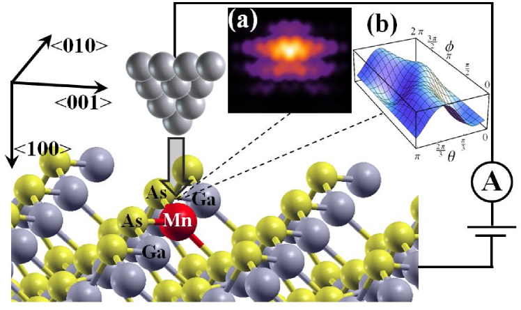
Trend of the magnetic anisotropy for individual Mn dopants near the (110) GaAs surface
Abstract
Using a microscopic finite-cluster tight-binding model, we investigate the trend of the magnetic anisotropy energy as a function of the cluster size for an individual Mn impurity positioned in the vicinity of the (110) GaAs surface, We present results of calculations for large cluster sizes, containing approximately atoms, which have not been investigated so far. Our calculations demonstrate that the anisotropy energy of a Mn dopant in bulk GaAs found to be non-zero in previous tight-binding calculations, is purely a finite size effect and it vanishes as the inverse cluster size. In contrast to this, we find that the splitting of the three in-gap Mn acceptor energy levels converges to a finite value in the limit of infinite cluster size. For a Mn in bulk GaAs this feature is related to the nature of the mean-field treatment of the coupling between the impurity and its nearest neighbors atoms. Moreover, we calculate the trend of the anisotropy energy in the sublayers, as the Mn dopant is moved away from the surface towards the center of the cluster. Here the use of large cluster sizes allows us to position the impurity in deeper sublayers below the surface, compared to previous calculations. In particular, we show that the anisotropy energy increases up to the fifth sublayer and then decreases as the impurity is moved further away from the surface, approaching its bulk value. The present study provides important insight for experimental control and manipulation of the electronic and magnetic properties of individual Mn dopants at the semiconductor surface by means of advanced scanning tunneling microscopy techniques.
pacs:
75.50.Pp, 71.55.Eq1 Introduction
The past decade has witnessed a surge of interest in understanding and actively controlling
electronic, optical and magnetic properties of solitary dopants in semiconductors.
A corresponding sub-division of semiconductor electronics, known as solotronics (solitary dopant optoelectronics),
has emerged in recent years, with the focus on building novel devices that would make use of specific properties of
individual dopants, as well as on advancing our fundamental understanding of these atomic-scale systems [1].
The experimental progress in this field has been largely driven by
remarkable advances in using scanning tunneling microscopy (STM) to custom engineer, manipulate and characterize
single impurities on surfaces with atomic precision [2, 3].
In a number of key experiments, STM based techniques were used to study the electronic structure and
the magnetic interactions of
substitutional transition-metal (TM) dopants at semiconductor surfaces
[4, 5, 3, 6, 7, 8, 9, 10, 11].
On the theoretical side, both first-principles calculations [12, 13, 14, 15, 16, 17]
and microscopic tight-binding (TB)
models [18, 19, 20, 21, 22, 23, 24, 25, 26] have
played an essential role in elucidating experimental findings and predicting new properties.
Computationally efficient and physically motivated
TB models have been particularly successful in describing electronic and magnetic properties of some TM
impurities, such as Mn dopants with their associated acceptor states [18, 19, 21, 22, 23, 24, 26]
and, more recently, Fe dopants [27] on the (110) GaAs surface.
Due to their computational feasibility, microscopic TB models are especially well suited to study
single impurities as they allow the use of large supercells, with sizes exceeding
those accessible by first-principles approaches by several orders of magnitude.
Such models allow the calculation of measurable physical quantities, which can be
directly probed
in experiments (see Figure 1). In particular, finite-cluster TB calculations
provide a detailed description of the in-gap electronic structure in the presence of the dopant close to the
surface, which can be directly
related to resonances in conductance spectra measured by STM [22, 27].
Although a more elaborate treatment is required for
simulations of STM topographic images, in the first approximation the tunneling current is
proportional to the local density of states (LDOS) at the surface [28]. Therefore,
typically there is a strong correlation between the calculated LDOS
maps for dopants positioned on the surface or in subsurface layers and the
corresponding STM topographies [18, 19, 21, 22, 23, 24, 26]. Moreover, calculations
of magnetic anisotropy energy of TM dopants, which are accessible with current TB approaches,
provide an important input for interpreting and predicting the results of on-going experiments, aimed
at manipulating the magnetic moment of the dopant, e.g. by means of an external magnetic field.
Recently, TB calculations of the magnetic anisotropy landscape, combined with analysis of the shape and
the spatial extent of the acceptor
wavefunction, have been used to explain experimental results on magnetic-field
manipulation of a single Mn acceptor near the (110) GaAs surface [26].
A similar strategy has been used to predict the effect of the magnetic field on the magnetic moment of Fe in GaAs
and its dependence on the valence state of the dopant [27].
Here we report on recent advances in TB modeling of single substitutional Mn impurities, positioned near the (110) GaAs surface. We use a fully microscopic tight-binding model, hereafter referred to as a quantum-spin model, which includes explicitly -, - and -orbitals of the impurity atom [27]. This is in contrast to the classical-spin model used in earlier work [18, 22], where the Mn impurity spin is introduced as an effective classical vector, exchange-coupled to the quantum spins of the nearest-neighbor As atoms. We find an overall agreement with the results of previous work, in particular with the classical-spin model of reference [22]. Among the key features that have been already reported in [22] and that are well reproduced with our present model, are (i) the strongly localized and anisotropic character of the mid-gap Mn acceptor state and (ii) the dependence of the acceptor binding energy and magnetic anisotropy energy on the Mn position with respect to the surface. These features have been also observed experimentally in [3, 8] and in [9], respectively.
In the present paper we clarify and resolve some outstanding theoretical and computational issues, which have not been addressed in previous work. Importantly, we present calculations of the in-gap level structure and magnetic anisotropy energy for both Mn in the bulk and on the surface for increasing cluster size. We show that the fictitious anisotropy energy for Mn in the bulk, found previously [22], is a finite-size effect caused by the limited size of the supercell used in earlier calculations. Here we calculate explicitly the anisotropy energy for Mn in bulk GaAs using large clusters counting up to atom. We find that the anisotropy energy tends to zero with increasing the cluster size. Also, by employing lager clusters for surface calculations we show that the surface anisotropy energy indeed mimics its bulk counterpart when Mn is positioned deep below the surface.
Another feature that persisted in earlier calculations for Mn in the bulk is the emergence of
three non-degenerate levels in
GaAs gap (one of the levels is unoccupied and is therefore interpreted as an acceptor).
It is known that the three levels appearing in the gap should be degenerate in the perfectly
tetragonal environment of an impurity in bulk GaAs, even in the presence of the spin-orbit coupling [29].
Here we show that the lifting of the
degeneracy in actual TB calculations is not a finite-size effect. Instead, it is related to the breaking
of the rotational symmetry in mean-field-like treatments of the kinetic-exchange coupling between
the TM impurity -levels and the -levels of the nearest neighbor As atoms.
Finally, we present a comprehensive study of the magnetic anisotropy energy
of a single Mn acceptor as a function of its position in the subsurface layers. The finite-size
effects, stemming from the limited size of the supercell in this type of
calculations, have been identified and, to a great extent, controlled
by systematically increasing the cluster size. Such detailed knowledge of the
magnetic anisotropy energy, together with the calculated LDOS of the impurity-induced states in the gap,
are crucial for a quantitative comparison with STM experiments, especially in the presence of
external electric and magnetic fields [26, 27].
The rest of the paper is organized as follows. In the next section we describe the details of our microscopic TB approach and discuss some
computational issues related to the use of large supercells.
Section 3 contains the results of the calculations, namely
the electronic energy spectrum and the magnetic anisotropy of
the Mn acceptor on the (110) GaAs surface and subsurfaces for different
cluster size. We also provide a
quantitative comparison with the results of the classical-spin model,
reported previously [22],
as well as with calculations carried out using the present model for smaller
clusters [27].
Finally, we draw some conclusions.
2 Microscopic tight-binding model
We consider a finite cluster of GaAs, where substitutional TM impurities are introduced at Ga sites. The system is described by a multi-orbital TB model, with parameters inferred from density functional theory (DFT) calculations [27]. We include -, - and -orbitals for the impurity atoms while keeping only - and -orbitals for the atoms of the host. This choice of the orbital basis is motivated by DFT calculations, which show that the -levels of Ga are located far below ( 15 eV) the Fermi level [27]. The Hamiltonian of the system is given by
| (1) |
The first term in Equation (1) represents the TB Hamiltonian of the GaAs host, which can be further written as the sum of two terms
| (2) |
where
| (3) |
is the Slater-Koster Hamiltonian for bulk GaAs [30, 31, 32], with parameters representing both on-site energies and nearest-neighbors hopping integrals. Here and are electron creation and annihilation operators; and are atomic indices that run over all atoms other than the impurity, and are orbital indices and is a spin index defined with respect to an arbitrary quantization axis. The spin-orbit interaction (SOI) is introduced as an on-site one-body term
| (4) |
where are the
re-normalized spin-orbit splittings [30].
The second term
in Equation (1) is the Hamiltonian of the TM impurity.
We have
where and are creation and annihilation operators
at the impurity site ; the orbital index runs over -, -, and -orbitals.
The first term in
Equation (2) describes the hopping between the impurity and its nearest-neighbors As atoms.
For the TB hopping parameters between the impurity -orbitals and the nearest-neighbor
As - and -orbitals we use the same values as for the corresponding hopping parameters
between Ga and As [33].
The second term in Equation (2) represents on-site energies of the impurity for a given orbital.
The -orbital energies play an important role in the model.
Their values for “spin-up” (majority)
and “spin-down” (minority) electrons
are different, which leads to a different occupation for opposite spin states,
and hence to a non-zero spin magnetic moment at the impurity site.
As a first estimate of the on-site -orbital energies, we use the values of the exchange-split
majority and minority -levels, which can be identified
in the spin- and orbital-resolved density of states (DOS) of the impurity, calculated with DFT.
For the exact parametrization of the TM impurity Hamiltonian the
reader is referred to reference [27], where the model was first introduced.
The last term in Equation (2) is an on-site SOI term for the impurity atom,
analogous to the one given in Equation (4). The SOI terms and
will cause the total ground-state energy of the system
to depend on the direction of the impurity magnetic moment,
defined with respect to an arbitrary quantization axis. This is the origin of the magnetic anisotropy energy.
Finally, the third term
in Equation (1)
| (5) |
is a long-range repulsive Coulomb
potential that is dielectrically screened by the host material
(the index runs over all impurity atoms), with being the dielectric
constant. This term prevents the charging of the impurity atom
and localizes the acceptor hole around the impurity [22].
The electronic structure of GaAs with a single substitutional Mn impurity atom
is obtained by performing supercell-type calculations
with periodic boundary conditions applied in either 2 or 3 dimensions, depending on
whether we are studying the surface or a bulk-like
system.
We do not take into account the
modification in strain and relaxation caused by the presence
of the magnetic impurity. However
in order to remove
artificial dangling-bond states that would otherwise appear in the
band gap, we include relaxation of surface layer positions,
following a procedure put forward in
Refs. [34] and [35].
For more details the reader is
referred to reference [22].
Based on our computational resources, we were able to
fully diagonalize and obtain the entire eigenvalue spectrum of
the Hamiltonian for clusters with up to 3200 atoms.
For the clusters larger than 3200 atoms,
we used the Lanczos method, built-in a commercial software
package, MATLAB [36], which allowed us to compute eigenvalues
in a narrow window of interest (typically few eigenvalues around the
expected position of the Mn acceptor in the gap). The
outputs of the two methods were systematically compared
to insure the stability
of the results against the variation of
the diagonalization procedure.
3 Results and discussion
We present the results of calculations carried out for a single Mn dopant in bulk GaAs and near the
(110) GaAs surface using the quantum-spin model, described in the previous section. The size of
the supercell in our TB model is varied between 3200 atoms, which is the maximum size that has
been investigated previously, to 30,000 atoms.
In general, our calculations produce the well-known features of Mn in the bulk as well as on the
surface, in agreement with previous theoretical work [22].
However, as we show in the following, the model gives a better and more realistic estimate of
the Mn magnetic anisotropy energy and its dependence on the impurity position below the surface, as
the size of the cluster is increased.
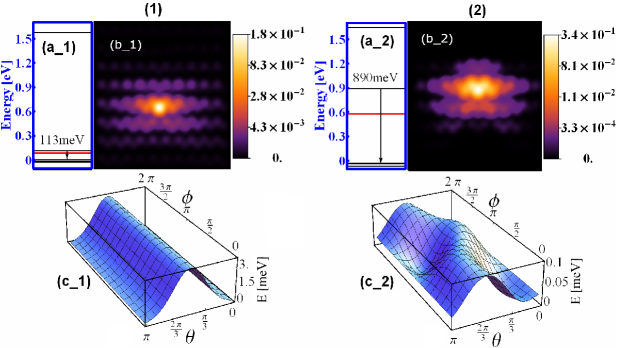
Figure 2 shows the in-gap electronic structure,
the acceptor LDOS and the anisotropy landscape for Mn in the bulk
(left panels) and on the (110) surface
(right panels) of GaAs.
Angles and used in panels (c_1) and (c_2) and throughout
the paper, are defined such way that is parallel
to the [001] and (, ) is parallel to [010] crystalline directions.
As it is shown in panels (a_1) and (a_2), Mn introduces three levels in the GaAs gap,
with the highest level, which is unoccupied,
known as the hole-acceptor level. The other two levels are occupied and they lie below the acceptor.
The position of the acceptor level with respect to the valence band is found
at 113 meV for the bulk, which reproduces exactly the experimental
value [37, 38, 39, 40], and at 0.89 eV for the surface dopant, which
is also close to the experimental result [3].
As one can see from Figure 2(b_2), the calculated LDOS for the Mn acceptor on the surface
shows more concentration of the spectral weight on the impurity site compared to the bulk case, which signals
a deeper and a more localized character of the acceptor state on the surface.
We would like to comment on one important feature of the calculated
electronic structure of Mn acceptor in bulk GaAs.
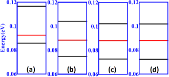
According to the calculation for a typical 3200-atom supercell [see Figure 2(a_1)],
the three levels introduced by Mn in the bulk GaAs gap
are found to be spread over an energy interval of approximately meV,
when SOI is included in the calculation [note that in Figure 2(a_1),
the top-most and the lowest levels in the gap are split by meV].
Figure 3 shows similar calculations for different supercell sizes.
As one can see from the figure, the position of the three levels in the gap starts to shift
as the supercell size is increased, gradually approaching saturation as a function of the size
(the absolute position of the
levels does not change appreciably for clusters containing more than 20,000 atoms).
However, the splitting
between the levels as well as the relative position of the acceptor level with respect to the top of valance
band remains unchanged (113 meV).
This is a shortcoming that the present quantum-spin model shares with
the classical-spin models introduced in [18] and [22].
In fact the three levels of predominantly
-character, appearing in the gap, should be degenerate
in the perfectly tetragonal environment of an impurity in bulk GaAs [29]. The lifting of the
degeneracy is most likely related to the breaking of rotational symmetry
due to the essentially mean-field nature of the approximation for the exchange coupling between
the TM impurity -levels and the -levels of the nearest neighbor As atoms,
used in both the quantum- and the classical-spin model. Note that the same problem occurs in the DFT calculations,
which are also based on a broken-symmetry approach.
In contrast to this, a perfectly three-fold degenerate level is expected for the
present model as well as for the classical spin model [18, 22],
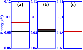
when SOI is switched off. We confirm this by calculating the in-gap level structure for Mn in the bulk in the absence of
SOI. We find that the splitting between the levels reduces from 11.54 meV
for a 3200-atom to 0.62 meV for a 20,000-atom cluster (Figure 4). That is,
in the absence of SOI the splitting between the three Mn-induced levels in the bulk GaAs gap
is zero for this model.
To summarize, our calculations show that
(i) in the presence of SOI the splitting between the three levels in the gap, as well as the
relative position of the acceptor level with respect to the top
of the valence band (113 meV) remain unchanged even for very large clusters
containing up to 30,000 atoms (Figure 3), and
(ii) in the absence of SOI the small splitting between the levels,
which is still present in calculations for a 3200-atom supercell, is
purely due to a finite-size effect and
quickly vanishes with increasing the
size of the supercell (Figure 4).
We will now focus on the calculations of magnetic anisotropy energy for
a single Mn in the bulk and on the (110) surface of GaAs.
In particular, we will discuss the trend of magnetic anisotropy with increasing
the size of the supercell.
In order to evaluate the magnetic anisotropy of the system, one should in principle
calculate the entire eigen-spectrum of the Hamiltonian.
However, for larger clusters we are forced to use the Lanczos diagonalization method
that allows us to obtain eigenvalues (and eigenvectors) of the Hamiltonian only
in a very small window around the Fermi level (or around the position of the acceptor level in the gap).
In the case of the classical-spin model [22] one can overcome
this difficulty by using the following important property of the system.
It can be shown that the
energy of the (single-particle) acceptor level
and the (many-particle) ground state (GS)
energy of the system are very accurately related by the following expression
| (6) |
where is a constant independent of and . This means that the sum of the two energies and is the same for any direction of the Mn magnetic moment. If and define the two directions where attains its maximum and minimum value respectively, from Equation 6 we obtain
The quantity is by definition the magnetic anisotropy energy () of the system. Similarly, Equation 6 implies that is the opposite of the magnetic anisotropy of the acceptor level, . Therefore, we can rewrite Equation 3 as
| (7) |
Equations 6 and 7 contain a very strong physical result and are particularly
useful for practical calculations of the magnetic anisotropy energy for large clusters, namely
they imply that the total anisotropy
of the system is essentially determined by the anisotropy of the single-particle acceptor level.
This picture remains valid as long as the coupling to the conduction band is not sensitive
to the magnetization orientation.
In contrast to the classical-spin model, the results of the calculations of magnetic anisotropy energy
using the quantum-spin model indicate that
Equation 6 is, in principle, not satisfied.
As a result, the quantity is not exactly zero in our calculations, however
its value is negligibly small.
We suggest that this small change in the difference between the GS and the acceptor
anisotropy energies is due to the inclusion of the -orbitals, which
brings about a magnetization-direction dependent coupling with the conduction band.
In the classical-spin model, the polarized spins of the majority
-electrons are represented by a classical vector with a fixed
magnitude of . This only affects the (occupied)
energy-levels of the valence band through its SOI-induced orientation
dependence. In contrast, our quantum-spin model includes the impurity
-orbitals and the corresponding hopping amplitudes between the
-orbitals and the nearest neighbor As atoms explicitly in the
Hamiltonian. Unoccupied minority -levels, located way up in the
conduction band, hybridize with like-spin As -orbitals of the
valence band. This coupling is responsible for the small deviation
from Equation 7, which is also affected by the distance of the Mn atom from
the surface. The fact that the deviation from the classical-spin model
result is so small indicates that the effect of the conduction
band hopping in this system is not very important.
In Figure 5 we present the calculated magnetic anisotropy energy for the Mn acceptor in the bulk,
for very large clusters containing up to approximately 34,000 atoms.
These calculations show explicitly that the bulk magnetic anisotropy energy decreases
with increasing the cluster size, dropping drops from 3.7 meV for a 3200-atom cluster to
the very small value of 0.09 meV for a cluster containing 34,000 atoms.
The inset in Figure 5 shows that the magnetic anisotropy energy decreases linearly with the inverse
number of atoms in the cluster.
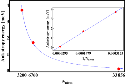
Figure 6 shows the calculated magnetic anisotropy energy of the system as
a function of the Mn depth, for two different cases: (i) a 3200-atom supercell with
19 Ga layers along the [110] direction, and (ii) a 6760-atom supercell with
25 Ga layers. In case (i), when the system size is still suitable for
full diagonalization, we performed systematic comparison between exact calculation
of MAE, based on the entire eigen-spectrum of the Hamiltonian, and the Lanczos result,
obtained by calculating the acceptor anisotropy, MAEacc. We find that the two sets
of calculations, in particular the value of the magnetic anisotropy energy for bulk, surface and subsurfaces,
are in good agreement with each other and with the results of the classical-spin model [22, 27].
This suggest that the deviations from Equation 7 are indeed small even when the -levels of the impurity are
included explicitly in the Hamiltonian.
The only discrepancy is found in the magnetic anisotropy landscapes, calculated for the surface and the first sublayer, which
will be discussed later in the text. In case (ii) the full diagonalization results are no longer available and
we rely solely on the calculations of MAEacc. Note that for a 3200-atom cluster, the 9-th sublayer
corresponds to the center of the cluster and the Mn atom can not be positioned any further away from the surface.
However, for a 6760-atom cluster, we are able to perform calculations for Mn in sublayers 1 to 12 below the surface.
This enables us to draw more general conclusions on the trend of magnetic anisotropy for Mn positioned in the sublayers.
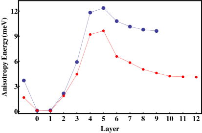
We will now discuss some of the key features of the magnetic anisotropy calculations for Mn positioned in the sublayers
(Figure 6). For both cluster sizes considered here,
the anisotropy energy increases as Mn is moved down to the fifth sublayer
and it decreases for Mn positioned deeper below the surface. This peculiar behavior
has been reported previously in calculations based on the classical-spin model [22, 27].
It can be explained based on the following arguments.
A very small magnetic anisotropy of the surface layer (0.11 meV) and first
sublayer (0.06 meV) is due to the highly localized
and less anisotropic character of the acceptor wavefunction, compared to
the acceptor in other sublayers [27] [Panels (a) and (b) of Figure 8].
As the impurity is moved away from the first sublayer, the wavefunction of the corresponding acceptor
state becomes more extended [22, 27] and will be therefore
strongly affected by the surface, until the Mn atom is moved
deep enough so that the surface effects become negligible (this situation corresponds to the sixth sublayer).
Furthermore, we point out another important feature of Figure 6,
which has not been discussed previously and
partly motivates the calculations for larger clusters. As the Mn impurity is moved down towards the center of the cluster,
one would expect the anisotropy energy to decrease until it reaches its bulk value,
when Mn is placed in the center of the cluster. Based on the calculation for a relatively small 3200-atom supercell
(blue curve in Figure 6), it is not clear whether this is indeed the case. In this calculation, not only the bulk
anisotropy energy is non negligible (3.7 meV) but also the anisotropy for Mn in the 9th sublayer is quite large (9 meV).
This issue is clarified by the calculation for a larger cluster containing 6760 atoms
(red curve in Figure 6). Firstly, the
maximum value of the magnetic anisotropy energy, which occurs for the Mn in the fifth sublayer, decreases compared to the smaller cluster, which
is also consistent with the bulk calculations (Figure 5). Secondly,
the anisotropy energy decreases even further as Mn is moved away from the surface
beyond the 9-th sublayer. These observations confirm the trend towards saturation of the
magnetic anisotropy energy to its bulk value, as the impurity is positioned in deeper sublayers.
We would like to add a remark about the trend of the anisotropy
energy as a function of cluster size. When Mn is placed in the
middle of the cluster in the bulk calculation, the distance between
the two Mn atoms in the neighboring supercells and, as a result,
the overlap between their wavefunctions depend on the size of
the supercell. With increasing the size of the cluster, the Mn
wavefunction will eventually approach that of an isolated impurity
and, as a result of perfect tetragonal symmetry, its MAE drops to a
value very close to zero (exactly zero in the limit of an infinitely
large cluster). In the case of Mn placed in the sublayers, as long
as it is not very far from the surface (for example, in the fifth
sublayer), the situation is different from the bulk. Increasing
the size of the supercell does finally detach the Mn wavefunction
from the boundary planes perpendicular to (110) surface. However,
the Mn-acceptor wavefunction along the [110] direction will still
be influenced by the lower symmetry of (110) surface. No matter
how large the supercell is, the MAE of Mn in the sublayers (say,
in the fifth sublayer) will not vanish as long as this sublayer
remains close enough to the surface. Indeed, our new set of calculations
for a cluster containing more than 55,000 atoms with 54 Ga layers
along the [110] direction confirmed our prediction. Due to
computationally-demanding and time-consuming nature of these
calculations, we were not able to rotate the quantization axis for
all possible directions to plot a figure like
Figure 7. Instead, we chose two
specific directions, known to be the easy and the hard directions,
for sublayers number 5 and 26. Note that, the 26 sublayer is the
deepest sublayer for this cluster. Therefore, its magnetic anisotropy
landscape should resemble the 12th sublayer of a 6760-atoms cluster,
shown in Figure 7, or the 9th sublayer of a 3200-atoms
cluster, shown in Figure 9 of the reference [22]. (We assume that the
anisotropy landscape will not change qualitatively with increasing the
cluster size, therefore the easy and hard directions will be the same).
In these new calculations, we find that the anisotropy energy between
the easy and hard directions for the 5th sublayer is slightly smaller
(9.1 meV) than value found for a smaller cluster (9.6 meV from Figure 6).
However, for the 26th sublayer, the anisotropy energy is only 0.05 meV
(compare to 4.1 meV for the sublayer in the middle of 6760-atoms cluster (12th)).
These calculations further confirm that the wavefunction of the Mn atom
placed in the middle of a very large cluster will be highly isolated from
all boundaries and its anisotropy energy will drop to zero, while for the
sublayers close to the surface it will remain anisotropic.
Figure 7 shows the acceptor magnetic anisotropy landscape
for Mn near the (110) GaAs surface, calculated for a 6760-atom cluster. Here
the magnetic anisotropy energy is plotted for different directions of the
Mn spin quantization axis, characterized by angles and . According to
previous calculations [27], for the directions considered here (, ),
the impurity magnetic moment has one easy and one hard axis.
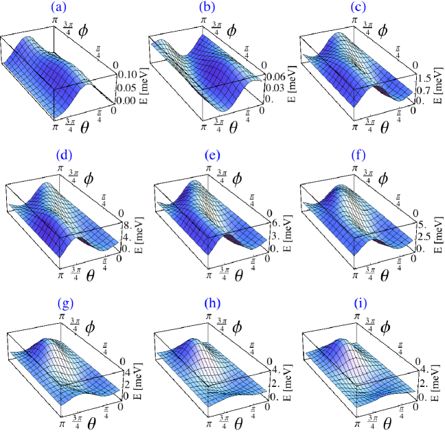
The overall pattern
of the magnetic anisotropy landscape for this cluster size closely resembles
the previous calculations for smaller clusters [27], with only two exceptions.
The anisotropy landscapes (but not the absolute value of the magnetic anisotropy energy)
for Mn on the surface and in the first sublayer [Figure 7(a) and (b)]
is different from those reported in [27].
As explained earlier, in the present model, which includes explicitly the
-levels of the impurity atom, the magnetic anisotropy energy of the system
is not necessarily equal (in absolute value) to the
anisotropy of the single-particle
acceptor level. In particular, if the anisotropy energy itself is small, which
is indeed the case for the surface and the first sublayer, the difference
between MAE and MAEacc can become visible for different direction of
the impurity magnetic moment. In fact, we carefully compared
the acceptor and the GS anisotropy landscapes in all sublayers
for the smaller cluster size. We find that the difference is indeed most visible
for Mn on the surface and in the first sublayer, which further supports our
calculations for the larger cluster, where calculations of the GS anisotropy are
not possible.
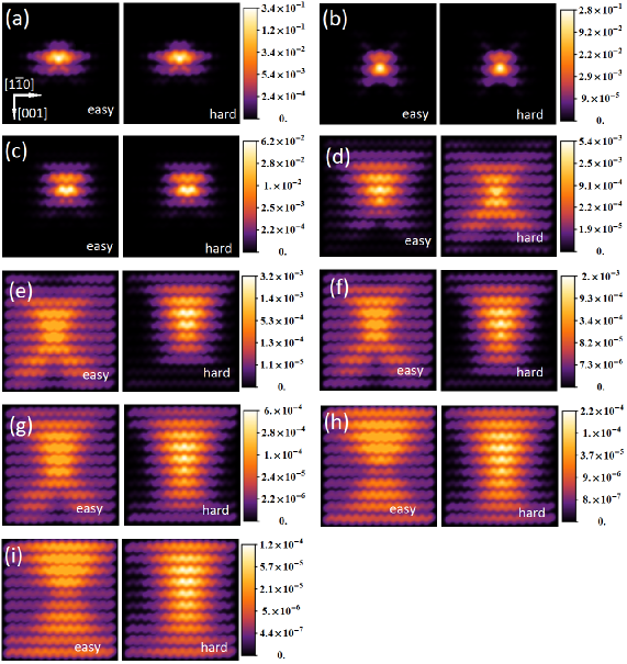
In order to be able to address STM topographies of the Mn acceptor, when Mn is placed on the surface or sublayers of GaAs (110) surface, we plotted the corresponding LDOS in Figure 8. In agreement with previous theoretical and experimental works [21, 22, 41, 27], we observed the following properties in the LDOS. All images show a mirror plane as reported previously. The LDOS extends spatially even further along the [001] direction, for the case in which Mn is placed in deeper sublayers [41, 22]. The deeper the Mn is from the (110) surface, the more symmetric the anisotropic features introduced by Mn becomes, which is an indication that the environment for this Mn depth is more resembling the bulk host material. Using larger clusters, we were able to position the impurity as deep as in the 12th sublayer. As one can see from the last two panels of Figure 8, the symmetric butterfly shape becomes more pronounced in 11th and 12th sublayers [41, 22]. The acceptor-LDOS in deeper sublayers show a triangular shape, which shifts to a butterfly shape with stronger upper-wing as Mn moves deeper. This has been described to be related to the intrinsic strain associated with the buckling relaxation [21]. The increase in the intensity along the hard axis compared to the easy axis after the fifth sublayer has been observed and explained previously [22]. The more pronounced LDOS for the deeper sublayers compared to previous results is due to the smaller magnetic anisotropy barrier between the easy and hard axes. The deep acceptor for Mn on the surface and in the first sublayer results in highly localized LDOS, as seen in Figure 8 (a) and (b), respectively. As the Mn atom is moved down towards the center of the cluster, its binding energy decreases and the associated wavefunction is less localized [see Figure 8 (c)-(i)]. Note that, although the shape of the acceptor LDOS in the second sublayer [Figure 8 (c)] appears to be less extended compared to subsequent layers, only 10% of the spectral weight is located on the Mn atom, indicating a more delocalized acceptor wavefunction compared to the surface and the first sublayer. Finally, due to the larger size of the cluster, one can see that the wavefunction for localized cases is completely detached from the boundary planes perpendicular to the (110) plane.
4 Conclusions
In this paper we have investigated the in-gap electronic structure
and the magnetic anisotropy energy of a
single Mn acceptor in bulk and near the (110) surface of GaAs,
using a fully-microscopic TB model with supercells
containing up to atoms.
The main outstanding issue addressed in our calculations has been
the effect of the finite supercell size on the
degeneracy of the impurity-induced energy levels in the bulk GaAs with and
without SOI, and on the behavior of the magnetic anisotropy
energy as a function of the Mn depth from the surface.
We found that in the absence of SOI, the three acceptor energy levels,
introduced by the Mn dopant in the bulk GaAs gap, become degenerate with
increasing the cluster size, which is expected from symmetry arguments.
However, in the presence of SOI, the finite splitting between the levels, which is
of the order of 30 meV, remains unchanged with increasing the cluster size
up to atoms. We attribute this effect to the
shortcomings of the mean-field treatment of the exchange coupling between
the Mn impurity spin and its nearest neighbor As atoms.
The calculations of the magnetic anisotropy energy for Mn in bulk and near the surface
revealed a number of important features, which have not been investigated previously.
In particular, we showed for the first time that the non-negligible anisotropy of the
Mn dopant in the bulk, found in earlier calculations, is due to a finite-size effect
and that it indeed vanishes with increasing the size of the supercell.
We also found that the magnetic anisotropy for Mn near the surface decreases
considerably for larger clusters. A clear tendency of the surface anisotropy towards
the bulk value was observed, as the dopant was moved away from the surface.
In addition, based on the calculations of magnetic anisotropy,
we identified some important differences between the present treatment, which takes
into account the impurity -levels, and the classical-spin model, which
treats them as an effective classical spin. It was shown that, in the former case
the robust relationship between the ground states anisotropy and
the acceptor anisotropy no longer holds, due to the explicit inclusion of the impurity
-levels in the Hamiltonian.
In conclusion, our calculations provide an accurate and detailed picture of the electronic structure, LDOS
and magnetic anisotropy for a single Mn dopant, positioned in the vicinity of the (110) GaAs surface.
We anticipate that these result will be important for interpreting the on-going STM experiments on this and other
similar TM-impurity systems, and in particular for on-going experimental efforts to
manipulate the Mn acceptor states by means of external electric and magnetic fields.
A reliable estimate of the magnetic anisotropy landscape for individual TM dopants close to the surface, like the one
presented here, is also essential to extract an effective spin Hamiltonian for the impurity spin, following
for example the procedure put forward in reference [24].
Effective spin Hamiltonians for solitary TM dopants in a semiconductor host can be used to model magnetic excitations,
which are probed in spin inelastic electron tunneling spectroscopy[42].
References
References
- [1] Koenraad P M and Flatté M E 2011 Nat. Mater. 10 91
- [2] Hirjibehedin C F, Lutz C P and Heinrich A 2006 Science 312 1021
- [3] Kitchen D, Richardella A, Tang J M, Flatté M E and Yazdani A 2006 Nature 442 436
- [4] Yakunin A M, Silov A Y, Koenraad P M, Roy W V, Boeck J D, Tang J M and Flatté M E 2004 Phys. Rev. Lett 92 216806
- [5] Shinada T, Okamoto S, Kobayashi T and Ohdomari I 2005 Nature (London) 437 1128
- [6] Marczinowski F, Wiebe J, Tang J M, Flatté M E, Maier F, Morgenstern M and Wiesendager R 2007 Phys. Rev. Lett. 99 157202
- [7] Garleff J K, Çelebi C, van Roy W, Tang J M, Flatté M E and Koenraad P M 2008 Phys. Rev. B 78 075313
- [8] Lee D H and Gupta J A 2010 Science 330 1807
- [9] Garleff J K, Wijnheijmer A P, Silov A Y, van Bree J, Roy W V, Tang J M, Flatté M E and Koenraad P M 2010 Phys. Rev. B 82 035303
- [10] Fuechsle M, Miwa J A, Mahapatra S, Ryu H, Lee S, Warschkow O, Hollenberg L C L, Klimeck G and Simmons M Y 2012 Nat. Nanotechnol. 7 242
- [11] Pla J J, Tan K Y, Dehollain J P, Lim W H, Morton J, Jamieson D N, Dzurak A S and Morello A 2012 Nature (London) 489 541
- [12] Zhao Y, Mahadevan P and Zunger A 2004 Apl. Phys. Lett. 19 3753
- [13] Mahadevan P, Zunger A and Sarma D D 2004 Phys. Rev. Lett. 93 177201
- [14] Mikkelsen A, Sanyal B, Sadowski J, Ouattara L, Kanski J, Mirbt S, Eriksson O and Lundgren E 2004 Phys. Rev. B 70(8) 085411
- [15] Stroppa A, Duan X, Peressi M, Furlanetto D and Modesti S 2007 Phys. Rev. B 75(19) 195335
- [16] Ebert H and Mankovsky S 2009 Phys. Rev. B 79 045209
- [17] Islam M F and Canali C M 2012 Phys. Rev. B 85 155306
- [18] Tang J M and Flatté M E 2004 Phys. Rev. Lett. 92 047201
- [19] Tang J M and Flatté M E 2005 Phys. Rev. B 72 161315
- [20] Timm C and MacDonald A H 2005 Phys. Rev. B 71 155206
- [21] Jancu J M, Girard J C, Nestoklon M O, Lemaitre A, Glas F, Wang Z Z and Voisin P 2008 Physical Review Letters 101 196801
- [22] Strandberg T O, Canali C M and MacDonald A H 2009 Phys. Rev. B 80 024425
- [23] Strandberg T O, Canali C M and MacDonald A H 2010 Phys. Rev. B 81 054401
- [24] Strandberg T O, Canali C M and MacDonald A H 2011 Phys. Rev. Lett. 106 017202
- [25] Mašek J, Máca F, Kudrnovský J, Makarovsky O, Eaves L, Campion R P, Edmonds K W, Rushforth A W, Foxon C T, Gallagher B L, Novák V, Sinova J and Jungwirth T 2010 Phys. Rev. Lett. 105(22) 227202
- [26] Bozkurt M, Mahani M R, Studer P, Tang J M, Schofield S R, Curson N J, Flatté M E, Silov A Y, Hirjibehedin C F, Canali C M and Koenraad P M 2013 Phys. Rev. B 88(20) 205203
- [27] Mahani M, Islam M F, Pertsova A and Canali C 2014 arXiv:1401.0703
- [28] Hamers R J and Padowitz D F 2001 Scanning probe microscopy and spectroscopy: theory, techniques and applications (New York: Wiley)
- [29] Subramanian H and Han J E 2013 J. Phys.: Condens. Matter 25 206005
- [30] Chadi D J 1977 Phys. Rev. B 16 790
- [31] Slater J C and Koster G F 1954 Phys. Rev. 94 1498
- [32] Papaconstantopoulos D A and Mehl M J 2003 J. Phys.: Cond. Mat. 15 R413
- [33] Jancu J M, Scholz R, Beltram F and Bassani F 1998 Phys. Rev. B 57 6493
- [34] Chadi D J 1978 Phys. Rev. Lett. 41 1062
- [35] Chadi D J 1979 Phys. Rev. B 19 2074
- [36] MATLAB 2010 version 7.10.0 (R2010a) (Natick, Massachusetts: The MathWorks Inc.)
- [37] Schairer W and Schmidt M 1974 Phys. Rev. B 10 2501
- [38] Lee T and Anderson W W 1964 Solid State Commun. 2 265
- [39] Chapman R A and Hutchinson W G 1967 Phys. Rev. Lett. 18 443
- [40] Linnarsson M, Janzen E, Monemar B, Kleverman M and Thilderkvist A 1997 Phys. Rev. B 55 6938
- [41] Çelebi C, Koenraad P M, Silov A Y, Van Roy W, Monakhov A M, Tang J M and Flatté M E 2008 Phys. Rev. B 77(7) 075328
- [42] Khajetoorians A A, Chilian B, Wiebe J, Schuwalow S, Lechermann F and Wiesendanger R 2010 Nature 467 1084