Sub-nanometer flattening of a 45-cm long, 45-actuator x-ray deformable mirror
Abstract
We have built a 45-cm long x-ray deformable mirror of super-polished single-crystal silicon that has 45 actuators along the tangential axis. After assembly the surface height error was 19 nm rms. With use of high-precision visible-light metrology and precise control algorithms, we have actuated the x-ray deformable mirror and flattened its entire surface to 0.7 nm rms controllable figure error. This is, to our knowledge, the first sub-nanometer active flattening of a substrate longer than 15 cm.
pacs:
220.1080, 340.7470, 120.4640, 230.4040I Introduction
The advent of 4th-generation x-ray light sources (i.e., free electron lasers like the Linac Coherent Light Source in the U.S. and SPring-8 Angstrom Compact free electron laser in Japan and advanced synchrotrons like the National Synchrotron Light Source II in the U.S.) requires increasingly advanced and high-performance x-ray mirrors. Combining expertise in visible wavelength adaptive optics and reflective x-ray optics, Lawrence Livermore National Laboratory (LLNL) has begun a research and development effort to design, fabricate and test x-ray deformable mirrors.
X-ray deformable mirrors could provide two significant benefits over traditional non-adaptive x-ray optics. First, active control is a potentially inexpensive way to achieve better surface figure than is possible by polishing alone, particularly on long substrates. Secondly, the ability to change the figure allows for dynamic correction of aberrations in a x-ray beam line. This includes both self-correction of errors in the mirror itself (such as those caused by thermal loading) and correction of errors on other optics, the latter of which has been demonstrated elsewhereMimura2010Breaking-the-10 .
With these goals in mind we have built a 45-cm x-ray deformable mirror (XDM). As detailed below, this mirror was designed to provide fine-scale control of its surface. Using precise visible-wavelength metrology, we have been able to generate voltage commands for the XDM’s actuators that flatten it to as good as 0.7 nm rms, which is significantly better than the initial substrate polishing before assembly. The following sections describe the XDM, the metrology equipment, our calibration and control methods and finally the flattening results.
To place our XDM in context, we must consider two types of mirrors that have been developed by others in the field. The first is with non-active super-polished mirrors. We need to be able to control our XDM to a comparable flatness. Our XDM was designed with the same size specifications as the hard x-ray offset mirrors (known as HOMS) for LCLS doi:10.1117/12.795912 ; Barty2009Predicting-the- . Visible-light metrology (using the same interferometer that we have used for this work) on the four delivered HOMS measured the figure errors (which exclude cylinder) between 1.0 and 2.4 nm rms doi:10.1117/12.795912 ; Barty2009Predicting-the- . JTEC produces mirrors up to 50 cm long, with a claimed shape error of less than 0.5 nm rms at best effort JTECwebsite .
Although fixed figure 0.5 m flats with 0.5 nm rms error are being produced, the advantages of a variable figure capable 0.5 nm figure error tolerance motivate this study. For example, a variable figure mirror can compensate for localized heating that drives figure error well above the as manufactured specification. If mirrors are coated, a concomitant cylinder can be compensated. Finally, a deformable mirror may aid in compensating figure errors introduced by final focusing optics, which are not yet being manufactured to diffraction limited performance. One deformable mirror can correct the net sum of all these effects, without the need to fully understanding the origin of each component.
The second point of comparison for our XDM is to other deformable x-ray optics. Below, we summarize published performance of the best flattening achieved for other deformable x-ray mirrors. In 2010 a French collaboration Mercere2010Hartmann-wavefr developed an active x-ray mirror to be deployed at the SOLEIL facility; this mirror implements a 35 4 0.8 cm silicon substrate held between an active jaw and a flexor, to generate variable elliptical profiles. In addition the mirror features 10 actuators across its length to minimize asphere. The actuators are perpendicular to the mirror surface, and force is applied by a spring-floating head coupled to a stepper motor. Actuator hysteresis was reported to be 0.1. The SOLEIL team demonstrated flattening of the mirror down to 3.0 nm rms of asphere, and 0.6rad slope errors over 30 cm of clear aperture, with a maximum radius of curvature equal to 60 m.
In the same year, the Diamond Light Source developed a 15 4.5 cm adaptive x-ray mirror, including eight piezo bimorph actuators Sawhney2010A-novel-adaptiv . This mirror was specifically designed to achieve a high level of figure control, while allowing for adjustable radius of curvature. The actuated mirror, built by SESO and super polished by JTECH via Elastic Emission Machining (EEM), reached 0.66 nm rms of asphere over 12 cm of clear aperture, with the smallest beam size at focus equal to 1.2 m FWHM.
Another x-ray deformable mirror was developed in Japan and deployed at SPring-8 before a pair of Kirkpatrick-Baez (KB) mirrors, to achieve nearly diffraction-limited beam focusing Mimura2010An-adaptive-opt . The 12 cm silicon substrate was super-polished by EEM, and features 16 piezoelectric plates. During operation, a Fizeau interferometer was placed in front of the mirror to provide real time figure correction. The experimental team reported a 7 nm FWHM spot size at the focus plane. For this experiment an estimated 10 nm peak-to-valley surface profile was found in situ, but several error sources were listed. Previously, visible light metrology on this optic Kimura2008Development-of- outside of the beam line was conducted with Fizeau interferometry. An approximately 2 nm peak-to-valley figure error was measured at best flat. No rms figure error was reported; for a typical figure error PSD this is approximately 0.7 nm rms.
In 2012 the x-ray optic group at the Elettra Synchrotron facility in Italy reported on the successful construction of an adaptive x-ray mirror for the TIMEX beamline at FERMI doi:10.1117/12.929701 . This mirror is 40 cm long and 4 cm wide, and features 13 piezo actuators and 13 strain gauges. Rough flattening of the mirror is first achieved by acting on four clamps located on the mirror mount. The idea of including calibrated strain gauges in the design allows the mirror to work in closed loop without the need of a wavefront sensor. The same idea was implemented for the design of our XDM. To our knowledge no precision flattening results have been reported from Elettra.
II Deformable mirror design
Our single crystal silicon substrate is 45 cm in length, 3 cm high, and 4 cm in width. Substrate quality is discussed in Section IV. The mirror and actuators are supported on an invar mount, and enclosed in a protective housing that leaves the reflective surface exposed to grazing incidence x-rays. The substrate was cut from a large boule similar to those typically used in wafer fabrication, which are usually pulled in the (111) direction. Typical resistivity is 10 ohm-cm. Neither parameter has any significant affect on our mirror’s performance. As of now we do not expect to deposit any single or multilayer coating on the silicon substrate. Preliminary experiments at a synchrotron facility will be conducted at low photon energy and grazing incidence, well within the critical angle of silicon.
Figure 1 illustrates how the 45 actuators are bonded on the side opposite the reflective surface.
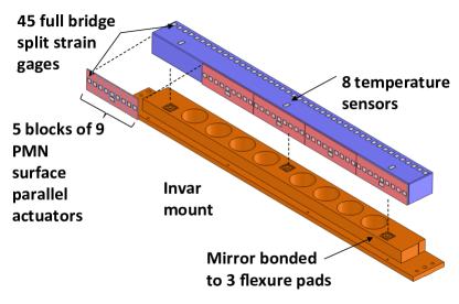
Each actuator is 1 cm long, 3 cm high, and about 0.15 cm thick. They are spaced evenly every 1 cm along the tangential axis of the mirror. The surface parallel actuator geometry of the actuators, along with three flexure supports machined into the Invar mount, minimize unintended forces on the mirror, and their effect on figure during actuation. The actuators are epoxy bonded to the mirror while at mid-range of their operating voltage, which enables the mirror to bend both concave and convex. The mirror is bonded to the three flexure pads to constrain all motion except that induced by the actuators. The flexures also isolate the mirror from differential thermal expansion between the substrate and mount.
The actuators operate from 15 to 75 volts. The actuators were bonded to the substrate at 45 V. This enables the XDM to make spherical surface in either direction from a nominal flat surface. The voltage at which the mirror has no curvature, nominally 45 V, is referred to as the bias voltage.
Figure 1 also illustrates the location of 45 full bridge strain gauges. One half of each bridge is bonded to the back side of each actuator. The mating half-bridge is bonded to the top of the mirror, where strain is similar to that at the mirror’s reflecting surface. The strain resolution of each gauge is about 10 parts per billion (commonly referred to as nanostrain). This corresponds to each gauge measuring surface figure changes to better than 1 nm between gauges.
The strain gauges can detect and correct for differential expansion between the mirror and actuators. However, because the gauge response itself may be slightly temperature sensitive, Resistance Temperature Detectors (RTDs) are bonded to the mirror to measure temperature: three on the top of the mirror, and one to each of the five Lead Magnesium Niobate (PbMnNb or PMN) actuator blocks. The eight RTD locations are also shown in Figure 1.
The mirror’s actuators, strain gauges, and RTD’s are all wired to a printed circuit board that is secured to the back of the mirror mount. Each wire from the mirror is soldered to the printed circuit board. Electrical connectors embedded in the board connect the mirror assembly to power supplies and signal processors. The circuit board, mirror, and mount after assembly are enclosed, with cables required for operation connected to the back.
Currently the mirror is compatible with operations in vacuum limited to mbar; this should offer enough flexibility in terms of mirror deployment, especially considering that we can always take advantage of differential pumping, if an ultra-high vacuum environment is needed. Also, we do not expect appreciable temperature changes on the mirror as a consequence of x-ray heat load, since the shallow grazing incidence design of the optic guarantees a large footprint of the x-ray spot.
In order to provide very high quality strain gauge readings, while also keeping costs in line, the 45 strain gauge signals coming off the XDM printed circuit board are multiplexed into a single channel of an MGCplus measurement system (HBM, Inc). The MGCplus is outfitted with an ML38B amplifier and conditioning module. The signals are multiplexed using an Agilent 34980A data acquisition box with three 34922A multiplexer modules. Although cost and simplicity are benefits of this approach, a detriment is that we need to wait a considerable amount of time between strain gauge readings to let a long time constant low-pass filter settle each time the multiplexer is switched. At present, we wait 20 seconds between reading each strain gauge, for a total of 15 minutes for all 45 gauges. The 8 RTDs are multiplexed through the same Agilent 34980A and read with an Agilent 34411A DMM. Much less conditioning is required for the RTDs and, hence, they can be read almost instantaneously after a multiplexer switch. The 45 actuators are controlled using Northrup Grumman USB DM drive electronics. All of these electronics are connected to the control computer over serial channels. For ease of development and flexibility during testing, Matlab was selected as the software development environment. Software developed by the team provides the control, measurement, and analysis capabilities needed to support the work described herein.
Though we do not use the strain gauges and RTDs in the work described here, we describe them for completeness. These sensors were included to help us control the XDM’s stability through time and with temperature changes, which is a subject for future work. We next discuss the visible light metrology that we use to characterize the XDM.
III Visible-light metrology
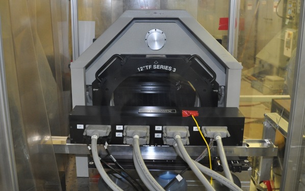
III.1 The 12-inch Zygo interferometer
The Zygo Mark II phasing interferometer used in this work has a noise floor of about 0.3 nm, and is calibrated to measure figure with an absolute accuracy approaching 1 nm (rms) over the 28 cm field of view. The 45 cm deformable mirror figure is constructed by stitching three 28 cm long interferograms. Without suitable characterization, interferometer calibration errors will produce inconsistencies within stitched regions, limiting the ability to demonstrate deformable mirror performance.
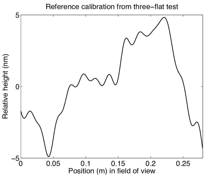
Therefore a three flat test was used to calibrate the interferometer. During the test two transmission flats, T1 and T2, are mounted onto the interferometer, and also placed at the optic under test location. The third optic is a reflection flat labeled R. It is placed at the optic under test location, and is rotatable 180 degrees about its optic axis. The figure of each optic along a horizontal line can be calculated from the three data files, and the solution for T2 is used as the reference calibration when measuring our XDM. This reference calibration is shown in Figure 2. This amplitude of the correction is nm, significantly more than the signal that we want to measure at best flat.
This study required over a hundred surface figure measurements per day during the course of algorithm optimization. This measurement rate would best be met with a full aperture visible light interferometer. However, the 600 mm aperture interferometers tested had a measurement noise floor well above the 0.1 nm noise floor of our best performing 300 mm aperture unit. Off-normal incidence angles with additional reflectors were tested using the 300 mm unit, but the additional air path length severely increased the intrinsic instrument noise. As a result, the 300 mm unit at normal incidence was selected, and stitching employed to measure the full aperture. The performance of this method in measuring 450 mm mirrors compared favorably with long trace profile measurements made at LBL doi:10.1117/12.945915 , as well as in-situ measurement made at x-ray wavelengths at LCLS Rutishauser2012Exploring-the-w .
III.2 Mounting and measuring the XDM
As noted above, we take three measurements of the XDM surface and stitch them together. The mirror’s three positions in front of the interferometer are termed right, center and left. The right position corresponds to the lowest numbered actuators on the XDM. The center position is approximately centered on actuator 23. The left position corresponds to the higher numbered actuators on the XDM. This three-measurement setup provides 20 cm overlap in the two stitching zones.
The centerline of the XDM is matched to the calibrated horizontal line of the interferometer. The mount is moved from right to center to left with no vertical motion to ensure the interferometer is measuring the mirror at the same elevation. The mount is designed with stops to ensure repeatability of better than 1 mm (which is one pixel in the interferometer, see below) as it is moved.
Interferometer measurements are mapped to the physical surface of the XDM by adjusting interferometer magnification to 1 mm of mirror surface/pixel. Each measurement is 288 pixels long, corresponding to 28.8 cm on the XDM surface. We define an x-axis along the centerline of the XDM, with at actuator 23. In each of the three positions different actuators are bent and measurements are taken to determine the exact portion of the XDM that the interferometer measures. At present, in the right position the measurement spans -22.2 to 6.5 cm along the x axis (as defined above); in center position it spans -14.1 to 14.6 cm; in left position it spans -6.6 to 22.1 cm.
Calibration accuracy is essential for stitching interferograms. The interferometer calibration file is subtracted from each measurement to yield the absolute height of the XDM. Then piston (constant height) and tilt (linear height) are removed from each measurement. Then, ignoring the fifty pixels at either end of the measurements, we align the remaining overlap between the right and center measurements. This alignment is done by adjusting the tilt and piston on the right measurement to produce the minimum squared error between it and the center measurement in the overlap region. Then we repeat the procedure to align the left measurement to the center, again minimizing the squared error. The results of such an alignment are shown in Figure 3.
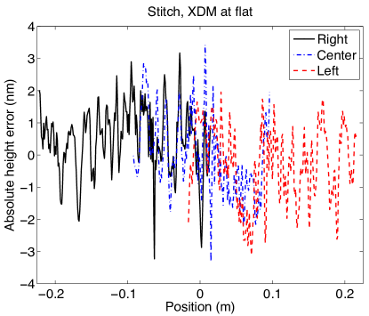
The excellent agreement of the three measurements verifies the quality of the calibration via the three-flat test. The final stitched measurement is produced by taking the mean of all valid sample points (from either one, two or three positions) for each x location. Points at the ends of the lineouts are ignored if they display artifacts of miscalibration. The resulting stitched measurement is always absolute height.
A stitched measurement represents nearly the entire 45-cm length of the XDM. Figure 3 shows very good agreement between the different views of the same mirror shape, for there measurements taken with the mirror held at a fixed voltage (from one of the flattening experiments, see Section VI.2). Since the calibration by the three-flat test is nm (see Figure 2) this excellent agreement gives us confidence that the calibration is correct. All claims about figure error are made relative to this calibration. Of course, the calibration may be slightly wrong, and hence the flattening not quite as flat. However all external metrology, whether of deformable or static x-ray optics, will require calibration. If when testing at a x-ray light source our best flat produces an x-ray beam of lower than expected quality, we will be able to change the voltages commanding it to improve the figure, dependent accurate calibration of any in situ metrology.
Also apparent in Figure 3 is that there is significant high-spatial frequency content in the interferometer measurements. Though some of this may represent high-frequency polishing errors on the XDM, most of it is noise. In the literature doi:10.1117/12.795912 ; Sawhney2010A-novel-adaptiv such noisy measurements are usually low-passor median filtered.
The fundamental limits of phasing interferometer noise are discussed in Sommargren2002100-picometer-i . The noise floor of our measurements correspond to about 632 nm/1000, which is found by many researchers Malacara1992Optical-Shop-Te to be the performance limit for commercially available equipment. This performance is only achieved when environment vibration and air turbulence are fully suppressed, leaving only the intrinsic noise of the measurement machine. If there were a single cause to this floor, it could be addressed and corrected by interferometer manufacturers.
In our case we have a natural characteristic frequency for the system that is set by the XDM. Since the actuators are spaced every one centimeter, the highest controllable mode has a period of two centimeters. The XDM cannot make shapes of higher spatial frequency. When assessing the performance of our flattening, we only consider the spatial frequencies below this cutoff. To obtain this portion of the signal, we simply low-pass filter the measurement with a hard cutoff in our software. We term such a filtered measurement as the controllable height. All results presented below will quote flattening performance in terms of the controllable height.
There is also a meaningful distinction to be made between the complete measurement of the XDM’s surface and its spherical and aspheric components. This distinction is typically made (see Section I) in the literature. In our case the component due to curvature of the surface is termed cylinder, and represents a height that is a quadratic function of the x-position on the mirror. For our mirror this cylinder is controlled by changing the average values of the actuators voltages. As noted above, there is nominally no cylinder at the bias voltage of 45 V. However, the amount of cylinder varies with temperature. Further characterization and control of this is left for future work. For the purposes of this work, we minimize the cylinder but disregard any small change that may have crept in during the execution of our experiments.
IV Substrate characterization
The single-crystal silicon substrate was produced by InSync, Inc (Albuquerque, NM) and polished by QED Technology (Rochester, NY) via Magneto-Rheological finishing (MRF). Upon receipt, extensive characterization of the mirror surface was conducted at LLNL, including atomic force microscopy (high-spatial frequency roughness), white light interferometry (mid-spatial frequency roughness), and large aperture interferometry (figure error).
The surface roughness at the center of the mirror in the high-spatial frequency range of 0.33m-1 - 50m-1 (often referred to as “finish”) was measured to be 3.7 Å, close to the specification of 4.0 Å. The roughness at the center of the mirror in the mid-spatial frequencies of 10-3 m-1 - 33m-1 (often referred to as “mids”) was 5.2 Å; this is above the specification of 2.5 Å. The roughness in the mids was dominated by the lowest spatial frequencies. The power spectral density was computed by stitching data from these measurements to cover both the mids and finish. It follows the expected fractal behavior described by Church et al.Church1988Fractal-surface
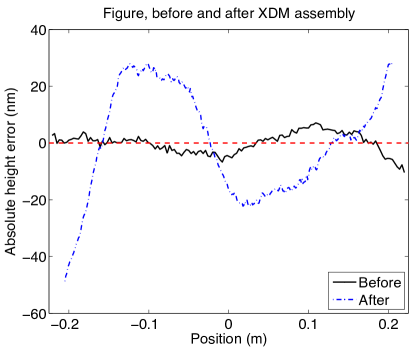
The substrate’s figure was measured with the interferometer described above, both before and after actuator bonding and mirror assembly. Figure 4 presents both measurements.
After polishing and before assembly the figure error was 3.5 nm rms. After assembly at uniform voltage the figure error was 19 nm rms. This amount is well within the dynamic range of the mirror to self-correct (as it was designed to be). To remove this 19 nm rms figure error, we must determine the proper voltages.
V Characterization and control of the deformable mirror
Just as in astronomical or vision-science adaptive optics, the challenge of controlling the XDM is to determine the set of commands that produce a desired shape on its surface. In our experimental setup we have a very high-quality height measurement of the surface. Given this height, we must “fit” it to the deformable mirror by determining the set of actuator commands that best corrects that shape. (See Ellerbreok MVU for a thorough discussion of this concept in the field of astronomical adaptive optics).
If our XDM is a linear system (which it approximately is), we can describe it with a simple matrix equation. Given a vector of 45 voltages , the height made on the surface of the XDM follows the matrix equation
| (1) |
where the matrix describes the response of the XDM. In this case the height has the same sampling and number of pixels as the stitched interferometer measurements. Then, given a desired height shape on the XDM, we can “fit” the height and estimate the voltages by solving the inverse problem. In the following subsections we discuss how to obtain , if the underlying assumptions of the linear model are true, and how best to go about solving the inverse problem given the unique characteristics of the XDM.
As noted above the mirror is commanded around a non-zero bias voltage which produces a surface with no cylinder. So for clarity in notation, for the remaining treatment assume that the vector represents the voltage value relative to bias, as opposed to the actual voltage commanded through the electronics.
V.1 Influence function
The term influence function refers to the shape that the XDM makes in response to voltage applied to a single actuator. During the development and design of the XDM, a detailed finite-element-analysis model was constructed. It produced the estimated influence function for each of the 45 actuators on the XDM, sampled at 1 mm per pixel. By taking the output of the FEA model along the centerline of the XDM, we can populate the matrix , with each column representing the height made by one actuator. The XDM cannot make tilt across its full length, and the influence functions contain no tilt. They are furthermore offset to have no piston (average value), which cannot be measured by the interferometer and is irrelevant to the wavefront error.
Just such a matrix was used for our initial control of the XDM. To determine how accurate the model was, we performed an actuation test. The mirror was commanded to bias voltage, and then one actuator was commanded to 30 V above bias, or half the total voltage range. This pair of moves was repeated for all 45 actuators. This entire process was done in each of the mirror’s three mount positions. To analyze the data, the measurement at bias was subtracted from the measurement when an actuator was commanded to produce a change in surface figure. (This is necessary to remove the figure of the XDM at bias voltage, which the FEA model does not know about.) Finally, for each actuator the measurements at the three mount positions were stitched together. The response of actuator 25 is shown at top in Figure 5.
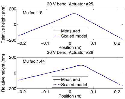
As with all actuators, the shape agrees very well with the model but the magnitude is higher than the FEA predictions. The parallel actuator configuration utilizes the in-plane strain of the PMN for actuation therefore the stroke of the PMN actuators can not be directly measured before assembly. To guarantee that the stroke requirements are met, the XDM was designed with a conservative actuator strain learned from heritage AOX mirrors. A scaling factor of 1.8 was used to match the magnitude of the conservative FEA result with the actual measured stroke.
This analysis was done for all 45 actuators. Each actuator has a unique influence function - actuators closer to the edge have less displacement. Most actuators had this same 1.8 scaling factor but four did not. Actuator 28 is shown at bottom in Figure 5. For this actuator the shape agreement is excellent, but now the scaling factor is 1.44. This means actuator 28 does not respond as much to the same voltage as most other actuators.
After this full characterization, we modified the initial that was based on the FEA model. Most columns were multiplied by 1.8 to reflect the actual behavior of the XDM. Actuators 27, 28, 36 and 37 were given different scaling factors based on the analysis described as above. This produced our final matrix.
Given this model, we can evaluate the dynamic range of the XDM as built. By commanding all actuators uniformly to either maximum or minimum voltage, we can make 7.4 microns peak-to-valley cylinder in either direction. Due to the broadness of the influence function, stroke goes down rapidly with spatial frequency. The model indicates that the XDM can make 750 nm peak-to-valley of a sine wave of two cycles across the 45 cm length, but only 40 nm peak-to-valley of a sine wave of eight cycles. This is more than sufficient to self-correct the mirror, as we demonstrate below.
V.2 Verification of linearity
The fundamental assumption behind Equation 1 is that the XDM behaves as a linear system. This requires two thingsOpWil . First, given two different inputs and that produce outputs and , the sum of the inputs must produce an output that is equal to the sum of the individual outputs . This property of linear superposition holds true for piezo-actuated DMs made previously by Xinetics.
We did several experiments to verify that this was the case in the XDM as built. As shown in Figure 6, superposition holds very well.
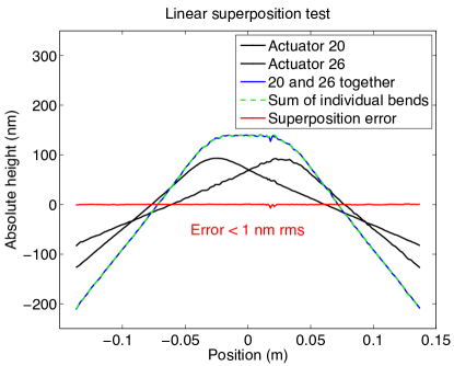
In this case we commanded first actuator 20, then actuator 26 above bias individually. Then we commanded them at the same time. We evaluated the change in height by subtracting from each a measurement at bias voltage. The actual measurement of actuators 20 and 26 commanded together is very nearly the same as the sum of the two individual measurements.
The second aspect of linearity is that if we scale the input by a constant, then the output is scaled by the same constant. The response of the XDM to voltage is close enough to linear that this assumption is valid. Since hysteresis only about 1%, we can treat the XDM as a linear system and use the matrix equation to control it. The validity ignoring hysteresis and assuming perfect linearity will be studied in future work.
V.3 Fitting the height with a matrix or non-linear optimization
Now that we have determined that the matrix describes our actual XDM, we can use such a matrix approach. The final question is how do we actually implement the solution to the inverse problem. In adaptive optics, the standard approach Hardy is to calculate the pseudoinverse of and estimate the voltages with
| (2) |
The pseudoinverse is usually calculated with a singular value decomposition (SVD). However, care must be taken in the pseudoinverse process to reject very small singular values (for example, see the discussion in Gavel GavelWaffle on this problem and possible better approaches).
Characteristics of the XDM make the SVD approach workable, but only with caution. In particular the broadness of the influence function means that there is a huge dynamic range variation with spatial frequency. While the XDM can make several microns of cylinder, it can make only a few nanometers of the highest spatial frequencies. When calculating the SVD, the singular values for span a range of over 100,000. If all singular values are included when the pseudoinverse is calculated, huge noise inflation can occur. However, if too many singular values are suppressed, very little of the height shape will be correctly fitted. Through an analysis of different levels, we have determined that the best tolerance results in keeping the 21 largest singular values and those modes in the SVD. As a result we correct only about half of the full frequency range possible on the XDM, up to a spatial period of 4 cm.
In practice the SVD works well, but due to rejecting just over half of the modes, we wanted to explore other options. At the present computational costs are not a significant factor, so we explored optimization methods. These have been used elsewhere in AO Pueyo2009Optimal-dark-ho to control DMs. We implemented a variety of optimization methods with functions in Matlab’s Optimization Toolbox. Simulations with model influence functions were used to study several options, including Matlab’s linear programming method to minimize either the L1 norm, the L-infinity norm or to minimize the actuator stroke. We also used Matlab’s quadratic programming method to minimize the L2 norm. Of these options, the quadratic programming method worked the best. In simulations it produced the least figure error and did not have issues with convergence. We implement the L2-norm optimization with an initial estimate of the voltages obtained with use of the psuedoinverse matrix, and then use the option - and constraint the actuator voltages to change by no more than 10% of the total range. Both of these methods work well and give us a way to convert of precision metrology to actuator commands.
VI Flattening of the deformable mirror
The tools described above allow us to calculate voltages that reduce the controllable figure error on the XDM surface. Our requirement is to flatten the XDM to the same level of controllable error as before assembly (3.5 nm). Our goal is to flatten it to better than 1 nm rms.
One approach to flattening the XDM is to take a single stitched measurement of its full figure, determine new voltages from that measurement, and apply them. In practice, this approach does not achieve our goal. This is due to either errors in the model, or non-linear effects such as hysteresis. Such an “open loop” approach will be explored in future work. The second approach is to try a “closed loop” control where we take a series of measurements, each time feeding back the residual error and integrating it. This approach overcomes hysteresis and some non-linear effects, and we have found it to be reliable and stable.
VI.1 Flattening one position
For correcting a sub-section of the XDM (e.g. in center position only), this whole operation proceeds rapidly. The XDM is initially placed at bias voltage. Given a calibrated measurement, piston and tilt are removed. This residual is sent to an integral controller with gain 0.5 and memory 0.999. Because the interferometer view is smaller than the XDM’s length, we extrapolate the signal beyond the viewing area to the full 45 cm, in the process minimizing XDM curvature. This modified height vector is then used for the inverse problem to estimate voltages, which are applied to the XDM. A new calibrated measurement is taken and the process repeats. This converges to better than 1 nm figure error in five steps or fewer. We can typically achieve between 0.5 and 0.6 nm rms controllable figure over a 20 cm length section of the XDM, with an occasional best correction down to 0.45 nm or below.
VI.2 Flattening the entire length
Flattening the entire length is more of an experimental challenge. Changing position requires physically moving the XDM about 8 cm, adjusting the fringes on the interferometer, and waiting for the air in the enclosure to settle. More problematic is that every time the XDM is moved, there is the potential for changing its figure. The connection cables off the back are numerous and quite thick, and moving them can change the surface figure (as is easily seen in a real-time change of the fringes on the interferometer display). The cables are draped on a smooth stand to reduce forces on them when the mount is translated.
Once the repeatability challenges with moving the XDM have been overcome, we still have a question of time efficiency. We could do the same closed-loop approach as above for one position, except taking three measurements each time. This method would be very labor and time intensive. Instead we flatten the XDM as above for the center position, and then move to the right position. In right position, the portion of the XDM that was corrected in center is still extremely flat, while the portion near the mirror’s edge that was out of the center field of view is uncorrected. To correct only this new portion, and ensure that we do not introduce error where the views overlap, we align the residual measurement so that the previously-corrected portion has no tilt. To combine this with the previous shape on the XDM, we take the previous voltages and estimate the correction through multiplication with the matrix. We then add the residual to this; since the previously corrected portion has no tilt, this adds nothing to the unmeasured portion of the XDM. Only the new portion seen in right position has a non-zero residual. We then solve the inverse problem (as described above) to obtain the new voltages.
This process in essence changes the voltages so that the previously uncorrected part of the right view is corrected, while preserving the flat surface shape in the center section. In practice we usually use the quadratic programming optimization and the result is under 1 nm rms figure error in less than five iterations. Once the right position is flattened, we move to left and correct that remaining portion in a similar manner.
At the end of this process we have a complete voltage set, which we place on the XDM and measure at each of the three positions. The figure error is typically under 2 nm. We then use this stitched calibrated measurement to update the voltages. We estimate the correction shape made by the entire mirror by taking the voltages and multiplying by the matrix. We then add the stitched residual, and solve the inverse problem to fit this new height. Typically one or just two iteration of this is all that is necessary to produce a controllable figure error of less than 1 nm rms.
To demonstrate this process we have executed it three times, producing controllable figure errors of under 1 nm rms. The three results are shown in Figure 7.
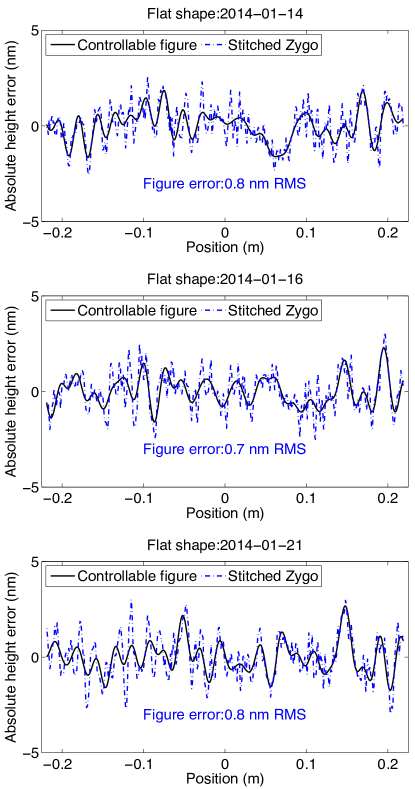
All runs occurred in January 2014. On the 14th, we achieved 0.8 nm rms controllable figure error. On the 16th, we achieved 0.7 nm rms controllable figure error. On the 21st, we achieved 0.8 nm rms controllable figure error. These are calculated across a 43.8 cm length on the XDM. As discussed below, these three trials represent different realizations of the same fundamental flattening process in the presence of noise.
Sub-sections of these measurements are even flatter. In the January 16th measurement a 21.6 cm section from x positions -8 cm to 13.6 cm has 0.5 nm rms controllable figure error. This number is also readily achievable in flattening a 20-cm section of a single view of the XDM, as described in the previous section.
The three residual figure errors shown in Figure 7 all look different, indicating that we have no static error source that is limiting correction. We can further analyse the results by estimating the spatial power spectral densities (PSDs) through the modified periodogram method DSP (i.e. with a Hanning window in Matlab). As shown in Figure 8, the three trials all have similar power through the controllable region.
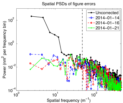
We are not significantly correcting modes with periods shorter than 4 cm, which is consistent with the limitations of the inversion methods and the single-position flattening results mentioned above.
Each of the three experiments was conducted from an initial condition of bias voltage for all actuators. The difference final voltages applied to the XDM from the average voltages for the three trials are shown in the top of Figure 9.
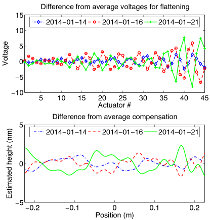
Though the low numbered actuators all track extremely well, there is difference in the middle and especially high numbers. However, these differing voltage sets produce nearly the same shape, as shown with the difference from average compensation at bottom in the Figure. The estimated compensation was calculated with the matrix. Different voltages producing nearly the same figure is possible for two reasons. First, the voltages represent curvature, not position. Second, the actuators near the edge bend the XDM very little and translate into small figure changes. The shape made the XDM is estimated to vary by only a few nanometers across the entire length. This points to the stability of the overall figure error on the XDM and robustness of our algorithms and experimental procedures.
At this time our largest error sources are intrinsic to the experimental setup. These are the small changes in figure as the temperature changes with time during the trials, and any small distortions of the XDM surface as the mount is moved and forces on the cables change. Even with these errors, we can still reliably and repeatably achieve sub-nanometer flattening of the entire XDM length from zero initial conditions.
These surface figure measurements are done with visible light metrology and are not directly comparable to an at-wavelength focusing test, such as that conducted by Mimura et al. Mimura2010Breaking-the-10 . Final focus spot size will depend not only on the figure of the XDM, but on the x-ray wavelength, F-number of the final focusing optic, the incident graze angle, as well as the net sum rms figure error of all the optics
Rayleigh’s criterion implies near diffraction limited focus is possible when the optical path difference over the aperture is (rms figure error/16)/grazing incidence angle. At 10 keV energy, this corresponds to an rms figure error 0.008 nm/graze angle. Assuming the mirror used at 1 milli-radian graze angle (typical for mirrors this long), this corresponds to surface normal figure error of 8 nm rms. Hence, the sensitivity of our surface normal mirror correction is more than adequate to meet this requirement.
In summary, we have flattened our XDM to a flatter figure than the best previously published results (detailed above in Section I) for a deformable mirror of similar length (35 cm). Our sub-nm flattening level is comparable to the best achieved by other deformable optics, but on a substrate more than three times as long (45 cm vs 12 cm).
VII Conclusions and Future Work
We have manufactured a 45-cm long x-ray deformable mirror. The initial substrate was polished to 3.5 nm rms figure error; after actuator bonding and mirror assembly this error became 19 nm rms. We have used very precise visible-light interferometry and detailed characterization of the XDM to perform closed-loop control to flatten its surface. Starting from zero initial conditions, we can reliably and repeatedly flatten the controllable figure of the XDM to sub-nanometer levels. Our best correction of the full length is 0.7 nm RMS; for smaller 20-cm sections was have achieved 0.5 nm rms.
The next challenge is to maintain such a flat shape through time without the use of external metrology. Our XDM has 45 strain gauges (one per actuator) and eight temperature sensors. These will be used to correct for both temperature dependent changes in figure as well as other non-linear effects, such as time-dependent changes in the PMN response. In our future work we will conduct a full characterization of the gauges and sensors. Once calibrated, we will use them for feedback control to maintain both the cylinder and figure of the XDM over periods of several hours. A secondary task is to better understand the single-step shaping of the XDM, and whether we are limited by knowledge of the influence functions, hysteresis, or some other factor. Once we can reliably flatten and maintain the XDM as flat, and make arbitrary shapes, we will move on to at-wavelength testing of the XDM at the Advanced Light Source at Lawrence Berkeley National Laboratory. Of particular interest are studying different wavefront sensing methods to provide accurate and rapid in situ metrology of the XDM.
Acknowledgments
This work performed under the auspices of the U.S. Department of Energy by Lawrence Livermore National Laboratory under Contract DE-AC52-07NA27344. The document number is LLNL-JRNL-649073. Early technology development was supported at NG-AOX through internal research and development funding. The authors thank Brian Bauman (optics), Carol Meyers (optimization methods), and Peter Thelin (laboratory facilities) for their advice or assistance. The authors also thank the reviewers for their diligent evaluation and helpful comments that have improved this paper.
References
- (1) H. Mimura, S. Handa, T. Kimura, H. Yumoto, D. Yamakawa, H. Yokoyama, S. Matsuyama, K. Inagaki, K. Yamamura, Y. Sano, K. Tamasaku, Y. Nishino, M. Yabashi, T. Ishikawa, and K. Yamauchi, “Breaking the 10 nm barrier in hard-x-ray focusing,” Nature Physics 6, 122–125 (2010).
- (2) T. J. McCarville, P. M. Stefan, B. Woods, R. M. Bionta, R. Soufli, and M. J. Pivovaroff, “Opto-mechanical design considerations for the linac coherent light source x-ray mirror system,” (2008), Proc. SPIE 7707, pp. 70770E–70770E–11.
- (3) A. Barty, R. Soufli, T. McCarville, S. L. Baker, M. J. Pivovaroff, P. Stefan, and R. Bionta, “Predicting the coherent x-ray wavefront focal properties at the linac coherent light source (lcls) x-ray free electron laser, ”Opt. Express 17, 15508–15519 (2009).
- (4) JTEC Corporation, X-ray focusing mirror, http://www.j-tec.co.jp/english/focusing/index.html”
- (5) P. Mercere, M. Idir, G. Dovillaire, X. Levecq, S. Bucourt, L. Escolano, and P. Sauvageot, “Hartmann wavefront sensor and adaptive x-ray optics developments for synchrotron applications,” in “Adaptive X-Ray Optics,” , A. M. Khounsary, S. L. O’Dell, and S. R. Restaino, eds. (2010), Proc. SPIE 7803, p. 780302.
- (6) K. J. S. Sawhney, S. G. Alcock, and R. Signorato, “A novel adaptive bimorph focusing mirror and wavefront corrector with sub-nanometre dynamical figure control,” in “Adaptive X-Ray Optics,” , A. M. Khounsary, S. L. O’Dell, and S. R. Restaino, eds. (2010), Proc. SPIE 7803, p. 780303.
- (7) H. Mimura, T. Kimura, H. Yokoyama, H. Yumoto, S. Matsuyama, K. Tamasaku, Y. Koumura, M. Yabashi, T. Ishikawa, and K. Yamauchi, “An adaptive optical system for sub-10nm hard x-ray focusing,” in “Adaptive X-Ray Optics,” , A. M. Khounsary, S. L. O’Dell, and S. R. Restaino, eds. (2010), Proc. SPIE 7803, p. 780304.
- (8) T. Kimura, S. Handa, H. Mimura, H. Yumoto, D. Yamakawa, S. Matsuyama, Y. Sano, K. Tamasaku, Y. Nishino, M. Yabashi, T. Ishikawa, and K. Yamauchi, “Development of adaptive mirror for wavefront correction of hard x-ray nanobeam,” in “Advances in X-Ray/EUV Optics and Components III,” , S. Goto, A. M. Khounsary, and C. Morawe, eds. (2008), Proc. SPIE 7077, p. 707709.
- (9) C. Svetina, D. Cocco, A. Di Cicco, C. Fava, S. Gerusina, R. Gobessi, N. Mahne, C. Masciovecchio, E. Principi, L. Raimondi, L. Rumiz, R. Sergo, G. Sostero, D. Spiga, and M. Zangrando, “An active optics system for euv/soft x-ray beam shaping,” in “Adaptive X-Ray Optics II,” (2012), Proc. SPIE 8503, pp. 850302–850302–8.
- (10) N. A. Artemiev, D. J. Merthe, D. Cocco, N. Kelez, T. J. McCarville, M. J. Pivovaroff, D. W. Rich, J. L. Turner, W. R. McKinney, and V. V. Yashchuk, “Cross comparison of surface slope and height optical metrology with a super-polished plane si mirror,” (2012), Proc. SPIE 8501, pp. 850105–850105–11.
- (11) S. Rutishauser, L. Samoylova, J. Krzywinski, O. Bunk, J. Grunert, H. Sinn, M. Cammarata, D. M. Fritz, and C. David, “Exploring the wavefront of hard x-ray free-electron laser radiation,” Nat Commun 3 (2012).
- (12) G. E. Sommargren, D. W. Phillion, M. A. Johnson, N. Q. Nguyen, A. Barty, F. J. Snell, D. R. Dillon, and L. S. Bradsher, “100-picometer interferometry for EUVL,” (2002), Proc. SPIE 4688, pp. 316–328.
- (13) D. Malacara, Optical Shop Testing (John Wiley and Sons, 1992).
- (14) E. L. Church, “Fractal surface finish,” Appl. Opt. 27, 1518–1526 (1988).
- (15) B. L. Ellerbroek, “Efficient computation of minimum-variance wave-front reconstructors with sparse matrix techniques,” J. Opt. Soc. Am. A 19, 1803–1816 (2002).
- (16) A. V. Oppenheim, A. S. Willsky, and S. H. Nawab, Signals and Systems (2nd Ed.) (Prentice Hall, New Jersey, 1997).
- (17) J. W. Hardy, Adaptive Optics for Astronomical Telescopes (Oxford University Press, New York, 1999).
- (18) D. T. Gavel, “Suppressing anomalous localized waffle behavior in least squares wavefront reconstruction,” (2002), Proc. SPIE 4839, pp. 972–980.
- (19) L. Pueyo, J. Kay, N. J. Kasdin, T. Groff, M. McElwain, A. Give’on, and R. Belikov, “Optimal dark hole generation via two deformable mirrors with stroke minimization,” Appl. Opt. 48, 6296–6312 (2009).
- (20) A. V. Oppenheim, R. W. Schafer, and J. R. Buck, Discrete-time Signal Processing (Prentice Hall, New Jersey, 1999).