Negative Differential Resistance due to Nonlinearities in Single and Stacked Josephson Junctions
Abstract
Josephson junction systems with a negative differential resistance play an essential role for applications.
As a well known example, long Josephson junctions of the BSCCO type have been considered as a source of THz radiation in recent experiments.
Numerical results for the dynamics of the fluxon system have demonstrated that a cavity induced negative differential resistance plays a crucial role for the emission of electromagnetic radiation.
We consider the case of a negative differential resistance region in the McCumber curve itself of a single junction and found that it has an effect on the emission of electromagnetic radiation.
Two different shapes of negative differential resistance region are considered and we found it is essential to distinguish between current bias and voltage bias.
Keywords: Millimeter wave devices, superconducting devices, nonlinear circuits, nonlinear optics, nonlinear oscillators
I Introduction
Fluxon dynamics in long Josephson junctions is a topic of strong interest due to its rich nonlinear properties and applications in fast electronics, in particular as a radiation source at high frequencies Ozyuzer07 ; Wang10 ; Koshelets00 ; Kashiwagi12 . An extension of that system is to form a metamaterial by stacking several Josephson junctions on top of each other, which are modeled by coupled partial differential equations.
Such superconductors are employed in a variety of devices (stacks, flux-flow devices, and synchronized arrays) and are capable of power emission in the range 0.5-1 THz. Integration in arrays could give an improvement in the power performances, above Welp13 . Practical applications are especially in the field of bio-sensing, nondestructive testing and high speed wireless communications Welp13 . For such reasons we aim to understand if some simple mechanism is at work in all these devices. Such a system is used as a model for high temperature superconductors of the BSCCO type Tachiki09 ; Welp13 . In this communication we go one step further in complexity and include results on a nonlinear behavior of the shunt resistor, giving rise to features similar to stacked Josephson junctions coupled to a cavity Madsen08 ; Madsen10 ; Tachiki11 ; Tsujimoto10 . Such a model is needed in order to understand and interpret the experimental measurements. For frequencies in the GHz or even THz range, either an intrinsic or an external cavity is needed to enhance the radiated power to useful levels. Figure 1a shows qualitatively the appearance of a nonlinear current-voltage (IV) curve for the quasi particle tunneling in the Josephson junction. The particular form of the IV curve resembles a distorted N and hence we refer to this particular form as -shaped IV curve. Note that the quasi particle tunnel current is a unique function of the applied voltage, but the inverse function is not unique. Similarly, Fig. 1b depicts an IV curve, which is shaped as a distorted (-shaped IV curve). In this latter case the voltage is a unique function of the current. In general the nonlinear behavior leading to a negative differential resistance (NDR) of Josephson junctions plays a key role for applications. An example is a parametric amplifier or a radiation source at high frequencies Soerensen79 ; Wahlsten77 ; Pedersen73 . Examples of NDR are numerous: (i) Josephson junction with a cavity Barbara99 ; Filatrella03 , (ii) backbending of the BSCCO energy gap Welp13 , (iii) structure at the energy gap difference if the junction consists of two different superconductors, (iv) in connection with Fiske steps, zero field steps Cirillo98 and even in rf-induced steps Pedersen80 . In some cases of NDR a nonlinear region that cannot be explained shows up in the IV curve Kadowaki . The two qualitatively different cases of a nonlinear differential resistance, referred to as -shaped and -shaped regions, observed in experiments will be discussed in the next sections. We mention that besides the NDR at finite voltages, also absolute negative resistance Nagel08 and negative input resistance at zero voltages Pedersen76 have been reported.
In this work we want to emphasize the role of nonlinearities and to show that even a very simple model can give rise to an interesting power emission profile. However, our model, being a high frequency model, cannot capture effects at low timescale, such as thermal effects Wang10 ; Yurgens11 ; Li12 ; Gross13 . We discuss below various examples of a negative differential resistance in Josephson junctions.
II Negative differential resistance at finite voltages
Josephson junctions come in a variety of forms with different properties but the same generic behavior. Some examples are: (i) The traditional low temperature () Josephson junction with qualitatively different behaviors depending on the dimensions of the junction, (ii) high intrinsic Josephson junctions that are typically described as a stack of long Josephson junctions leading to coupled sine-Gordon equations and (iii) point contacts and microbridges that are the easiest to describe mathematically. Some features are generic, like the Josephson voltage to frequency relation, the supercurrent, the energy gap etc. In all cases we may have a coupling to a cavity either intrinsic (internal) or external, which of course complicates the mathematics but may be important for applications.
The two different cases of negative differential resistance – -shaped and -shaped – discussed here are shown in Fig. 1.


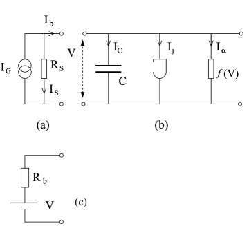
Fig. 1a shows schematically both the NDR IV curve of a semiconductor Gunn diode wikipedia1 (which is used as a microwave source) as well as that of a Josephson junction coupled to a cavity Madsen10 . This type of IV curve is sometimes referred to as an -shaped IV curve wikipedia1 .
The analogy with Gunn diode is purely hypothetical. We speculate that the NDR IV characteristic, even if of very different nature, could be similar to Josephson junction NDR at a phenomenological level. This is only an observation, and we do not claim that the constitutive physics is the same. In order to measure the NDR part of the IV curve in Fig. 1a, we must have a constant voltage bias source. With a constant current bias source we will see hysteresis when increasing and decreasing bias current (dashed line) . For the Josephson junction the cavity may typically look as the hysteretic curve if the junction is current biased or as the continuous curve (full line) when voltage bias. In most cases the experimental curves for Josephson junctions are current biased although voltage bias can also occur Gokhfeld07 .
Figure 1b shows another type of NDR curve referred to as -shaped. Here a constant current bias source is needed to trace out the full curve. In reference Ozyuzer07 a NDR region qualitatively similar to that in Fig. 1b is observed together with radiation emission. Since additionally in Ozyuzer07 radiation emission is also observed in a part of the IV curve that looks qualitatively similar to that in Fig. 1a, it is tempting to link the radiation emission with the NDR. We note that a Josephson junction is nonlinear up to very high frequencies (THz), implying that it’s negative resistance may have important high frequency applications: examples are (i) a high frequency parametric amplifier and (ii) a generator for high frequency electromagnetic radiation. We note from Fig. 1 that we have 4 different combinations of the bias and nonlinearity. In the general case the bias is neither current nor voltage biased but has a load line that is neither vertical nor horizontal. However, a pure voltage bias is not conceivable for a superconducting element, and therefore there is not a full symmetry between the two cases, as can be seen in the following.
For intrinsic Josephson junctions the NDR qualitatively shown in Fig. 1b comes from the well known back bending of the IV curve near the energy gap due to heating. There are other shapes than -shaped and -shaped, an example from semiconductors is the -shape
A diagram showing the model we are discussing is depicted in Fig. 2. Here the left part of the figure shows the two different bias circuits, the middle part (b) shows the Josephson junction model with the nonlinear resistor and the capacitor.
We do not hypothesize on the physical origin responsible for the NDR. Instead, a phenomenological IV characteristic of the effective shunt encompasses the behavior of the interaction with an external load. Shortly, we adopt the following logic: the observed IV of loaded stacks exhibits a NDR, therefore we introduce a nonlinear effective shunt resistor.
For the bias circuit we distinguish between (a) current bias and (c) voltage bias. In the case of current bias the shunt resistance is large and for the voltage bias case the bias resistor is small. We underline that leads to an unphysical result for a superconducting element as the Josephson junction. In fact a dc voltage produces an ac current through the Josephson junction element, while the capacitor remains inactive and the resistor current is constant.
The actual bias at high frequency is more complicated than elements (a) and (c) of Fig. 2 Likharev86 , and we use such very simple schemes for sake of simplicity. We notice that in experiments a partial voltage bias has been employed (e.g., Ozyuzer07 ; Welp13 ), and a voltage bias is sometimes used in modeling (e.g.,Gokhfeld07 ); the interface between the voltage source and the mesa at THz frequencies leads to a very difficult full wave electromagnetic problem.
In the following we shall set up a mathematical model for the Josephson junction circuits depicted in Fig. 2. The voltage across the Josephson junction is denoted = and it depends on time . The Cooper pair phase difference across the Josephson barrier is = and the Josephson voltage relation reads =. The electron charge is and denotes Planck’s constant divided by . . We model the -type NDR characterized by a nonlinear conductance shaped as a Gaussian function
| (1) |
Here is the linear quasi particle conductance (related to the quasi particle resistance ) and describes the nonlinear part of the conductance.
The parameter position the Gaussian function along the -axis and is a measure of the Gaussian width.
The Gaussian model is phenomenological – it is only a way to create the negative differential resistance. In fact, we have also tried with other functional shapes (e.g. polynomial), obtaining the same qualitative result: an increase of the power associated with the NDR branch, as in Ozyuzer07 ; Welp13 . A detailed comparison that could give a quantitative evaluation of the parameters and is out of the scope of this paper, which aims to a phenomenological description.
The quasi particle tunnel current is then given by
| (2) |
In Fig. 2 denotes the bias current supplied by the current source in the circuit (a) or voltage source in the circuit (d), is the displacement current through the capacitor and the Josephson tunnel current is denoted = , where is the Josephson critical current. The current balance becomes . Inserting the Josephson voltage relation and Eq. (2) into the current balance equation gives
| (3) |
The above Eq. (3) can be transformed into normalized units using the scaling , with , thereby we obtain
| (4) |
Here the nonlinear conductance has been normalized and leads to the nonlinear dissipation term with in
| (5) |
In the above expression , , and is the normalized voltage. The equations reduce to the usual RSJ model for .
| (6) | |||||
| (7) |
where is the tridiagonal matrix that describes the coupling among the superconducting layers Sakai93 . The matrix reads in the diagonal, and the coupling constant otherwise. In the following we will adopt the phenomenological model (4) that qualitatively describes the NDR obtained by the full model (6,7) (see Ref. Madsen10 ).
III -shaped resistor
Inserting a -shaped resistor in , see Eq.(5), leads to current voltage curves of the form depicted in Fig. 4. The model for the -shaped resistor can also be used in the case of voltage bias, where the normalized current reads (see Fig. 2):
| (8) |
where is the normalized resistance of Fig. 2c. The expression in (8) can be inserted into the system equation (4), which reduces to the current bias when and . In this setup we consider open circuit boundary conditions. More realistic boundary conditions as an RLC circuit will be discussed elsewhere unpublished_C .
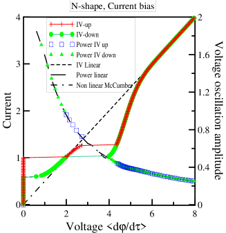
In Fig. 4 the available power is estimated through the oscillations of the Josephson voltage. We underline that in this paper we refer to available power, or shortly power (also in the figure labels), as the maximum power that could be extracted supposing a perfect matching with the external device. The optimization of this important effect is relevant for the application, but in this paper we focus on the existence of a general effect due to NDR. The power estimate is done recording the JJ waveforms and extracting the difference between the maximum and the minimum, that it is proportional to the mean square amplitude in the sinusoidal regime. The features of the power estimate are generic and consistent with a full Fourier analysis of the waveform. The nonsinusoidal response of a single JJ at low bias is enhanced and results in a high harmonic content at low bias, close to the return point on the IV. The voltage oscillations seems to go towards infinity at low dc voltage. As it is well known Likharev86 , the actual power is peaked at some (low) frequency and goes towards zero at high frequencies (due to capacitance ) and low frequencies (due to inductance). It is also known that there is a phase change in the ac-voltage (respect to the ac current) as we decrease bias current, such that will not increase.
Moreover, in our calculations we only find the rising branch that is stable, and that abruptly switches to zero voltage at a finite level of amplitude (corresponding to a finite current before the switch to the Josephson supercurrent). Applicationwise the most interesting region is above the peak when the voltage, and hence the frequency of the emitted radiation, span the THz region.
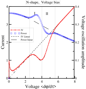
In summary, from Figs. 4, 4 it is evident that: (i) The nonlinear McCumber branch causes a hysteretic behavior. (ii) The output power, i.e. the amplitude of the Josephson voltage oscillations, is nonlinear in the region of McCumber nonlinearity. (iii) The negative branch of the nonlinearity (region I in Fig. 4, corresponds to a power higher than the power obtained from a linear McCumber resistor. This is only evident in the case of voltage bias, for the nonlinear part is unstable with a current bias. (iv) The reverse is true for the positive branch of the nonlinearity (region II in Fig. 4), where the available power is lower than the power obtained from a linear McCumber resistor.
IV -shaped resistor
An -type NDR may also be found in a Josephson junction. The most obvious example is the back bending of the IV curve in an intrinsic Josephson junction at the energy gap Welp13 . This case is mathematically more complex than the -type. For the -type case we noticed that to have a continuous IV curve with NDR we should have voltage bias (Fig. 1a). Most experiments on Josephson junctions are current biased and give rise to hysteresis (See Fig. 4). For -type nonlinearity the situation is the inverse. The continuous IV curve is obtained with current bias whereas with voltage bias switching will result (Fig 1b).
If we consider a current biased Josephson junction circuit with an -type nonlinearity (see Fig. 1b) we obtain for a nonlinear resistor:
| (9) | |||||
| (10) |
That reduces to the linear case for . As usual with the current balance one gets the set of equations:
| (11) |
Inserting the expressions for the current through the capacitor () and the Josephson element () one retrieves the second order set of differential equations:
| (12) |
That can be cast in normalized units (with the standard definitions of Josephson angular velocity and dissipation ) in a system of two equations:
| (13) |
Here the nonlinear conductance has been normalized and gives rise to nonlinear dissipation :
| (14) |
where . The equations can be finally cast in normal form with the variables and :
| (15) |
The equations reduce to the usual RSJ model for :
The dissipation is employed to write the system of differential equations for the variables and that is true for any functional dependence of the nonlinear dissipation upon the resistor current
| (16) |
In general, for any -shaped conductivity we can define as the ratio between the bias and the dissipation
| (17) |
The system of Equations (IV) can be written:
| (18) |
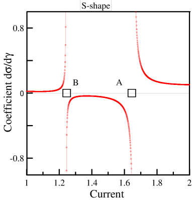
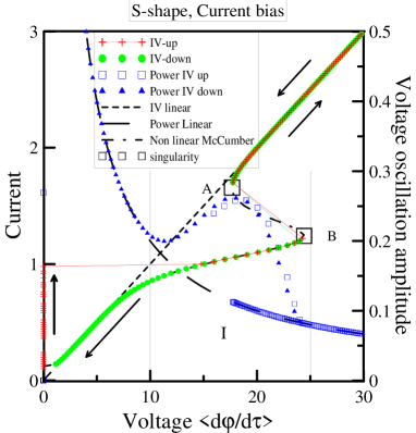
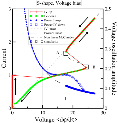
The coefficient of the right hand side is the nonlinear differential conductance. Unfortunately for an -shaped IV curve this is a term that vanishes in two points, see Fig. 5. For the model (17), of the analytical expression of (see Eq.(17)), reads:
| (19) |
The system becomes singular (non Lipschitzian) for two values of the current, where the differential conductance vanishes. Also, for negative values the system cannot be integrated
| (20) |
Therefore, for the -shaped case, one branch of the IV (and the corresponding power) cannot be reproduced, see Fig. 7. A linear perturbation analysis of Eq.(IV) around the singular points (20), can be accomplished setting :
| (21) |
Eqs. (IV) predict that for small (in the proximity of the singular point) the differential equations are not well defined. In the figures for the -shaped resistor in fact squares denote the point implicitly defined by such condition, that well agree with the point where the differential equation cannot be numerically integrated. Inserting an -shaped resistor in one gets in the simulations a typical result in Fig. 7. Also for the -shaped resistor we can assume a voltage bias, see Fig. 7. The normalized current is the same as in Eq. (8), that inserted into the system equation reads:
| (22) |
The system reduces to the current bias when and .
V Figure discussion
We note that there are no stable bias points between and in Figs. 7 and 7. Increasing the bias current from zero in Fig. 7 we first have a supercurrent until the current is where we have a switching to the lower branch of the IV curve. Increasing the bias current further we reach point . Still increasing the bias current from we continue from point . We note that the power () dissipated in and are the same so the transition between and is rather unusual. There are no stable bias points between and and it is not a usual switching along a vertical or horizontal line.
Figures 7,7 include Josephson radiation in terms of voltage amplitude. In both Figs. 7 and 7 we also have unusual radiation patterns. Decreasing the bias current from above in Fig. 7 we see the following: we observe radiation corresponding to the standard McCumber curve, until we reach . From here we continue down from and the radiation follows a new curve showing a peak deviating from the standard McCumber curve in region . Increasing the bias current from zero we have the switching at , but otherwise the radiation is the same as we had for decreasing bias current. Thus even if we have two branches of the radiation curves we do not have hysteresis in the usual sense. Figure 7 with constant voltage bias shows essentially the same features.
VI Summary
-type and -type nonlinearities have been investigated in the McCumber curve for point Josephson junctions.
A fictitious NDR, Gaussian shaped, perturbation of the standard McCumber dissipation is introduced to take into account the complicated electrodynamic interaction between stacks of JJ and the load. This allows us to obtian -type and -type nonlinearities that posses differential resistance. We found that the current-voltage characteristics of the full RSJ Josephson junction model is very much influenced by a nonlinearly shaped McCumber curve leading to hysteresis and enhanced emitted radiation power in the region with negative differential resistance. Current-voltage curves were obtained for both current bias and voltage bias. More realistic high frequency schemes of the voltage bias and of the lumped elements could be attempted in further investigations. Our model governs a simple point Josephson junction, but the results can be applied to phase locked stacks of Josephson junctions, e.g. coupled via a common RLC cavity circuit.
Acknowledgements
We thank COST program MP1201 Nanoscale Superconductivity: Novel Functionalities through Optimized Confinement of Condensate and Fields (NanoSC -COST) for partial support. GF work at the DTU was supported by the COST “Short Term Scientific Mission” COST-STSM-ECOST-STSM-MP1201-291013-036429. VP thanks INFN (Italy) for partial support.
References
- (1) L. Ozyuzer, A.E.Koshelev, C.Kurter, N. Gopalsami, Q. Li, M. Tachiki, K. Kadowaki, T. Yamamoto, H. Minami, H. Yamaguchi, T. Tachiki, K. E. Gray, W.-K. Kwok, and U. Welp, “Emission of Coherent THz Radiation from Superconductors,” Science, vol. 318, no. 5854, pp. 1291-1293, 2007.
- (2) H. B. Wang, S. Guenon, B. Gross, J. Yuan, Z. G. Jiang, Y. Y. Zhong, M. Grunzweig, A. Iishi, P. H. Wu, T. Hatano, D. Koelle, and R. Kleiner, “Coherent Terahertz Emission of Intrinsic Josephson Junction Stacks in the Hot Spot Regime,” Phys. Rev. Lett., vol. 105, no. 5 , pp. 057002-1-057002-4, 2010.
- (3) V. P. Koshelets and S. V. Shitov, “Integrated superconducting receivers,” Supercond. Sci. Technol. , vol. 13, no. 5, pp. R53 - R69, 2000.
- (4) T. Kashiwagi, M. Tsujimoto, T. Yamamot, H. Minami, K. Yamaki, K. Delfanazari, K. Deguchi, N. Orita, T. Koike, R. Nakayama, T. Kitamura, M. Sawamura, S. Hagino, K. Ishida, K. Ivanovic, H. Asai, M. Tachiki, R. A. Klemm, and K. Kadowaki, “High Temperature Superconductor Terahertz Emitters: Fundamental Physics and Its Applications,” Japan. J. Appl. Phys., vol. 51, pp. 010113-1-010113-14, 2012.
- (5) U. Welp, K.Kadowaki and R. Kleiner, “Superconducting emitters of THz radiation,” Nature Photonics, vol. 7, no. 9, pp. 702 -710, 2013.
- (6) M. Tachiki, S. Fukuya, and T. Koyama, “Mechanism of Terahertz Electromagnetic Wave Emission from Intrinsic Josephson Junctions,” Phys. Rev. Lett., vol. 102, no.12, pp. 127002-1- 127002-9, 2009.
- (7) S. Madsen, N. F. Pedersen, and P. L. Christiansen, “Repulsive fluxons in a stack of Josephson junctions perturbed by a cavity,” Physica C, vol. 468, no. 7-10, pp. 649-653, 2008.
- (8) S. Madsen, N.F. Pedersen, and P.L. Christiansen, “Stacked Josephson junctions, “ Physica C, vol. 470, no. 19, pp. 822-826, 2010.
- (9) T. M. Benseman, A. E. Koshelev, K. E. Gray, W.-K. Kwok, U. Welp, K. Kadowaki, M. Tachiki, and T. Yamamoto , “Tunable terahertz emission from Bi2Sr2CaCu2O8+ mesa devices” Phys. Rev. B, vol. 84, no. 6, pp. 064523-1-064523-6, 2011.
- (10) M. Tsujimoto, K. Yamaki, K. Deguchi, T. Yamamoto, T. Kashiwagi, H. Minami, M. Tachiki, K. Kadowaki, and R. A. Klemm, “Geometrical Resonance Conditions for THz Radiation from the Intrinsic Josephson Junctions in Bi2Sr2CaCu2O8+”, Phys. Rev. Lett., vol. 105, no. 3, pp. 037005-1-037005-4. 2010.
- (11) O.H. Sørensen, N. Falsig Pedersen, and B. Dueholm, “Parametric amplification on rf?induced steps in a Josephson tunnel junction,” J. Appl. Phys., vol. 50, no. 4. pp. 2988-2990, 1979.
- (12) S. Wahlsten, S. Rudner, and T. Claeson, “Parametric amplification in arrays of Josephson tunnel junctions”, Appl. Phys. Lett., vol. 30, no. 6, pp. 298-300, 1977.
- (13) N. Falsig Pedersen, M.R. Samuelsen, and K. Saermark, “ “Parametric excitation of plasma oscillations in Josephson Junctions,”’ J. Appl. Phys., vol. 44, no. 11, pp. 5120-5124, 1973.
- (14) P. Barbara, A.B. Cawthorne, S.V. Shitov, and C.J. Lobb, “Stimulated Emission and Amplification in Josephson Junction Arrays,” Phys. Rev. Lett., vol 82, no. 9, pp. 1963-1966, 1999.
- (15) G. Filatrella, N.F. Pedersen, C.J. Lobb, and P. Barbara, “Synchronization of underdamped Josephson-junction arrays,” Eur. Phys. J. B, vol. 34, no. 1, pp. 3-8, 2003.
- (16) M. Cirillo, N. Grønbech-Jensen, M. R. Samuelsen, M. Salerno, and G. Verona Rinati, “Fiske modes and Eck steps in long Josephson junctions: Theory and experiments,” Phys. Rev. B, vol. 58, no. 18, pp. 12377-12384, 1998.
- (17) N. F. Pedersen, O. H. Soerensen, B. Dueholm, and J. Mygind, “Half-harmonic parametric oscillations in Josephson junctions, “ J. Low Temp. Phys., vol. 38, no. 1-2, pp. 1-23 , 1980.
- (18) K. Kadowaki, H. Yamaguchia, K. Kawamata, T. Yamamoto, H. Minami, I. Kakeya, U. Welp, L. Ozyuzer, A. Koshelev, C. Kurter, K.E. Gray, W.-K. Kwok, “Direct observation of tetrahertz electromagnetic waves emitted from intrinsic Josephson junctions in single crystalline Bi2Sr2CaCu2O8+,” Physica C , vol. 486, no. 7-10, pp. 634-639, 2008.
- (19) J. Nagel, D. Speer, T. Gaber, A. Sterck, R. Eichhorn, P. Reimann, K. Ilin, M. Siegel, D. Koelle, and R. Kleiner, “Observation of Negative Absolute Resistance in a Josephson Junction,” Phys. Rev. Lett., vol. 100 , no. 21, pp. 217001-1-217001-4 , 2008.
- (20) N.F. Pedersen, “Zero voltage nondegenerate parametric mode in Josephson tunnel junctions,” J. Appl. Phys., vol. 47, no. 2, 696-699, 1976.
- (21) A. Yurgens, “Temperature distribution in a large Bi2Sr2CaCu2O8+ mesa,” Phys. Rev. B vol. 83, pp. 184501 2011.
- (22) M. Li, Jie Yuan, N. Kinev, J. Li, B. Gross, S. Guènon, A. Ishii, K. Hirata, T. Hatano, D. Koelle, R. Kleiner, V. P. Koshelets, H. Wang, and P. Wu, “Linewidth dependence of coherent terahertz emission from Bi2Sr2CaCu2O8+ intrinsic Josephson junction stacks in the hot-spot regime,” Phys. Rev. B vol. 86, pp. 060505(R), 2012.
- (23) B. Gross, J. Yuan, D. Y. An, M. Y. Li, N. Kinev, X. J. Zhou, M. Ji, Y. Huang, T. Hatano, R. G. Mints, V. P. Koshelets, P. H. Wu , H. B. Wang, D. Koelle, and R. Kleiner, “Modeling the linewidth dependence of coherent terahertz emission from intrinsic Josephson junction stacks in the hot-spot regime,” Phys. Rev. B vol. 88, pp. 014524, 2013.
- (24) Gunn diode, wikipedia [available online November 3rd, 2013], Internet address: http://en.wikipedia.org/wiki/Gunn_diode#Gunn_diode_oscillators
- (25) D.M. Gokhfeld , “Description of hysteretic current–voltage characteristics of superconductor–normal metal–superconductor junctions,” Supercond. Sci. Technol., vol. 20, no. 1, pp. 62-66 , 2007.
- (26) K.K. Likharev, Dynamics of Josephson junctions and circuits, New York: Gordon and Breach Science Publisher, 1986.
- (27) S. Sakai, S. Bodin, and N.F. Pedersen, “Fluxons in thin film superconductor insulator superlattices’,’ J. Appl. Phys., vol. 73, no. 5, pp. 2411-2418, 1993.
- (28) N.F. Pedersen, G. Filatrella, V. Pierro, and M.P. Sørensen, “Negative differential resistance in Josephson junctions coupled to a cavity,” subm. to Physica C, proceedings of VIII Int. Conf. on Vortex Matter in Nanostrucutred Superconductors, Rhodes (Greece), 21-26 September, 2013.