Atomistic tight-binding study of electronic structure and interband optical transitions in GaBixAs1-x/GaAs quantum wells
Abstract
Large-supercell tight-binding calculations are presented for GaBixAs1-x/GaAs single quantum wells (QWs) with Bi fractions of 3.125% and 12.5%. Our results highlight significant distortion of the valence band states due to the alloy disorder. A large full-width-half-maximum (FWHM) is estimated in the ground state interband transition energy ( 33 meV) at 3.125% Bi, consistent with recent photovoltage measurements for similar Bi compositions. Additionally, the alloy disorder effects are predicted to become more pronounced as the QW width is increased. However, they are less strong at the higher Bi composition (12.5%) required for the design of temperature-stable lasers, with a calculated FWHM of 23.5 meV at %.
Dilute bismide alloys, such as GaBixAs1-x, are promising candidates for the design of highly efficient and temperature-stable optoelectronic devices at telecom wavelengths Sweeney (2010); Sweeney et al. (2011); Li and Wang (2013). Replacing a small fraction of As by Bi in GaAs leads to a large reduction in band gap energy (Eg), accompanied with a rapid increase in the spin-orbit-splitting energy (), thereby leading to a Eg regimeUsman et al. (2011); Batool et al. (2012). This crossing is technologically important as it has been predicted to suppress the dominant efficiency-limiting CHSH Auger loss mechanism, whereby a Conduction band electron recombines with a Heavy-hole exciting a second hole into the Spin orbit band from the Heavy-hole band Sweeney (2010); Sweeney et al. (2011); Broderick et al. (2012). Recent MOVPE growth of high quality GaBixAs1-x single quantum well (QW) structures has led to the demonstration of the first electrically-pumped laser Ludewig et al. (2013), which was also the first to operate at room temperature. This strongly emphasizes the need for a comprehensive theoretical understanding of GaBixAs1-x-based QW devices, in order to exploit their beneficial properties for the engineering and optimization of temperature-stable laser devices.
Recent experimental measurementsBatool et al. (2012); Imhof et al. (2010); Gogineni et al. (2013) have revealed a strong band-edge broadening in GaBixAs1-x alloys, including a pronounced Urbach tail thought to originate from Bi-related localized statesGogineni et al. (2013). Simplified continuum methods such as the band-anticrossing (BAC) model Shan et al. (1999) fail to capture the alloy fluctuation effects and the associated inhomogeneous broadening of the resonant defect level energies. Analysis of the inhomogeneous broadening demands atomistic modelling techniques to realistically represent the Bi atom distribution in GaBixAs1-x bulk and QW structures. Furthermore, we have shown based on GaBixAs1-x bulk supercell calculations Usman et al. (2011, 2013) that very large sized supercell simulations containing 4000 or more atoms are required to properly accommodate the alloy disorder effects. Atomistic tight-binding calculations are ideally suited for this purpose, as they not only accurately model localized alloy fluctuations, but also do not carry the extreme computational burden imposed by first principles atomistic techniques based on the use of density functional theory.
In this letter, we present a theoretical analysis of the electronic structure and interband optical transition strengths in GaBixAs1-x single QWs, grown on a GaAs substrate. Our detailed calculations use fully atomistic models to investigate the impact of random alloy effects on the electronic states and optical matrix elements. Recently, alloy disorder effects have been reported to significantly perturb the valence band structure of GaBixAs1-x alloys Usman et al. (2013), whereas the conduction band states remain largely unaffected by the alloy disorder. Our calculations confirm that alloy fluctuation effects significantly distort the valence band states, with the highest valence states tending to localize around Bi pairs and clusters, where a Bi pair is formed when two Bi atoms share a common Ga neighbor. Furthermore, comparison of different QW supercell calculations shows a large inhomogeneous broadening in the full-width-half-maximum (FWHM) of the absorption spectra ( 33 meV for 3.125% Bi and 23.5 meV for 12.5% Bi) which is expected to strongly influence the gain characteristics of bismide-based laser structures.
In our initial simulations, a GaBixAs1-x single QW of 8 nm width is embedded inside GaAs material. The thickness of GaAs below and above the GaBixAs1-x QW is selected to be 8 nm with boundary conditions periodic in all dimensions. The simulated supercell contains 24576 atoms, with 8192 atoms in the GaBixAs1-x QW region to ensure that the Bi containing region is sufficiently large to properly capture the alloy disorder effects Usman et al. (2013). The Bi atoms are placed on As sites inside the QW region, which are randomly chosen based on a seed value. Different random distributions of Bi atoms for the same Bi composition introduce different numbers and types of Bi pairs and clusters, and therefore allow to realistically investigate the impact of Bi clustering on the electronic states and interband optical transition strengths. All of the simulations are performed using the NanoElectronic MOdeling simulator, NEMO-3D Klimeck et al. (2007). The supercell is relaxed using an atomistic valence force field model and the electronic structure is then computed using an sp3s∗ tight-binding Hamiltonian Usman et al. (2011). The interband momentum matrix elements between an electron state () and a hole state ()
| (1) | |||||
| (2) |
are computed as follows:
| (3) |
where and represent the atoms inside the supercell, and denote the orbital basis states on an atom, and denote the spin of the state (), H is the sp3s∗ tight-binding Hamiltonian, and is the real space displacement vector between atoms and , and is either equal to for the TE mode calculation or is equal to for the TM mode calculation. The optical transition strengths (TE100 and TM001) are then calculated by using Fermi’s Golden rule and summing the absolute values of the momentum matrix elements over the spin degenerate states:
| TE100 | (4) | ||||
| TM001 | (5) |
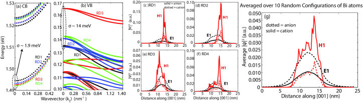
Fig. 1 plots the calculated dispersion of (a) the conduction bands (CB) and (b) the valence bands (VB) along the [110] direction ( = ; ). We show the lowest two conduction bands and the highest few valence bands close to the -point for four different random distributions of the Bi atoms in the QW (labelled as RD1, RD2, RD3, and RD4). The alloy disorder only negligibly affects the CB dispersion; the lowest CB energies for the four random Bi atom distributions are within approximately 3 meV of each other. The calculated valence band dispersion is however significantly affected by the different random Bi distributions in the four cases shown in the figure, which introduce a large variation in the highest VB energy at the -point, as well as differences in the band dispersion for 0. The energy of the highest valence band state has a standard deviation of 14 meV computed from twenty simulations with different random distributions of Bi atoms in the supercell. Because Bi pairs and clusters introduce resonant states close to and slightly above the valence band of the host GaAs material Usman et al. (2011), variations in the Bi distribution in the different supercells have a much stronger impact on the valence band than on the conduction band.
The strong perturbation of the valence band states is also evident in probability density plots of the highest valence band states at the -point, computed for the four random distributions of Bi atoms, as shown in Fig. 1 (c-f). Here we plot, along the z-direction, the cumulative probability density summed over all atoms in the -plane at each -point. Separate plots are shown for the cation and anion planes. We find that the valence band states are strongly localized around clusters of Bi atoms, with the peaks in the probability density plots corresponding directly to the presence of either a pair or a higher order cluster in that -plane. Conversely, the electron probability density variation is well described using a smooth envelope function, being largely unaffected by random variations in the local distribution of Bi atoms. To further average out the effect of variations in the Bi configurations, we plot in Fig. 1 (g) the electron and hole probability densities computed from the average of ten different random distributions of Bi atoms. The plots clearly exhibit that a noticeable distortion of the valence band states is still present even in the averaged plots, confirming that the random alloy fluctuations have significant impact on the electronic and optical properties of the bismide QWs. This reinforces the importance of more detailed atomistic models such as the tight-binding approach applied here to properly understand the physics of GaBixAs1-x QW-based optoelectronic devices.
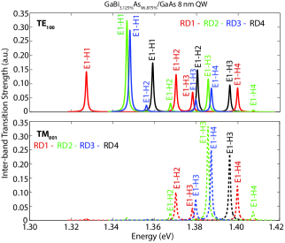
Fig. 2 plots the interband TE100 and TM001 squared optical transition matrix elements between the lowest electron state (E1) and the four highest hole states (H1 H4) for the four 8 nm GaBixAs1-x single QWs ( = 3.125%) considered in Fig. 1, computed from equations 4 and 5 respectively. Each electron-hole optical transition strength is artificially broadened by multiplying it by a Lorentzian function of 0.5 meV full-width-half-maximum, and with the peak centered at the energy of the optical transition (E1-H, ). The alloy disorder effects introduce large modifications not only in the energy but also in the TE100 transition strength for the ground state E1-H1 transition. Based on twenty different randomly distributed Bi atom calculations, we calculate an inhomogeneous broadening in the FWHM of the TE100-related band edge transition energy of 33 meV for the E1-H1 transition at 3.125% Bi in the QW, which is in good agreement with the large broadening observed in photoreflectance measurements Usman et al. (2013) and in recent photo-voltage measurements performed on GaBixAs1-x QW devices Broderick et al. (2014). We find that the lower hole states (H2, H3, and H4) also contribute sizeable TE100 strength, further adding to the broadening of the TE100 absorption edge. This is contrary to what would be expected based on a standard envelope function model, where several of the observed transitions would be expected to be symmetry forbidden. We note for instance for the random distribution of Bi atoms RD4 that the E1-H1 and E1-H2 TE100 transitions are of comparable magnitude, even though H1 and H2 are heavy-hole-like states. It can be seen however from Fig. 1 that the random Bi distribution breaks the expected even symmetry of the highest valence state; the reduced symmetry of the valence states then allows transitions between the lowest conduction state and a wider range of valence states, adding further to the inhomogeneous broadening of the band edge transition. The TM001 mode computed from only the highest four valence band states appears to be relatively less broadened; we note however that the LH character is spread over many valence band states Usman et al. (2013) so that a larger number of valence band states would need to be included in the calculation to compute the full width of the TM mode transition.
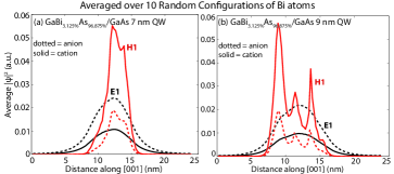
In order to investigate the effect of variations in the QW width, we also simulate GaBixAs1-x QWs ( = 3.125%) with 7 nm and 9 nm widths. Fig 3 plots the electron and hole probability densities along the direction, summed over all the atoms in the -plane at each point, for (a) 7 nm and (b) 9 nm QW widths. Each plot is averaged over ten random distributions of Bi atoms. These plots, along with the 8 nm QW plots previously shown in Fig. 1 (g), demonstrate an increasing impact of alloy disorder on the valence band envelope function (H1) as the QW width is increased from 7 nm to 9 nm. To further check this result, we also increased the in-plane supercell size from 4 nm to 8 nm for the three different QW widths (7 nm, 8 nm, and 9 nm); the results confirmed the same trend in the disorder-induced distortion of the valence band states. By contrast, the electron wave functions remain largely unaffected by the QW width variations, and continue to be well described using an envelope function approach.
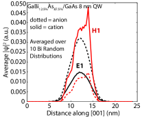
Experimental and theoretical analysis shows that above 10% Bi composition, the spin-orbit-splitting energy exceeds the band gap energy Usman et al. (2013); Batool et al. (2012), which should lead to the suppression of the CHSH Auger recombination loss mechanism that is the dominant efficiency-limiting process in conventional telecom lasers Broderick et al. (2012). From the device performance perspective, analysis of QW devices containing more than 10% Bi is of great interest. We therefore next simulate GaBixAs1-x QW structures with 12.5% Bi, corresponding to 512 Bi atoms randomly placed at As sites in the QW region. In order to study the influence of alloy disorder effects on the confined electron and hole states at 12.5% Bi fraction, we again simulate ten different random distributions of Bi atoms and plot the average electron and hole probability densities in cation and anion planes along the direction in Fig 4. The lowest electron wave function (E1), as in the case of 3.125% Bi composition, is well described by a smoothly varying envelope function. The averaged highest hole state (H1) probability density again deviates from that expected using an envelope function model, but the deviation is smaller than that obtained for the =3.125% case shown earlier in Fig. 1 (g).
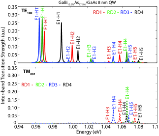
Similar trends are observed in Fig. 5 where we plot the TE100 and TM001 optical transition strengths for the 12.5% GaBixAs1-x QW and for four different random distributions of Bi atoms (RD1, RD2, RD3, and RD4). In comparison to the =3.125% QW (shown earlier in Fig. 2), the TE100 transitions are spread over a smaller energy range, exhibiting a reduced inhomogeneous broadening in the FWHM of 23.5 meV for the E1 to H1 transitions. The lower hole states (H2 H5) also contribute in the TE100 spectra, but with a weaker contribution than in the =3.125% case. The TM001 transitions are also considerably suppressed and broadened compared to the =3.125% case. These results indicate that pair and cluster related disorder has a lesser impact on the TE100 transitions at higher bismuth compositions, while the opposite is true for the TM001 transitions. This is in agreement with our earlier analysis of strained bulk GaBixAs1-x Usman et al. (2013) where at large Bi fraction ( = 10.4%), the HH-related transition was cleanly observed in the photo-modulated reflectance (PR) measurements, whereas the LH-related transition was strongly smeared out and difficult to identify when fitting to the PR spectra.
In conclusion, we have undertaken large supercell calculations using the tight-binding method to investigate the electronic and interband optical properties of GaBixAs1-x single QWs including the effect of random alloy fluctuations. We find that the conduction band states are largely unaffected by alloy disorder, but that even random variations in the Bi distribution have a strong impact on the valence band states, introducing a large inhomogeneous energy broadening and significantly distorting the confined state wave functions, in particular at lower Bi composition. The inhomogeneous broadening in the FWHM of the E1-H1 optical transition is calculated to be 33 meV at 3.125% Bi which reduces to 23.5 meV for 12.5% Bi in the QW region. Furthermore, the symmetry breaking allows transitions between the lowest conduction band state and a wide range of valence band states, leading to a further contribution to the inhomogeneous broadening of the absorption spectra. We also calculate that the disorder related effects are stronger for larger QW widths. Overall, our calculations emphasise the importance of taking alloy disorder effects into account for the analysis and design of optoelectronic devices based on this new class of III-V materials.
This work is supported by the European Union Seventh Framework Programme (BIANCHO; FP7-257974). The authors thank C. A. Broderick for useful discussions. M.U. acknowledges the use of computational resources from nanoHub.org (Network for Computational Nanotechnology, Purdue University).
References
- Sweeney (2010) S. J. Sweeney, Patent WO2010149978 (2010).
- Sweeney et al. (2011) S. J. Sweeney, Z. Batool, K. Hild, S. R. Jin, and T. J. C. Hosea in Proceedings of the 13th International Conference on Transparent Optical Networks (ICTON), Stockholm, Sweden, 2011.
- Li and Wang (2013) H. Li and Z. M. Wang, Bismuth-Containing Compounds (Springer New York, 2013).
- Usman et al. (2011) M. Usman, C. A. Broderick, A. Lindsay, and E. P. O’Reilly, Phys. Rev. B 84, 245202 (2011).
- Batool et al. (2012) Z. Batool, K. Hild, T. J. C. Hosea, X. Lu, T. Tiedje, and S. J. Sweeney, J. Appl. Phys. 111, 113108 (2012).
- Broderick et al. (2012) C. A. Broderick, M. Usman, S. J. Sweeney, and E. P. O’Reilly, Semicond. Sci. Technol. 27, 094011 (2012).
- Ludewig et al. (2013) P. Ludewig, N. Knaub, N. Hossain, S. Reinhard, L. Nattermann, I. Marko, S. Jin, K. Hild, S. Chatterjee, W. Stolz, S. Sweeney, and K. Volz, Appl. Phys. Lett. 102, 242115 (2013).
- Imhof et al. (2010) S. Imhof, A. Thranhardt, A. Chernikov, M. Koch, N. S. Koster, K. Kolata, S. Chatterjee, S. W. Koch, X. Lu, S. R. Johnson, D. A. Beaton, T. Tiedje, and O. Rubel, Appl. Phys. Lett. 96, 131115 (2010).
- Gogineni et al. (2013) C. Gogineni, N. A. Riordan, S. R. Johnson, X. Lu, and T. Tiedje, Appl. Phys. Lett. 103, 041110 (2013).
- Shan et al. (1999) W. Shan, W. Walukiewicz, J. W. A. III, E. E. Haller, J. F. Geisz, D. J. Friedman, J. M. Olson, and S. R. Kurtz, Phys. Rev. Lett. 82, 1221 (1999).
- Usman et al. (2013) M. Usman, C. A. Broderick, Z. Batool, K. Hild, T. Hosea, S. Sweeney, and E. P. O’Reilly, Phys. Rev. B 84, 245202 (2013).
- Klimeck et al. (2007) G. Klimeck, S. Ahmed, N. Kharche, M. Korkusinski, M. Usman, M. Prada, and T. Boykin, IEEE Trans. Elect. Dev. 54, 2090 (2007).
- Broderick et al. (2014) C. A. Broderick, P. Harnedy, P. Ludewig, Z. Bushell, K. Volz, and E. P. O’Reilly, “Determination of band offsets in GaBiAs/AlGaAs quantum wells using polarization resolved photovoltage spectroscopy and 12-band k.p calculations,” in preparation (2014).