2. Tokyo Metropolitan University, 3. ISAS/JAXA, 4. SRON,
5. Seiko Instruments Inc, 6. Hitachi High-Tech Science Corporation
11email: yamada@crab.riken.jp
Development of Multilayer Readout Wiring TES Calorimeter for Future X-ray Missions
Abstract
We have fabricated multilayer readout wiring Transition Edge Sensors (TES), which enable us to realize both large effective area and high-energy resolution for future X-ray astrophysical missions, such as DIOS. By sandwiching a SiO2 insulation layer between Al superconducting signal and return lines, self/mutual inductances and self fielding of bias leads are expected to be reduced. We fabricated 44 and 2020 TES array on the multilayer wiring and tested their performance. Under the low temperature condition, several pixels in the TES array showed sharp superconducting transitions at around 300 mK. We also succeeded in detecting X-ray signals from the 44 TES, contrary to the previous results of 2020 TES. We further investigated the reasons for the differences between the 44 TES and the 2020 TES, and present future plans for improving the multilayer TES array fabrication.
Keywords:
TES, X-ray astronomy, multilayer wiring1 Introduction
Microcalorimeters, which use small temperature rise ( 0.001 K) to measure deposited energy, are now becoming the most promising and standard detector for the next-generation X-ray astronomical mission, such as Micro-X (Figueroa-Feliciano et al. 20081), ASTRO-H SXS (Takahashi et al. 20102) and AXSIO (Bookbinder et al. 20123). Among several types of microcalorimeters, the most-established in the X-ray band is the Transition-Edge Sensor (TES) thermometer which consists of thin-films electrically biased in the superconducting-to-normal transition where electrical resistance significantly depends on temperature45.
The Japanese future small satellite mission carrying TES calorimeters is Diffuse Intergalactic Oxygen Surveyor (DIOS; Ohashi et al. 20106), aiming for detecting Warm-Hot Intergalactic Medium7. In space application of TES used together with X-ray mirrors, maximizing X-ray absorber area per given detector area on a focal plane is crucial. To realize mission requirement for the wide field of view, 150 cm2 deg2, we have been developing multi-layer wiring TES calorimeter (Ezoe et al. 20098 and 20129, Oishi et al. 201210), based on our standard coplanar-type TES118.
One of the multi-layer wiring TES Array (TESA) consists of hot (top layer) and return (bottom layer) wires passing parallel to the insulated layer of SiO2, so that wires can be more tightly packed than coplanar wiring, also making opening angle wider, as well as reducing cross talks between wires; cf., Chervenak et al. 201213. We designed the multi-layer wiring 2020 pixel TES and studied its basic properties9, but could not obtain an anticipated performance. We therefore assessed the performance of 44 pixel TESA with multi-layer wiring, and compared the results between the 44 TESA and the 2020 TESA.
2 Design of Multi-layer Readout Wiring TES
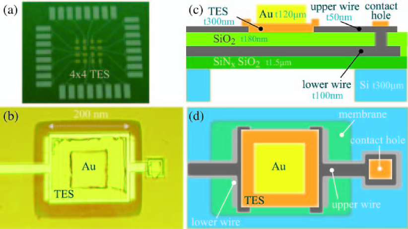
We fabricated a 44 TESA on top of the multi-layer wiring. Figure 1 shows an overall picture and a closed-up one of the TES. Upper (bias) and lower (return) wiring made of Al sandwiches an insulation SiO2 film, and are linked through a contact hole9. Ti and Au TES layers are 200 m on a side by 100 nm and 200 nm thick, respectively. Au Absorber is 120 m on a side by 1.7 m thick; upper and lower wire widths are 20 m and 30 m; and heights are 50 nm and 100 nm, respectively. Process yield in terms of electrical resistance at room temperature were estimated to be 95%10, which were measured by tossing the tips of the manual prober onto each boding pad at room temperature.
3 Experimental Results
3.1 Setup and Basic properties
We used the dilution refrigerator (OXFORD Kelvinox25) in Tokyo Metropolitan University, which has 25 W cooling power with a lowest-achievable temperature of 50 mK. The 44 TES shown in figure 1 is placed on the detector stage with a RuO2 thermometer which is read out and controlled by Picowatt AVS47/TS-530. On top of the TES, 55Fe isotopes is mounted as X-ray sources. One of the TES pixel with Au absorber out of 8 pixel is voltage-biased and lined to SQUID readout.
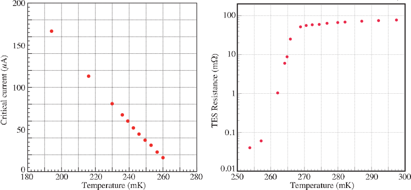
We measured the critical current () and TES resistance as a function of temperature at the detector stage, as shown in figure 2. The transition temperature () was 265 mK, which is expected from this TES thicknesses; for example, Ti and Au thickness of our coplanar-type TES were 40 nm and 80 nm, respectively. We could expect to obtain lower than 265 mK when the TES thicknesses are optimized.
As the temperature is reduced, increases, expected from the GL theory. The TES resistance ranges from 0.28 m (super), which is consistent with zero within error of the measurement, through 153 m (normal). The obtained residual resistance became lower than 20 m obtained from the 2020 pixel TES9, which was presumably due to remaining materials on the TES. Our coplanar TES measured by Ishisaki et al. 200714 showed that was larger than 100 A at 90% normal resistance, suggesting that of the multi-wiring TESA is increased by reviewing cleaning processes.
3.2 X-ray Irradiation
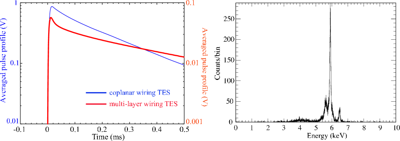
We proceeded to measure the X-ray spectrum of the multi-layer wiring TES. The thermal bath temperature is set at 185.5 mK with a bias voltage of 2.4 V, in order to operate the TES under electro-thermal feedback working. We succeeded in obtaining X-ray signal and the pulse profile averaged over all the X-ray signals during the entire measurement ( 10 h) is shown in figure 3 (left). The pulse profile of the coplanar wiring TES11 is overlaid, which is taken under the same configuration. Apparently, the height of the pulse differs by an order of magnitude. The time constants in the multi-layered wiring TES seem to be a sum of fast ( 0.02 ms) and slow ( 0.2 ms) falling components, while the fast one is less obvious in the coplanar TES. We evaluated the baseline fluctuation by using off-source data, and found it to be 40 eV.
We created optimal filter by collecting X-ray event data and off-source data, and then corrected the raw pulse height data for temperature-dependent fluctuation by aligning the Mn Kα1 peak. The obtained spectrum is presented in figure 3 (right). The energy resolution is 100 eV at 5.9 keV, which would be probably due to its quite low pulse height, or might be related to thick TES layers causing the high transition temperature.
4 Discussion and Conclusion
We compared 44 TESA obtained in this proceeding with 2020 TESA properties9. The obtained results are summarized in table 1.
| yield rate | @0.9 | (super) | (normal) | |||
|---|---|---|---|---|---|---|
| 44 TES | 94% | 260 mK | 100A | 0.28 m | 153 m | 100 eV |
| 2020 TES | 60% | 245 mK | 4A | 20 m | 9 | - |
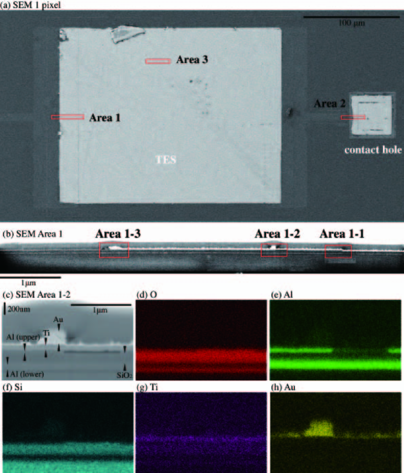
To further study these differences, we scrutinized cross-sectional views of the 2020 TES by using Scanning Electron Microscope (SEM) and Focusing Ion Beam (FIB) with Energy Dispersive X-ray Spectrometer (EDS). Figure 4a shows a top view of SEM picture taken from one pixel of the 2020 TES, where we marked three portions according to our interest: the junction between Al wire and TES (Area 1), the contact hole (Area 2), and the middle portion of the TES (Area 3). In the latter two parts, the TES layers and wires showed good homogeneity and adhesiveness.
There was, however, found serious issues in Area 1. Figure 4b shows the cross-sectional view of the multi-layer wiring TES pixel of Area 1; furthermore, SEM and EDS pictures in Area 1-2 are shown in figure 4c–4h. This portion should have maintained Al-upper wire by 100 nm thick and Au (TES) by 250 nm thick, though the Al-upper wire seems to have huge void (figure 4e) and the Au layer are far thinner than 250 nm (figure 4h). To identify a fabrication process that affected these features, we made another multi-layer wiring 2020 TES pixels, and measured R-T curves for each process step. Eventually, we noticed that normal resistance increased from 100 m to after TES pattering process. Therefore, it is likely that something during TES patterning might affect the lack of Al and Au. One of the key countermeasures is to make the TES layer thinner while the Al layer thicker. As a next step, we are trying to fabricate taper-shaped Al upper wires, because smooth edges of Al wire make heights of TES layers shorter, while the hight of Al higher, presumably making the transition temperature lowered and the contact between TES with Al wires more smooth and robust, resulting in better energy resolution and anticipated superconducting behavior.
In summary, we have successfully obtained X-ray signals from the 4x4 pixel multi-layer readout TES, in order to fabricate large array TES used for the future X-ray missions, such as DIOS. We found that some of fabrication processes that worked for 4x4 TES were not directly applicable to the 20x20 TESA.Further improvement are still underway, including changing edge shape of Al wires.
Acknowledgements.
The author would like to thank for many students involved in this work. The research presented here has been financed by the Special Postdoctoral Researchers Program in RIKEN and JSPS KAKENHI Grant Number 24740129.References
- 1 E. Figueroa-Feliciano, et al., in Proc. SPIE, 2008, vol. 7011, p. 70113U
- 2 Takahashi, T., Mitsuda, K., Kelley, R., et al.., Proc. SPIE, 7732, 2010
- 3 Bookbinder, J. A., Smith, R. K., Bandler, S., et al., SPIE, 8443, 17, 2012
- 4 K. D. Irwin and G. C. Hilton, Topics Appl. Phys., vol. 99, p.63, 2005
- 5 S. J. Smith, et al.,J. Low Temp. Phys., vol 167, 168, 2012
- 6 T. Ohashi, et al., in Proc. SPIE, 2010, vol. 7732, p.77321S
- 7 Yoshikawa et al., Astrophysical Journal, 558, 520, 2001
- 8 Y. Ezoe, et al., in AIP Conf. Proc., 2009, vol 1185, 60
- 9 Y. Ezoe, S. Oishi, S. Yamada, et al., IEEE Trans. Appl. Super., 23, 3, 2012
- 10 S. Oishi, Y. Ishisaki, Y. Ezoe, et al., J. Low Temp. Phys., vol 167, 220, 2012.
- 11 H. Akamatsu, et al., in AIP Conf. Proc., 2009, vol1185, 195
- 12 Y. Ezoe, et al., IEEE Trans. Appl. Supercond., vol21, 246, 2011
- 13 J.A. Chervenak, et al., J. Low Temp. Phys., vol 167, 547, 2012
- 14 Y. Ishisaki, H. Kurabayashi, et al., J. Low Temp. Phys., vol 151, 1, 131, 2007.