Coherent spin transport and suppression of spin relaxation in InSb nanowires with single subband occupancy at room temperature
Abstract
A longstanding goal of spintronics is to inject, coherently transport, and detect spins in a semiconductor nanowire where a single quantized subband is occupied at room temperature. Here, we report achieving this goal in 50-nm diameter InSb nanowires by demonstrating both the spin-valve and the Hanle effect. The spin relaxation time in the nanowires was found to have increased by an order of magnitude over what has been reported in bulk and quantum wells due to the suppression of D’yakonov-Perel’ spin relaxation as a result of single subband occupancy. These experiments raise hopes for the realization of a room-temperature Datta-Das spin transistor.
pacs:
72.25.Dc, 72.25.Hg, 72.25.RbTwo phenomena that unambiguously demonstrate injection, coherent transport and detection of spins in a solid are the spin-valve effect and the Hanle effect. In the former effect, the magnetoresistance of a trilayered structure, consisting of a paramagnet interposed between two ferromagnets that inject and detect spins, exhibits either a peak or a trough between the coercive fields of the two ferromagnets julliere . In the latter effect, the conductance of the structure exhibits periodic oscillations in a magnetic field that is non-collinear with the magnetizations of the two ferromagnets. Both effects have been observed simultaneously at low temperature lou and room temperature kum , but in systems where multiple quantized electron states (subbands) are occupied by electrons. Here, we report observing them in a solid where a single subband is occupied. Single subband occupancy is important for two reasons; it allows complete suppression of the dominant spin relaxation mechanism (D’yakonov-Perel’) in most semiconductors dyakonov ; holleitner ; pramanik1 and it also eliminates wavevector dependence of the spin precession thereby nullifying the deleterious effects of ensemble averaging at a finite temperature. As a consequence, a Datta-Das spin transistor datta , implemented with a single subband occupied quantum wire channel, can ideally produce infinite conductance on/off ratio at room temperature. No other structure can do this.
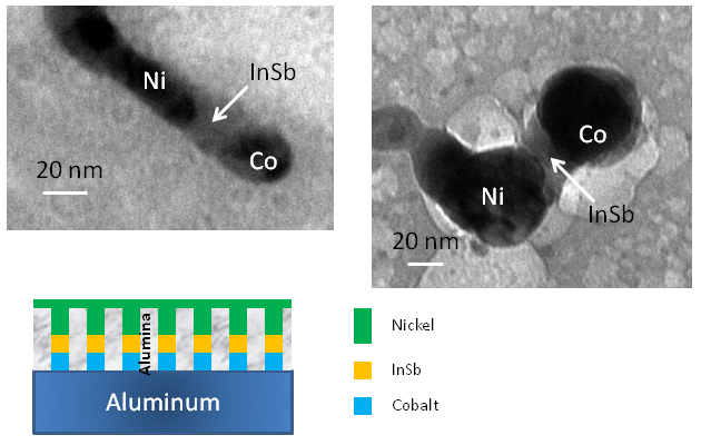
Parallel arrays of trilayered nanowires, each of 50 nm diameter and consisting of Co, InSb and Ni layers, were fabricated by sequentially electrodepositing Co, InSb and Ni in 50-nm diameter pores of nanoporous anodic alumina films. Details of fabrication are given in the supplementary material. Each nanowire is a “spin-valve”; one ferromagnetic contact injects spin-polarized electrons via tunneling through the Schottky barrier formed at the ferromagnet/semiconductor interface, and the other ferromagnetic contact transmits the electrons to varying degrees depending on their spin polarization. Thus, the injecting contact acts as a spin polarizer and the detecting contact acts as a spin analyzer. In each nanowire, 96% of the electrons occupy the lowest subband at room temperature (see supplementary material) so that there is essentially single subband occupancy. Approximately 108 parallel wires are electrically contacted from the top and bottom, forming an assembly of 108 parallel resistors. A schematic of the structure is shown in the inset of Fig. 1 which shows a transmission electron micrograph of a single trilayered nanowire that formed within the pores. Energy dispersive analysis of x-ray (EDAX) spectra of the samples are shown in the supplementary material. Cross-section scanning electron micrographs of similar structures can be found in ref. [saumil, ], showing the wires’ geometry.
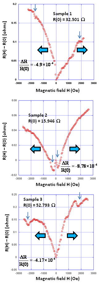
Longitudinal magnetoresistance (magnetic field directed parallel to wire axes) plots were obtained for three different samples at room temperature and are shown in Fig. 2. Each sample exhibits a clearly discernible trough in the magnetoresistance during both forward and reverse scans of the field. In samples 1 and 3, the troughs occur at magnetic fields that are consistent with coercivity values reported in the literature for cobalt and nickel nanowires produced in anodic alumina pores zeng ; zheng . This confirms that the troughs are indeed due to the spin-valve effect alphenaar . In sample 2, however, the troughs occur at very low fields, which can only happen if the coercivity of the nickel layer has dropped 30-fold to 50 Oe. This low coercivity may be due to excessive overfilling of the anodic alumina pores during nickel electrodeposition, resulting in the formation of a thick nickel layer on the surface that behaves like bulk instead of a nanowire. The coercivity of bulk nickel is only 20 Oe geiss . Scanning electron microscopy confirmed that indeed this had happened in some samples (see supplementary material).
Observation of the spin valve effect establishes successful injection, coherent transport and detection of spins at room temperature. Since cobalt and nickel both have negative spin polarizations tsymbal , one would have expected the spin-valve effect to produce a magnetoresistance peak instead of a trough. In reality, what we are observing here is the inverse spin valve effect that has been seen before and explained tsymbal1 ; pramanik . The sign inversion of the peak (which makes it a trough) is believed to be caused by electrons resonantly tunneling through one or more localized defect sites in the InSb spacer layer whose energies match the Fermi energy of the ferromagnetic electrodes. This effectively inverts the spin polarization of the ferromagnet closer to the defect site tsymbal1 . Such behavior has been observed previously in ferromagnetic/paramagnetic nanojunctions of cross section smaller than 0.01 grown by electrodeposition, as is the case here tsymbal1 .
Each plot in Fig. 2 shows a monotonically increasing background magnetoresistance. This is expected in narrow gap semiconductors like InSb owing to the strong non-parabolicity of the conduction band aurora . In the case of sample 1, however, there was also a thermal drift in the resistance due to sample heating by the current, which contributes part of the observed background magnetoresistance. No such drifts were observed in samples 2 and 3.
One can relate the magnitude of the trough to the spin relaxation length in the InSb spacer layer by invoking the modified Julliere formula vardeny which is
| (1) |
where is the resistance of the structure at zero magnetic field, and are the spin polarizations of the two magnetic contacts, is the separation between the contacts and is the spin relaxation length.
In our nanowires, 96% of the electrons reside in the lowest subband and hence we have almost a true one-dimensional system (see Sections S6 and S7 of the supplementary material for theoretical and experimental substantiation of single-subband occupancy). Therefore, we can write and , where is the drift velocity of electrons, is the ensemble averaged transit time and is the ensemble averaged spin relaxation time. This reduces Equation (1) to
| (2) |
The spin polarizations in bulk nickel and cobalt at 0 K have been reported as 0.33 and 0.42, respectively tsymbal , but at room temperature, the value reported in 50 nm thin films of cobalt is only 0.1 jedema2 . There is one report that the value increased to 0.16 when the resistance of the junction between cobalt and a non-magnetic spacer increased tinkham , but this is not relevant to our work. Furthermore, interface effects always reduce spin polarization dowben , and we have a very large interface-to-volume ratio in our cobalt nanocontacts. Therefore, it is reasonable to expect that the spin polarization in our cobalt nanocontacts is no more than 0.1. There is no equivalent study for nickel, but we will assume a similar 4-fold reduction in the spin polarization and take it to be no more than 0.075 in the nickel nanocontacts. Based on these spin polarization values and the measured resistance ratio , we infer that the ratio is no more than 3.4 in sample 1, 2.8 in sample 2 and 3.6 in sample 3 at room temperature.
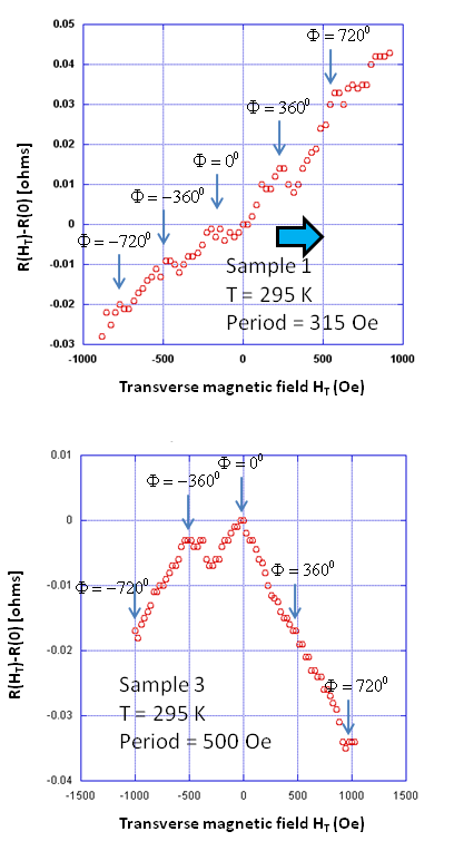
The transverse magnetoresistances of the samples are then measured in a magnetic field perpendicular to the axes of the wires. As long as this perpendicular field does not exceed the coercivities of the cobalt and nickel nanocontacts, the contacts will continue to inject and extract spins polarized parallel to the wire axis. These spins will precess about the perpendicular field while traversing the InSb layer. If the angle by which the majority spins precess in transiting the InSb layer is an odd multiple of 180∘, they will be transmitted since the spin polarizations of the two contacts are effectively opposite in sign (spin valve ‘trough’). On the other hand, if the angle is an even multiple of 180∘, the majority spins will be blocked. Hence, the resistance of the sample will oscillate periodically as the transverse magnetic field is scanned since the angle of precession is proportional to the transverse field. This is the well-known Hanle effect jedema2 ; takamura ; appelbaum ; fukuma . The period of the oscillation in magnetic flux density should be , where is the Bohr magneton and is the Landé g-factor of the spacer material (InSb).
In Fig. 3, we show the transverse magnetoresistance plots of samples 1 and 3 at room temperature. The transverse magnetic field strength is kept well below the coercivities of the cobalt and nickel nanocontacts (estimated from the longitudinal magnetoresistance plots in Fig. 2) in order to avoid flipping their magnetizations. Hence, their magnetizations remain parallel to the wire axis and they continue to inject and detect majority spins with polarization along the wire axis which is perpendicular to the applied field.
In sample 1, there is a distinct periodic oscillation in the resistance or conductance (equally spaced minima and equally spaced maxima) with a period of 315 Oe. This is the signature of the Hanle effect. In the case of sample 3, the oscillation is more muted, but there is still a hint of oscillation with a period of 500 Oe. Sample 2 did not show any oscillation since the coercivity of its nickel contact is too low for the observation of the Hanle effect. The oscillations are clearly non-sinusoidal because different nanowires produce slightly different periods, and ensemble averaging over the periods distorts the shape of the oscillation, making it appear non-sinusoidal.
There are two sources that introduce a spread in the transit time and hence a spread in the period of the Hanle oscillation. The first is inhomogeneous broadening due to a spread in the spacer layer width among the different nanowires, and the second is homogeneous broadening due to a spread in the electron velocity even within the same nanowire. As long as the distribution in the spacer layer width and carrier velocity (and hence the distribution in the period) is somewhat peaked, we will be able to observe a periodic behavior (with the period corresponding to the peak in the distribution), but the oscillation will be non-sinusoidal. In other words, successive minima and maxima will be equally spaced in the magnetic field, but the minima may not occur exactly midway between two successive maxima and vice versa. This is precisely what we see. The homogeneous broadening is fortunately small and the spread in velocity is much less than the thermal spread since electrons resonantly tunnel through one or more defect sites (which is why we observe the inverse spin valve effect) and resonant tunneling acts as a velocity filter. Only electrons whose energies are very close to the resonant level can tunnel through, which reduces the spread in kinetic energy and electron velocity. Therefore, most of the spread in the oscillation period accrues from the inhomogeneous broadening. The variation in the spacer layer width is 25% - 35% (see supplementary material), which should result in a similar variation in the period. This variation distorts the oscillation, making it non-sinusoidal, but still discernible.
Notice that the Hanle oscillations are not symmetric about zero transverse magnetic field. This usually happens when the transverse magnetic field is slightly misaligned and not exactly perpendicular to the axis of the nanowire appelbaum_arxiv . In our samples, we can never align the magnetic field exactly perpendicular to every wire’s axis since the wires themselves are not exactly mutually parallel. Hence, we will always observe some symmetry-breaking. Note also that in sample 1, the zero-field resistance is not a maximum and that there is a shift. This happens when the magnetizations of the two contacts are not exactly collinear.
Both samples show a background transverse magnetoresistance. In the case of sample 1, the resistance increases with time due to thermal drift and hence increases as the magnetic field is scanned slowly from negative to positive values. In the case of sample 3, which had no thermal drift, the magnetoresistance is negative and it is most likely caused by increasing depopulation of the higher subbands as the transverse field is increased. The transverse field increases the energy separation between successive subbands and therefore increases the population of the lowest subband at the cost of higher subband populations. The lowest subband usually has the highest mobility since its wavefunction is peaked at the center of the nanowire. Thus, one expects a negative transverse magnetoresistance in a nanowire. In our samples, 96% of the electrons are already in the lowest subband and only 4% are in higher subbands, which should make this effect almost negligible. Since the magnetoresistance is only 0.05%, it is quite plausible that this tiny decrease in the resistance in the transverse field is a consequence of higher subband depopulation.
From the observed average period in the magnetic flux density, one can calculate the ensemble averaged transit time of electrons through the InSb spacer layer according to the relation
| (3) |
The g-factors of materials are known to change in nanostructures from the bulk value, but in InSb quantum dots, the g-factor has been reported to be 52 in the lowest subband nilsson , which is close to the bulk value of 51. Based on this, we calculate = 44 ps in sample 1 and 28 ps in sample 3. Therefore, the ensemble averaged spin relaxation time in samples 1 and 3 are at least 13 ps and 8 ps, respectively. Note that these are true transport spin lifetimes, since they are measured in a transport experiment. Previous measurements of spin lifetimes have been carried out with optical techniques and not transport methods litvinenko ; murzyn ; bhowmick , which may not yield the true transport lifetime.
The room temperature spin relaxation time in epilayers of InSb has been reported as low as 2.5 ps litvinenko and as high as 300 ps murzyn , but in quantum wells, it drops to 1.2 - 4.2 ps bhowmick . It has been suggested theoretically that intrinsic inversion symmetry breaking at the interfaces of a quantum well can decrease spin relaxation time by over an order of magnitude olesberg . The calculated spin relaxation time in InAs/GaSb quantum wells is only 0.9 ps olesberg . In InSb nanowires of 50 nm diameter, we will expect the spin relaxation time to be even shorter than in quantum wells because of the larger interface-to-volume ratio, and hence shorter than 1 ps at room temperature. Therefore, the measured relaxation times of 13 and 8 ps are roughly an order of magnitude longer than what is expected.
The electron drift mobility in the InSb nanowires was ascertained from TEM observation of the spacer layer width, measured sample resistance and transit time extracted from the measured Hanle period (see Section S3 of supplementary material). It was found to have degraded by four orders of magnitude from the value reported in bulk or quantum wells, presumably owing to severe interface roughness scattering brought about by the nanowires having a large interface-to-volume ratio. The mobility degradation should increase the Elliott-Yafet spin relaxation rate by four orders of magnitude compared to bulk or quantum wells since this rate is inversely proportional to mobility elliott . Yet, the spin relaxation rate had decreased by nearly one order of magnitude. This can only happen if: (1) Elliott-Yafet is not the dominant spin relaxation mechanism in bulk and quantum wells of InSb, but D’yakonov-Perel’ is (this was theoretically predicted in ref. [kim, ]), and (2) the D’yakonov-Perel’ mechanism has been suppressed or eliminated in the nanowires because of strictly one dimensional confinement of carrier motion resulting from single subband occupancy holleitner ; pramanik1 . In Section S6 of the supplementary material, we present calculations to show that we indeed have single subband occupancy in our nanowires, and in section S7 we show that the room temperature conductance can be used to estimate the number of occupied subbands and it is, again, indeed O(1).
In conclusion, we have demonstrated both the spin valve and the Hanle effect at room temperature in trilayered nanowires of Co-InSb-Ni, thereby demonstrating spin injection, coherent spin transport and spin detection in a semiconductor at room temperature. The material InSb has a strong Rashba coefficient rashba , which makes it an ideal candidate for the Datta-Das spin field effect transistor datta . This transistor requires a strictly one-dimensional channel with a single subband occupied for the strongest effect book ; hence, the demonstration of coherent spin transport in these single-subband-occupied InSb nanowires – where the D’yakonov-Perel’ spin relaxation has been suppressed – raises hopes for a room temperature device with significant conductance modulation.
This work is supported by the US National Science Foundation under grant CCF 0726373. The authors are indebted to Dr. Dmitry Pestov for help with EDAX.
References
- (1) M. Julliere, Phys. Lett. A 54, 225 (1975).
- (2) X. Lou, et al, Nature Phys. 3, 197-202 (2007).
- (3) H. Kum, J. Heo, S. Jahangir, A. Banerjee, W. Guo, and P. Bhattacharya, Appl. Phys. Lett. 100, 182407 (2012).
- (4) M. I. D’yakonov and V. I. Perel’, Sov. Phys. JETP 33, 1053 (1971).
- (5) A. W. Holleitner, V. Shi, R. C. Myers, A. C. Gossard and D. D. Awschalom, New J. Phys. 9, 342 (2007).
- (6) S. Pramanik, S. Bandyopadhyay and M. Cahay, IEEE Trans. Nanotech. 4, 2 (2005).
- (7) S. Datta and B. Das, Appl. Phys. Lett. 56, 665 (1990).
- (8) S. Bandyopadhyay, J. N. Mateo, S. Bandyopadhyay and G. Glaspell, Physica E 43, 1255 (2011).
- (9) H. Zeng, R. Skomski, Y. Liu, D. J. Sellmyer and S. Bandyopadhyay, J. Appl. Phys. 87, 4718 (2000).
- (10) M. Zheng, L. Menon, H. Zeng, Y. Liu, S. Bandyopadhyay, R. D. Kirby and D. J. Sellmyer, Phys. Rev. B. 62, 12282 (2000).
- (11) K. Tsukagoshi, B. W. Alphenaar and H. Ago, Nature (London) 401, 572 (1999).
- (12) R. H. Geiss and J. Silcox, J. Appl. Phys. 39, 982 (1968).
- (13) E. Y. Tsymbal, O. N. Mryasov and P. R. Leclair, J. Phys: Condens. Matt. 15, R109 (2000).
- (14) E. Y. Tsymbal, A. Sokolov, I. F. Sabirianov and B. Doudin, Phys. Rev. Lett. 90, 186602 (2003).
- (15) S. Pramanik, S. Bandyopadhyay, K. Garre and M. Cahay, Phys. Rev. B. 74, 235329 (2006).
- (16) V. K. Arora and M. Jaafarian, Phys. Rev. B. 13, 4457 (1976).
- (17) Z. H. Xiong, D. Wu, Z. V. Vardeny and J. Shi, Nature 427, 821 (2004).
- (18) F. J. Jedema, M. V. Costache, H. B. Heersche, J. J. A. Baselmans and B. J. van Wees, Appl. Phys. Lett. 81, 5162 (2002).
- (19) S. O. Valenzuela and M. Tinkham, Appl. Phys. Lett. 85, 5914 (2004).
- (20) P. A. Dowben and R. Skomski, J. Appl. Phys. 95, 7453 (2004).
- (21) Y. Takamura and S. Sugahara, J. Appl. Phys. 111, 07C323 (2012).
- (22) I. Appelbaum, B. Huang and D. J. Monsma, Nature 447, 295 (2007).
- (23) Y. Fukuma, L. Wang, H. Idzuchi, S. Takahashi, S. Maekawa and Y. C. Otani, Nature Mat. 10, 527 (2011).
- (24) J. Li, B. Huang and I. Appelbaum, Appl. Phys. Lett. 92, 142507 (2008).
- (25) H. A. Nilsson, P. Caroff, C. Thelander, M. Larsson, J. B. Wagner, L-E Warnersson, L. Samuelson and H. Q. Xu, Nano Lett. 9, 3151 (2009).
- (26) K. L. Litvinenko, L. Nikzad, B. N. Murdin, C. R. Pidgeon, J. J Harris, T. Zhang and L. F. Cohen, J. Appl. Phys. 101, 083105 (2008).
- (27) P. Murzyn, et al., Physica E 20, 220 (2004).
- (28) M. Bhowmick, R. N. Kini, K. Nontapot, N. Goel, S. J. Chung, T. D. Mishima, M. B. Santos and G. A. Khodaparast, Phys. Procedia 3, 1161 (2010).
- (29) J. T. Olesberg, W. H. Lau, M. E. Flatté, C. Yu, E. Altunkaya, E. M. Shaw, T. C. Hasenberg and T. F. Boggess, Phys. Rev. B. , 64, 201301(R) (2001).
- (30) R. J. Elliott, Phys. Rev. 96, 266 (1954).
- (31) P. H. Song and K. W. Kim, Phys. Rev. B 66 035207 (2002).
- (32) Y. A. Bychkov and E. I. Rashba, J. Phys. C: Solid State Phys. 17, 6039 (1984).
- (33) S. Bandyopadhyay and M. Cahay, Introduction to Spintronics (CRC Press, Boca Raton, 2008).