Superconducting nano-mechanical diamond resonators
Abstract
In this work we present the fabrication and characterization of superconducting nano-mechanical resonators made from nanocrystalline boron doped diamond (BDD). The oscillators can be driven and read out in their superconducting state and show quality factors as high as 40,000 at a resonance frequency of around 10 MHz. Mechanical damping is studied for magnetic fields up to 3 T where the resonators still show superconducting properties. Due to their simple fabrication procedure, the devices can easily be coupled to other superconducting circuits and their performance is comparable with state-of-the-art technology.
I Introduction
Nano-mechanical resonators allow to explore a variety of physical phenomena. From a technological point of view, they can be used for ultra-sensitive mass Yang et al. (2006); Jensen et al. (2008); Chaste et al. (2012), forceBraginskii and Manukin (1977); Ekinci and Roukes (2005); Moser et al. (2013), charge Steele et al. (2009); Lassagne et al. (2009) and displacement detection. On the more fundamental side, they offer fascinating perspectives for studying macroscopic quantum systems. Significant progress has been made in the last few years by cooling a nano-mechanical resonator into its ground state O Connell et al. (2010); Rocheleau et al. (2010); Teufel et al. (2011); Chan et al. (2011). Couplings between nano-mechanical resonators and superconducting circuits have been realized and even the creation of entanglement with these macroscopic oscillators seems in reach Walter et al. (2013). In order to exploit such a system in quantum information technology, nano-mechanical systems will have to be coupled to other quantum systems such as light Safavi-Naeini et al. (2013) or superconducting circuits O Connell et al. (2010); Armour et al. (2002); Naik et al. (2006); Regal et al. (2008); LaHaye et al. (2009); Suh et al. (2010) and new materials to improve the coupling for such hybrid systems are of importance. In this respect diamond is an extremely attractive material. Despite the fact that diamond has exceptional mechanical properties Wang et al. (2004); Gaidarzhy et al. (2007); Ovartchaiyapong et al. (2012); Najar et al. (2013), it has a relatively high refractive index which allows to couple it to light. In addition when doped with boron, it can be rendered superconducting with remarkable electrical properties and makes it a promising material for fully integrated hybrid nano-mechanical systems.
In this article we present the fabrication and characterization of nano-mechanical resonators built out of superconducting diamond. We demonstrate a simple top down process to fabricate these resonators by common electron beam lithography and hence offer a simple way to be implemented into superconducting circuits. We compare their performance to state-of-the-art resonators and investigate the limits of their superconductivity. Quality factors around 40000 at around 10 MHz resonance frequency are demonstrated and it is shown that it is possible to directly read out a superconducting resonator at a magnetic field as high as 3 Tesla.
II Fabrication
The nano-mechanical resonators have been fabricated from a superconducting nanocrystaline diamond film, grown on a silicon wafer with a 500 nm thick SiO2 layer. To be able to grow diamond on the Si/SiO2 surface, small diamond particles of a diameter smaller than 6 nm are seeded onto the silica substrate with the highest possible density Williams (2011). A subsequent microwave plasma chemical-vapor deposition (CVD) allows to grow and control various properties of the film. It is possible to vary the grain sizes from few nanometers to few microns by controlling the methane concentration. Furthermore one can add a variety of dopants to drastically change some of the key properties of pure diamond. While adding boron gas during the CVD process one can turn the elsewise insulating diamond film metallic and above a critical concentration even superconducting Ekimov et al. (2004); Bustarret et al. (2004). A detailed description of this growth process can be found in reference Williams (2011).
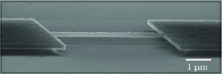
The nano-mechanical structures have been defined using standard electron beam lithography. First, a 70 nm thick nickel etch mask which defines the sample geometry has been evaporated on top of the diamond film which has then been followed by anisotropic oxygen plasma etching Mandal et al. (2011). The sample is cooled to 10oC while being exposed to the oxygen plasma for approximately 8 minutes. The anisotropy of the etching process leads to straight walls that broaden less than 5 nm after 300 nm of etching. After this process, the nickel mask is removed by dipping the sample in a FeCl3 solution. To provide good ohmic contacts, a tri-layer consisting of titanium, platinum and gold has been evaporated followed by annealing at 750oC. The structures have been suspended by etching the sacrificial SiO2 layer using HF vapor at 50oC and atmospheric pressure for about 10 minutes. Diamond itself is inert to this chemical etching process. Due to the strong mechanical stiffness, tri-critical point drying has not been necessary even for structures with lengths up to 30 micrometers. Figure 1 displays a suspended diamond structure that has been fabricated by this method. We have also fabricated superconducting diamond resonators that were covered with a 50 nm thick gold layer in order to test the samples at temperatures above the superconducting transition temperature and at currents above the superconducting critical current. This allows for easy detection of the resonance conditions. For this purpose a slightly modified technique was used. After the e-beam process a metallic bilayer of 50 nm gold and 50 nm of nickel was deposited instead of 70 nm nickel as in the previous case. This bilayer acts as a mask for the etching process. The nickel layer was subsequently removed using FeCl3 which does not attack the gold layer. Finally the combination of diamond and gold layer was exposed to HF gas for suspension. The etch rate of gold in HF at the temperatures used is negligible Williams et al. (2003).
In the following, we mainly discuss the results of two resonators, one with a geometry of 30 m x 480 nm (length x width) and one with 25 m x 350 nm with a 50 nm gold layer on the top, referred to as sample A and sample B, respectively. The thickness of the diamond film was estimated to 300 nm using an optical profilometer.
III Measurements
The low temperature characterization of the nano-mechanical beams was done using the magneto-motive detection scheme Cleland and Roukes (1996). The radio frequency signal from a network analyzer (Rohde - Schwarz ZVL-13) was fed into a coaxial line at the top of a 3He cryostat with a base temperature of 500 mK. The signal was delivered to the sample through two attenuation stages: 20 dB at 4.2 K and 20 dB at the 1.2 K stage. An ac-current flowing through the sample exposed to a perpendicular external magnetic field B induces a Lorentz force that actuates the beam and leads to a displacement of the nano-mechanical beam in plane to the diamond film. On resonance, the beam dissipates energy changing its impedance and resulting in a dip in the transmission signal. The transmitted signal is amplified at 4.2 K with a gain of approximately 50 dB (Caltech CITLF1 SN120) and fed into the input port of the network analyzer. The same electrical set-up also allows for characterization of the superconducting properties of the nano-mechanical resonators.
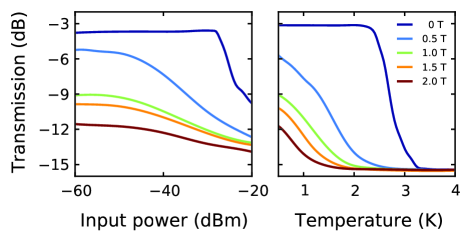
To verify whether our resonators show superconductivity, we first measured the superconducting transition as a function of the input power and temperature at a frequency of approximately 9 MHz close to the expected resonance frequency. The input power can in principle be directly converted into a current using a perfectly 50 Ohm adapted circuit model. However, since this approach neglects the change of sample impedance when sweeping through the resonance as well as contact resistances, it is more convenient to directly plot the input power instead of the bias current. Nevertheless, the calculated critical currents are of the order of few A, similar to what has been measured with DC measurements of similar nanostructures made from BDD Mandal et al. (2010a, b). The transmission signal of sample B is plotted in figure 2. One can clearly identify a constant transmission plateau at low input powers (left panel) and at low temperatures (right panel). A constant transmission directly goes with unaltered electrical properties for which we can identify the superconducting state of the beam. The device shows an increase in impedance at high input powers (temperatures), which leads to a reduction of the transmitted signal and eventually to the transition of the sample into its normal state. This impedance increase is associated with the absorption of microwave power. The splitting of cooper-pairs leads to the creation of excess quasiparticles and drastically alters the complex conductivity of our structure and hence the superconducting state de Visser et al. (2012).
From the total transmission drop we can calculate the approximate normal state resistance values to around 300 Ohms for sample B. We have obtained similar data for sample A and a normal state resistance close to 2.5 kOhm (not displayed). The difference in resistance is due to the presence of the gold layer on top of sample B. At higher magnetic fields, the superconducting transition is shifted to lower input powers and to lower temperatures and a residual resistance appears which can be associated to the increase of quasiparticles in the superconductor. We obtained a superconducting transition temperature of approximately 2.5 K at zero magnetic field in agreement with measurements on non-suspended diamond samples Mandal et al. (2011, 2010a, 2010b).
We now turn to the mechanical properties of the diamond nano-mechanical resonator. By applying a perpendicular magnetic field and sweeping the RF frequency of the bias, the resonators can be actuated and its characteristics can be extracted. In figure 3 we show a typical transmission signal at resonance obtained from sample A. The resonance frequency of resonator A and B are 9.39226 MHz and 8.77142 MHz respectively. Using
| (1) |
with being a numerical factor for the beams’ first flexual mode Cleland (2003), being its moment of Inertia, w its width, l its length and the density of diamond, we can calculate the Young’s modulus to 950 and 810 GPa, respectively. The difference between the Young’s moduli of sample A and B is simply due to the additional metal layer of the latter. In addition, the fact that the Young’s modulus is as high as the one observed for undoped nanocrystalline diamond Williams et al. (2010); Hees et al. (2013) shows that the boron doping does not degrade the mechanical properties.
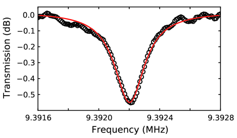
From the transmission measurement we can also extract the loaded quality factor Q, which describes the rate of energy loss, compared to the energy stored in the resonator. For sample A and B we find Q = 40000 and Q = 30000, respectively. From these measurements we conclude that the Young’s modulus as well as the quality factor of sample B is lower due to enhanced losses caused by the gold layer on top of the structure. The effect of the gold layer is to modify the mechanical properties in terms of surface stress, additional mass, additional elasticity and damping. Such effects have been studied in detail in the literature Collin et al. (2010); Imboden et al. (2013a, b).
A side effect of the magneto-motive detection technique is the circulation of eddy currents inside the structure, which leads to an additional magnetic field that is opposed to the applied external magnetic field. This results in an additive force that is opposed to the beam movement and leads to another damping term QE that adds linearly to the intrinsic mechanical damping.
| (2) |
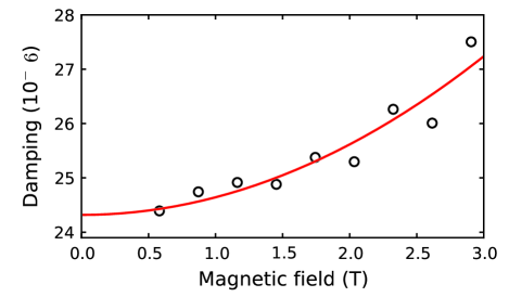
The eddy current damping Huang et al. (2005) scales with B2 and adds to the inverse of the intrinsic quality factor which is independent of the magnetic field and only depends on the intrinsic mechanical losses. Figure 4 shows the corresponding magnetic damping for sample A from which we extract the intrinsic unloaded quality factor Qmech = 41000 at zero magnetic field. This mechanical quality factor is limited by the surface roughness of the diamond and more importantly by clamping losses due to the doubly-clamped beam design. The isotropic etching of the sacrificial SiO2 layer leads to an undercut of the anchor pads of the NEMS. The more surface undercut the more dissipation is possible in the vibrating surroundings of the resonators’ clamps, the higher the losses. Possible solutions to increase this quality factor would be to use the so-called free-free beam design Huang et al. (2005), to reduce the surface losses by smoothing the surface with mechanical or chemical polishing before nanofabrication Thomas et al. (2014) and to remove the undercut by means of a focused ion beam technique. Nevertheless, the observed quality factors are comparable with state-of-the art resonators Ovartchaiyapong et al. (2012); Faust et al. (2012); Schmid et al. (2012). A commonly used value for comparison is the product of frequency and quality factor, fQ, for which we obtain 3.85 1011.
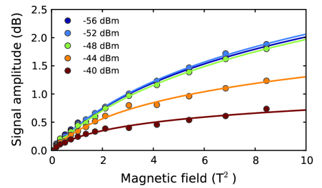
To convince oneself that the measured resonance is of mechanical nature and not of some electrical resonance, we plot the signal amplitude as a function of magnetic field in figure 5. Following Cleland and Roukes (1999), we can fit our curves using
| (3) |
where is the resonators impedance, adjusts the amplitude of the signal, is the line impedance and is a constant of order unity, depending on the mode shape Cleland and Roukes (1999).
The transmission signal of the resonator A shows a finite residual resistance at finite magnetic field as depicted in figure 2. This resistance can be seen as the real part of an external embedding impedance in series with the nano-mechanical oscillator. Assuming that this embedding impedance changes slowly over the resonance width which is justified in our case as the damping is low, we find that the loaded resonance frequency shifts according to Cleland and Roukes (1999)
| (4) |
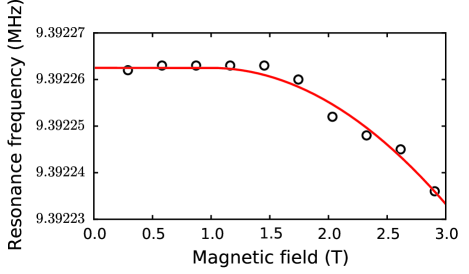
where is the unshifted frequency at zero embedding impedance. Assuming that the second term in equation 4 is zero below a critical field for the superconducting resonator we can fit our data of the resonance frequency shift as shown in figure 6. From the fit we extract the critical field to which is consistent with the onset of the residual resistance of sample A (not displayed).
IV Conclusion
We have demonstrated that nano-mechanical resonators made from boron doped diamond show superconducting properties up to magnetic fields of 3 Teslas. These resonators show high quality factors as high as 40000 at a resonance frequency of around 10 MHz. The simple fabrication process of superconducting diamond resonators allows for easy implementation into fully superconducting diamond circuits such as micro-cavities or superconducting quantum interference devices. Due to its remarkable mechanical, electrical as well as optical properties we conclude that nano-mechanical resonators made from boron doped diamond offer an extremely attractive system in the growing field of quantum opto-mechanics.
Acknowledgements.
C.B. acknowledges financial support from the French National Agency (ANR) in the frame of its program in Nanosciences and Nanotechnologies (SUPERNEMS project no anr-08-nano-033).References
- Yang et al. (2006) Y. T. Yang, C. Callegari, X. L. Feng, K. L. Ekinci, and M. L. Roukes, Nano Letters 6, 583 (2006).
- Jensen et al. (2008) K. Jensen, K. Kim, and A. Zettl, Nature nanotechnology 3, 533 (2008), ISSN 1748-3395.
- Chaste et al. (2012) J. Chaste, A. Eichler, J. Moser, G. Ceballos, R. Rurali, and A. Bachtold, Nature nanotechnology 7, 301 (2012), ISSN 1748-3395.
- Braginskii and Manukin (1977) V. B. Braginskii and A. B. Manukin, Measurement of weak forces in physics experiments (University of Chicago Press, Chicago, 1977), ISBN 0226070700 0226070700.
- Ekinci and Roukes (2005) K. L. Ekinci and M. L. Roukes, Review of Scientific Instruments 76, 061101 (pages 12) (2005).
- Moser et al. (2013) J. Moser, J. Guttinger, A. Eichler, M. Esplandiu, D. Liu, D. M.I., and A. Bachtold, Nat Nano 8, 493 (2013), ISSN 1748-3387.
- Steele et al. (2009) G. A. Steele, A. K. Hüttel, B. Witkamp, M. Poot, H. B. Meerwaldt, L. P. Kouwenhoven, and H. S. J. van der Zant, Science 325, 1103 (2009).
- Lassagne et al. (2009) B. Lassagne, Y. Tarakanov, J. Kinaret, D. Garcia-Sanchez, and A. Bachtold, Science 325, 1107 (2009).
- O Connell et al. (2010) A. D. O Connell, M. Hofheinz, M. Ansmann, R. C. Bialczak, M. Lenander, E. Lucero, M. Neeley, D. Sank, H. Wang, M. Weides, et al., Nature 464, 697 (2010), ISSN 0028-0836.
- Rocheleau et al. (2010) T. Rocheleau, T. Ndukum, C. Macklin, J. B. Hertzberg, A. A. Clerk, and K. C. Schwab, Nature 463, 72 (2010), ISSN 0028-0836.
- Teufel et al. (2011) J. D. Teufel, D. Li, M. S. Allman, K. Cicak, A. J. Sirois, J. D. Whittaker, and R. W. Simmonds, Nature 471, 204 (2011).
- Chan et al. (2011) J. Chan, T. P. M. Alegre, A. H. Safavi-Naeini, J. T. Hill, A. Krause, S. Groblacher, M. Aspelmeyer, and O. Painter, Nature 478, 89 (2011), ISSN 0028-0836.
- Walter et al. (2013) S. Walter, J. C. Budich, J. Eisert, and B. Trauzettel, Phys. Rev. B 88, 035441 (2013).
- Safavi-Naeini et al. (2013) A. H. Safavi-Naeini, S. Groblacher, J. T. Hill, J. Chan, M. Aspelmeyer, and O. Painter, Nature 500, 185 (2013), ISSN 0028-0836.
- Armour et al. (2002) A. D. Armour, M. P. Blencowe, and K. C. Schwab, Phys. Rev. Lett. 88, 148301 (2002).
- Naik et al. (2006) A. Naik, O. Buu, M. D. LaHaye, A. D. Armour, A. A. Clerk, M. P. Blencowe, and K. C. Schwab, Nature 443, 193 (2006), ISSN 0028-0836.
- Regal et al. (2008) C. A. Regal, J. D. Teufel, and K. W. Lehnert, Nat Phys 4, 555 (2008), ISSN 1745-2473.
- LaHaye et al. (2009) M. D. LaHaye, J. Suh, P. M. Echternach, K. C. Schwab, and M. L. Roukes, Nature 459, 960 (2009), ISSN 0028-0836.
- Suh et al. (2010) J. Suh, M. D. LaHaye, P. M. Echternach, K. C. Schwab, and M. L. Roukes, Nano Letters 10, 3990 (2010), eprint http://pubs.acs.org/doi/pdf/10.1021/nl101844r.
- Wang et al. (2004) J. Wang, J. Butler, T. Feygelson, and C.-C. Nguyen, in Micro Electro Mechanical Systems, 2004. 17th IEEE International Conference on. (MEMS) (2004), pp. 641–644.
- Gaidarzhy et al. (2007) A. Gaidarzhy, M. Imboden, P. Mohanty, J. Rankin, and B. W. Sheldon, Applied Physics Letters 91, 203503 (pages 3) (2007).
- Ovartchaiyapong et al. (2012) P. Ovartchaiyapong, L. M. A. Pascal, B. A. Myers, P. Lauria, and A. C. B. Jayich, Applied Physics Letters 101, 163505 (pages 4) (2012).
- Najar et al. (2013) H. Najar, A. Heidari, M.-L. Chan, H.-A. Yang, L. Lin, D. G. Cahill, and D. A. Horsley, Applied Physics Letters 102, 071901 (pages 4) (2013).
- Williams (2011) O. Williams, Diamond and Related Materials 20, 621 (2011), ISSN 0925-9635.
- Ekimov et al. (2004) E. A. Ekimov, V. A. Sidorov, E. D. Bauer, N. N. Mel’nik, N. J. Curro, J. D. Thompson, and S. M. Stishov, Nature 428, 542 (2004), ISSN 0028-0836.
- Bustarret et al. (2004) E. Bustarret, J. Kačmarčik, C. Marcenat, E. Gheeraert, C. Cytermann, J. Marcus, and T. Klein, Phys. Rev. Lett. 93, 237005 (2004).
- Mandal et al. (2011) S. Mandal, T. Bautze, O. A. Williams, C. Naud, E. Bustarret, F. Omnes, P. Rodiere, T. Meunier, C. Bäuerle, and L. Saminadayar, ACS Nano 5, 7144 (2011).
- Williams et al. (2003) K. Williams, K. Gupta, and M. Wasilik, Microelectromechanical Systems, Journal of 12, 761 (2003), ISSN 1057-7157.
- Cleland and Roukes (1996) A. N. Cleland and M. L. Roukes, Applied Physics Letters 69, 2653 (1996).
- Mandal et al. (2010a) S. Mandal, C. Naud, O. A. Williams, E. Bustarret, F. Omnes, P. Rodiere, T. Meunier, L. Saminadayar, and C. Bäuerle, Nanotechnology 21, 195303 (2010a).
- Mandal et al. (2010b) S. Mandal, C. Naud, O. A. Williams, E. Bustarret, F. Omnes, P. Rodiere, T. Meunier, L. Saminadayar, and C. Bäuerle, Physica Status Solidi (a) 207, 2017 (2010b), ISSN 1862-6319.
- de Visser et al. (2012) P. J. de Visser, J. J. A. Baselmans, S. J. C. Yates, P. Diener, A. Endo, and T. M. Klapwijk, Applied Physics Letters 100, 162601 (2012).
- Cleland (2003) A. N. Cleland, Foundations of Nanomechanics (Springer-Verlag Berlin Heidelberg New York, 2003).
- Williams et al. (2010) O. Williams, A. Kriele, J. Hees, M. Wolfer, W. M ller-Sebert, and C. Nebel, Chemical Physics Letters 495, 84 (2010), ISSN 0009-2614.
- Hees et al. (2013) J. Hees, N. Heidrich, W. Pletschen, R. E. Sah, M. Wolfer, O. A. Williams, V. Lebedev, C. E. Nebel, and O. Ambacher, Nanotechnology 24, 025601 (2013).
- Collin et al. (2010) E. Collin, J. Kofler, S. Lakhloufi, S. Pairis, Y. M. Bunkov, and H. Godfrin, Journal of Applied Physics 107, 114905 (2010).
- Imboden et al. (2013a) M. Imboden, O. A. Williams, and P. Mohanty, Nano Letters 13, 4014 (2013a).
- Imboden et al. (2013b) M. Imboden, O. Williams, and P. Mohanty, Applied Physics Letters 102, 103502 (2013b).
- Huang et al. (2005) X. M. H. Huang, X. L. Feng, C. A. Zorman, M. Mehregany, and M. L. Roukes, New Journal of Physics 7, 247 (2005).
- Thomas et al. (2014) E. L. Thomas, G. W. Nelson, S. Mandal, J. S. Foord, and O. A. Williams, Carbon 68, 473 (2014), ISSN 0008-6223.
- Faust et al. (2012) T. Faust, P. Krenn, S. Manus, J. Kotthaus, and E. Weig, Nat Commun 3, 728 (2012).
- Schmid et al. (2012) D. R. Schmid, P. L. Stiller, C. Strunk, and A. K. Hüttel, New Journal of Physics 14, 083024 (2012).
- Cleland and Roukes (1999) A. N. Cleland and M. L. Roukes, Sensors and Actuators A: Physical 72, 256 (1999), ISSN 0924-4247.