Random strain fluctuations as dominant disorder source for high-quality on-substrate graphene devices
Résumé
We have performed systematic investigations of transport through graphene on hexagonal boron nitride (hBN) substrates, together with confocal Raman measurements and a targeted theoretical analysis, to identify the dominant source of disorder in this system. Low-temperature transport measurements on many devices reveal a clear correlation between the carrier mobility and the width of the resistance peak around charge neutrality, demonstrating that charge scattering and density inhomogeneities originate from the same microscopic mechanism. The study of weak-localization unambiguously shows that this mechanism is associated to a long-ranged disorder potential, and provides clear indications that random pseudo-magnetic fields due to strain are the dominant scattering source. Spatially resolved Raman spectroscopy measurements confirm the role of local strain fluctuations, since the line-width of the Raman 2D-peak –containing information of local strain fluctuations present in graphene– correlates with the value of maximum observed mobility. The importance of strain is corroborated by a theoretical analysis of the relation between and that shows how local strain fluctuations reproduce the experimental data at a quantitative level, with being determined by the scalar deformation potential and by the random pseudo-magnetic field (consistently with the conclusion drawn from the analysis of weak-localization). Throughout our study, we compare the behavior of devices on hBN substrates to that of devices on SiO2 and SrTiO3, and find that all conclusions drawn for the case of hBN are compatible with the observations made on these other materials. These observations suggest that random strain fluctuations are the dominant source of disorder for high-quality graphene on many different substrates, and not only on hexagonal boron nitride.
I Introduction
Hexagonal boron nitride (hBN) substrates enable the fabrication of graphene devices Dean et al. (2010); Zomer et al. (2011); Mayorov et al. (2011); Wang et al. (2013), exhibiting extremely high carrier mobility values, and leading to the observation of new, interesting physical phenomena Dean et al. (2011); Young et al. (2012); Ponomarenko et al. (2013); Dean et al. (2013); Hunt et al. (2013). The precise microscopic reason for the quality of these devices, however, has not yet been established, nor is it understood what is the dominant microscopic physical mechanism responsible for the remnant disorder. Here, we perform a systematic study of a large number of such devices, and provide considerable evidence –both experimentally and theoretically– that random local strain fluctuations in the graphene lattice are the dominant microscopic source of disorder.
Many different techniques are currently used for the production of graphene devices, and the dominant source of disorder depends on the specific type of device considered. We confine our attention to high quality devices, based on graphene monolayers exfoliated from natural graphite and transferred to be in direct contact with a substrate material, not exposed to damaging agents (such as electron or ion beams, ultra violet radiation, or aggressive chemical environments). Even so, many different physical mechanisms –such as charged impurities at the substrate surface, adsorbates acting as resonant scatterers, structural defects such as vacancies, strain fluctuations, and more– have been considered as possible sources of disorder Castro Neto et al. (2009). Conducting targeted experiments to identify the dominant source in any given individual device is virtually impossible, and information can only be extracted by analyzing the statistical behavior of many devices realized under controlled conditions. Experiments have been performed to intentionally introduce one specific type of disorder in graphene (e.g., charged impurities, by depositing an increasingly large number of potassium atoms on a graphene layer Chen et al. (2008a), or vacancies, by bombarding graphene with an increasingly large dose of heavy ions Chen et al. (2009)) while monitoring the resulting variations in the electronic properties. This work has allowed testing specific predictions of theories describing disorder of different nature, but has not enabled the determination of the physical mechanism causing the disorder initially present in the devices. Considerable research has been devoted to analyze the dependence of the conductivity of graphene () on carrier density (), without, however, solving the existing controversies, mainly because the measured curves are consistent with the functional dependence obtained from models describing different sources of disorder. Despite the work of many different research groups, there is not even established consensus for the most common devices on SiO2, as to whether the dominant disorder potential is short or long-ranged (i.e., whether it has a range comparable to the lattice spacing or much longer) Adam et al. (2007); Jang et al. (2008); Ponomarenko et al. (2009); Peres (2010); Monteverde et al. (2010); Das Sarma et al. (2011); Couto et al. (2011); Adam et al. (2011).
Our work exploits a combination of different experimental techniques, together with the statistical analysis of a large number of devices on hBN substrates, looking at both the carrier mobility and the width of the resistance peak around charge neutrality . While the best graphene-on-hBN devices exhibit impressively high mobility values, more modest values are also commonly found, so that the resulting broad range of electrical characteristics allows the identification of correlations between different quantities. We find an unambiguous correlation between the carrier mobility and the width of the resistance peak around charge neutrality –with – extending over nearly two orders of magnitude, which demonstrates that the physical mechanism limiting the mobility is the same one causing charge inhomogeneity. To identify this mechanism, we perform weak-localization measurements to extract several characteristic scattering times, such as the inter-valley scattering time and the time associated to the breaking of the effective, single-valley time reversal symmetry. For all charge carrier densities, , the elastic scattering time extracted from the carrier mobility. This finding directly establishes that the mobility is limited by intra-valley scattering caused by long-ranged potentials, confining the possible microscopic mechanisms to charged impurities and random strain fluctuations in the graphene lattice.
Two independent observations indicate that local strain fluctuations dominate. First, weak-localization measurements show that and nearly coincide, a finding that is readily explained if pseudo-magnetic fields due to local strain are the dominant source of elastic scattering, but that cannot be explained by the charged impurity mechanism. Second, we directly probe local strain fluctuations with confocal Raman experiments Neumann et al. (2014), and show experimentally that larger strain fluctuations limit the maximum mobility that can be observed in transport measurements. Based on this evidence, we analyze theoretically the linear relation between and –which had been previously observed in devices exposed to potassium atoms, and taken to be an indication of charge impurity scattering– and show that such a relation can be explained quantitatively invoking random strain fluctuations only. According to this same analysis, it is the random pseudo-magnetic field originating from strain fluctuations, and not the deformation potential, that gives the dominant contribution to the scattering of charge carrier, in agreement with the conclusion drawn from the analysis of weak-localization. Whereas most of our work has focused on graphene-on-hBN devices, we also have looked at devices on SiO2 and SrTiO3 substrates and found that the observations made on these devices are fully compatible with the conclusions drawn for hBN, which points to the relevance of random strain fluctuations under rather broad experimental conditions for high-quality graphene devices on different substrates.
II Extracting and for graphene devices on hBN
The fabrication of graphene-on-hBN devices relies on a technique described in the literature Dean et al. (2010). We exfoliate hBN crystals onto a heavily doped, oxidized Si wafer. Graphene flakes extracted from natural graphite are transferred onto a hBN crystal, following the procedure of Ref. Dean et al. (2010). Metallic contacts (Ti/Au, 10/75 nm) are defined by electron-beam lithography, evaporation and lift-off (see Fig. 1(a)). We find that "bubbles" and "folds" form when transferring graphene on hBN (as in Ref. Mayorov et al. (2011); Taychatanapat et al. (2013); Zomer et al. (2011)) : achieving high- requires etching Hall bar devices in parts of the flakes where no such defects are present (regions with "bubbles" exhibit lower , comparable to SiO2 devices). After an electrical characterization at 4 K, we perform different low-temperature thermal annealing steps (at up to 150-250 ∘C, in an environment of H2/Ar at 100/200 sccm) and check each time the low-temperature transport characteristics. We find that the initial annealing step always results in a mobility increase (a factor of 2 in the very best cases), whereas subsequent annealing lead to a decrease in , eventually to values similar to those obtained on SiO2 Chen et al. (2008b).
We analyzed approximately 15 distinct Hall-bar devices. Mobility values (at 4.2 K) between 30.000 cm2/Vs and 80.000 cm2/Vs at a carrier density of a few cm-2 were found regularly. Integer quantum Hall (QH) plateaus with ( integer) are fully developed starting from T, and broken symmetry QH states with Hall conductivity appear from T. Full degeneracy lifting of the and Landau levels is observed below 15 T (Fig. 1(e)). In devices where the lattices of graphene and hBN were intentionally aligned, we observe the effect of a superlattice potential, with the appearance of satellite Dirac peaks in the measured curve (Fig. 1(c)) Ponomarenko et al. (2013); Dean et al. (2013); Hunt et al. (2013). These results indicate that our devices have quality comparable to those fabricated using a similar procedure, reported in the literature.
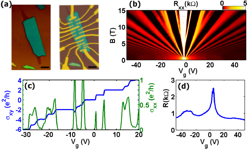
To evaluate the quality of our graphene-on-hBN devices we focus on the low- mobility and on the width of the minimum in the conductivity -vs- curve. The mobility measures the elastic scattering time responsible for momentum relaxation, whereas quantifies the potential fluctuations experienced by electrons in graphene Martin et al. (2008); Castro Neto et al. (2009). Since these potential fluctuations are not a priori the dominant source of elastic scattering, there is no reason to assume that and are related. Experimentally, the carrier mobility is obtained from (see Fig. 2(a)), with the density of charge carriers obtained through the Hall resistance. To extract we plot as a function of , and determine at which the constant value of measured at low density crosses the value of extrapolated (linearly) from high density (as shown in Fig. 2(b)). The mobility is estimated for .
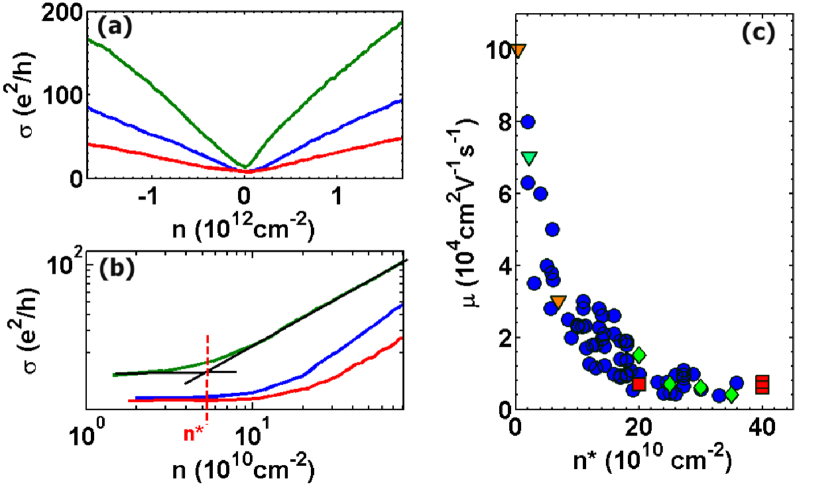
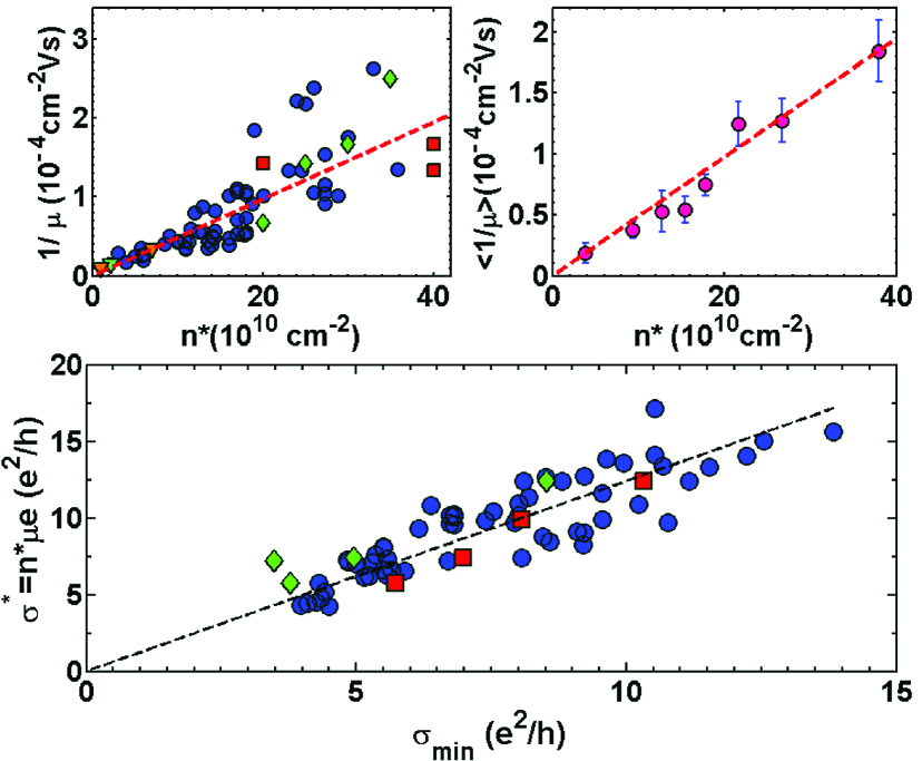
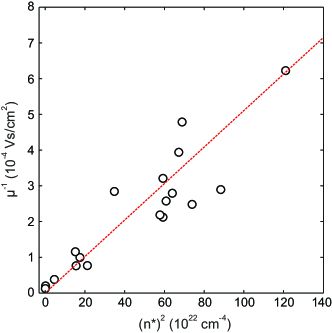
Fig. 2(c) shows as a function of for all devices, measured either immediately after fabrication, or after a subsequent annealing step. The presence of a correlation between and is unambiguous: devices with smaller density fluctuations have larger mobility. For hBN devices fabricated in our laboratory, this correlation extends from values of 5.000 cm2/Vs (for devices after multiple annealing steps, see below) to 80.000 cm2/Vs. Results reported in the literature Dean et al. (2010); Zomer et al. (2011); Dean et al. (2011) quantitatively fit the same trend, extending the range to cm2/Vs. Plotting -vs- (Fig. 3(a)) shows that the relation between these two quantities is essentially linear. To reduce the statistical fluctuations we subdivide the axis into eight different intervals and plot the inverse averaged mobility as a function of the average charge density fluctuations (Fig. 3(b)), which makes the linear scaling of with apparent.
We emphasize that neither the occurrence of the relation between and , nor its approximate linearity, are obvious a priori. Indeed, it has been shown that when intentionally creating carbon vacancies, no such relation is observed, because in that case vacancies are the dominant mechanism responsible for the suppression of the carrier mobility, but they are not the dominant mechanism causing charge inhomogeneity Chen et al. (2009). Our observations, therefore, unambiguously establish that scattering of charge carriers and charge inhomogeneity in devices on hBN are caused by the same microscopic mechanism. Also the linearity of the -vs- relation is not trivial: we have measured several graphene bilayer devices on hBN and SiO2 and found that a relation between and occurs also in that case, but the the relation is quadratic and not linear (see Appendix B). These considerations make clear that a quantitative analysis of the -vs- relation can provide important information. Note that a correlation similar to the one shown in Fig. 3(a,b) has been reported for graphene covered by ionized potassium atoms, which do generate disorder consistent with the charged impurities mechanism Chen et al. (2008a). On this basis, one may be tempted to conclude that charged impurities are also the dominant source of disorder for graphene on hBN. As we will show below, however, the -vs- correlation is also qualitatively and quantitatively compatible with the effect of random strain fluctuations in graphene, and discriminating between charged impurities and strain is the main goal of the remaining part of this paper. Before coming to that, we notice that, rather surprisingly, the -vs- correlation is fulfilled also by devices on different substrate materials, whose data point –the red and green dots in Fig. 2(c) represent data obtained from graphene on SiO2 and SrTiO3 Couto et al. (2011)– fall on the curve defined by the results obtained for graphene devices on hBN 111In Ref. Couto et al. (2011) we discussed transport through graphene-on-SrTiO3 in the context of resonant scattering, but we also pointed out –in Ref. (21) of that paper– that the data are compatible with scattering by ripples, i.e. with the conclusions of this present work..
III The characteristic scattering times reveal the origin of disorder
Having established that scattering of charge carriers and carrier density inhomogeneities are caused by the same microscopic mechanism, we can gain additional insight by analyzing weak-localization to extract all the relevant scattering times for graphene on hBN McCann et al. (2006); Morpurgo and Guinea (2006); Tikhonenko et al. (2008). Our first goal is to compare the inter-valley scattering time to the elastic scattering time determined from the carrier mobility. Either , implying that the mobility is determined by inter-valley scattering processes (i.e., the dominant source of disorder are short-range potentials), or , indicating that is limited by intra-valley scattering (i.e., long-range disorder potentials dominate). Surprisingly, this straightforward argument has not been used systematically in previous work to identify the dominant disorder, nor has it been suggested in theoretical work (for an exception, see Ref. Guignard et al. (2012) dealing with rather low mobility devices, cm2/Vs).
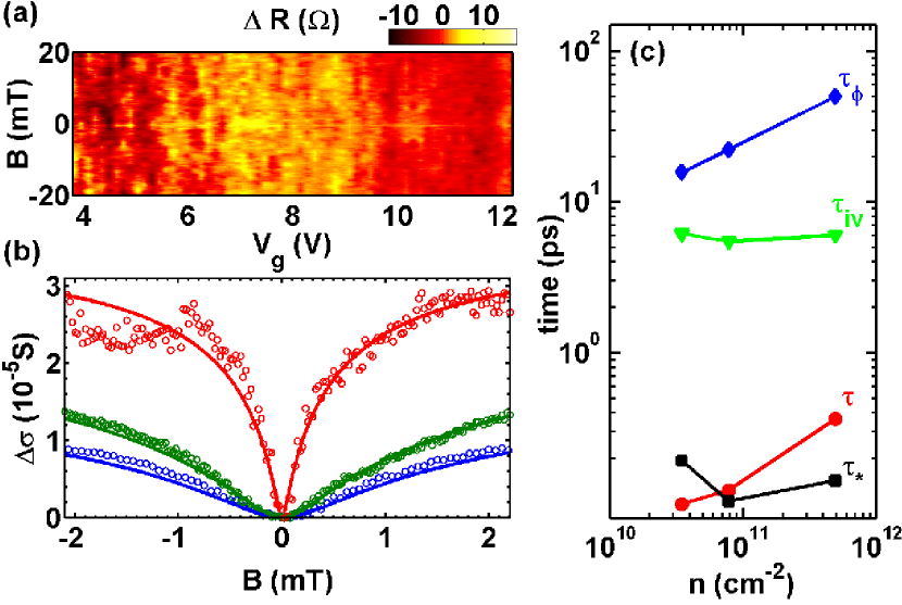
Fig. 4(a) shows the low-field magneto-resistance of a Hall bar device with cm2/Vs, for different values of around V, at mK. A narrow dip in conductivity (width mT or less) is seen around T, originating from weak localization. Aperiodic conductance fluctuations due to random interference are also visible, which we suppress by averaging measurements taken for slightly different values Ferry and Goodnick (2009). "Ensemble-averaged" curves obtained in this way around three different values are shown in Fig. 4(b). We have performed similar measurements at several different temperatures, and analyzed the ensemble-averaged low-field magneto-transport up to K.
To analyze the data, we have followed the same procedure used in previous studies of the quantum correction to the conductivity done on graphene on SiO2 substrates Tikhonenko et al. (2008); Guignard et al. (2012) and on epitaxial graphene on SiC Baker et al. (2012). Specifically, the data are fit to existing theory McCann et al. (2006), from which we extract the inter-valley scattering time , the phase coherence time , and the time needed to break effective single-valley time reversal symmetry Morpurgo and Guinea (2006), using the equation
| (1) | |||||
Here , is the digamma, function, and . In fitting the magneto-transport curves at different temperatures, we allow to vary –since the phase coherence time does increase with lowering – and we constrain the other scattering times to be constant in the range investigated (250 mK and 10 K). We obtain satisfactory agreement in all cases with a single set of value for and (the elastic scattering time –also constant as a function of – is obtained from the measurements of the conductivity, and is not a fitting parameter).
Fig. 4(c) shows the hierarchy of the relevant times at mK, the lowest temperature reached in the experiments, for three different values of . At this temperature, is much larger than , which is why weak-localization is observed ( eventually becomes shorter than as reaches 10 K, so that weak antilocalization becomes visible, in conformity to theoretical expectations, and as found previously for graphene on SiO2 Tikhonenko et al. (2008); Guignard et al. (2012)). More importantly throughout the density range investigated by at least one order of magnitude, (and by nearly two at low ). This last observation implies that intra-valley scattering is the process limiting , a result that –in conjunction with previous measurements on graphene-on-SiO2 Tikhonenko et al. (2008); Guignard et al. (2012)– holds at least in the mobility range between 1.000 and 80.000 cm2/Vs. We conclude that weak-localization measurements unambiguously show that the dominant source of disorder for exfoliated mono-layer graphene on hBN (and SiO2) substrates is associated to long-ranged potentials (motivated by this conclusion, we have also recently studied weak-localization on high-quality graphene bilayer devices on hBN substrates, and in that case as well we have unambiguously come to the same conclusion, namely that it is intra-valley scattering processes that are limiting the carrier mobility Engels et al. (2014)).
The results of the weak-localization measurements also provide a clear indication as to which of the two sources of long-range disorder (charged impurities at the substrate surface Adam et al. (2007); Ando (2006); Nomura and MacDonald (2007) and random strain fluctuations in the graphene lattice Katsnelson and Geim (2008)) plays the most relevant role. Specifically, the analysis of weak-localization shows that within a factor of 2-3, for all carrier density range investigated (Fig. 4(b)), a finding that is naturally explained by strain. Indeed, strain generates random pseudo-magnetic fields Vozmediano et al. (2010) that not only scatter charge carriers, but also break the effective time reversal symmetry in a single-valley Morpurgo and Guinea (2006); McCann et al. (2006) on approximately the same time scale. If these random pseudo-magnetic fields are the dominant source of scattering limiting the mobility, we can immediately understand why and are comparable. On the contrary, for a potential generated by charged impurities on and in the substrate, is determined by the Fourier components with , whereas is determined by random fluctuations in the potential difference between the A and B atoms in the individual unit cells of graphene, i.e. by the Fourier component of with (see Appendix C). Since is a long-range potential, , implying (through Fermi golden rule) that for charged impurities , in disagreement with the experimental observations. We are not aware of any mechanism other than strain-induced pseudo-magnetic fields that can explain the coincidence between and , which is why the indication of this finding for the relevance of local strain fluctuations is rather compelling.
Albeit less directly, the experimentally observed evolution of upon annealing also points to the effect of strain. As discussed above, repeated annealing at low temperature ( ∘C) in an inert atmosphere systematically reduces by one order of magnitude. These annealing processes have no significant chemical effect, and therefore are not expected to change the density of charge at the surface of hBN by one order of magnitude (as it would be needed to explain the changes in Adam et al. (2007)). On the contrary, they do lead to visible mechanical deformations, compatible with strain causing a decrease in mobility. Finally, having limited by strain-induced pseudo-magnetic fields also explains why the use of high- substrates –such as SrTiO3 Couto et al. (2011)– does not lead to a very large increase in mobility: a high- substrate can screen scalar potentials, but not the effect of a pseudo-magnetic field.
IV Raman mapping for correlating strain fluctuations and carrier mobility
Additional indications that carrier mobility in graphene is limited by local strain fluctuations can be obtained by combining transport measurements with spatially resolved Raman spectroscopy Graf et al. (2007); Lee et al. (2012). The quantity of interest in this case is the line-width of the Raman 2D-peak, . In contrast to the width of the G-peak, does only very weakly depend on doping, charge inhomogeneities Pisana et al. (2007); Stampfer et al. (2007); Berciaud et al. (2013), or magnetic field Neumann et al. (2014). is also only weakly affected by global strain and by the different screening properties of the substrates Popov and Lambin (2013); Forster et al. (2013), while it is highly sensitive to strain inhomogeneities on length-scales smaller the laser-spot size ( nm), as recently shown by Neumann and coworkers Neumann et al. (2014). These are precisely the random strain fluctuations that can contribute to scattering of charge carriers.
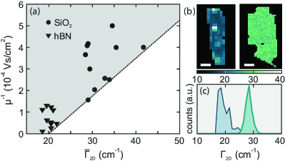
Fig. 5(a) shows the inverse mobility versus the line-width of the 2D-peak for a number of contacted graphene flakes resting on different substrates. Each of the data points corresponds to a different sample, on which we performed low-temperature (=1.8 K) transport measurements to extract the mobility , as well as spatially resolved Raman maps, such as those of Fig. 5(b) (the color code represents the line-width of the local 2D-peak). From these maps we extract for each flake the distribution of , see Fig. 5(c), from which we calculate the average width (this is the quantity plotted on the horizontal axis of Fig. 5(a)). Values of larger than the intrinsic line-width of the 2D-peak are indicative of strain fluctuations in the graphene layer Neumann et al. (2014), and a larger corresponds to a larger magnitude of these random strain fluctuations.
Finding that the data points from all the investigated devices in Fig. 5(a) lie above the dotted lines means that the maximum observed value of is smaller in devices for which is larger, i.e., in devices with larger random strain fluctuations. This directly indicates that strain is limiting the carrier mobility. The data show a rather large spread in mobility values, which originates from the fact that the mobility can be limited by structural defects –like folds formed in graphene during the transfer and fabrication process– which can have only a small effect on the averaged linewidth . Indeed, the devices used for these combined Raman and transport measurements were not etched to confine transport through regions in which these types of structural defects are absent, since etching would have drastically reduced the area of graphene, making Raman measurements considerably more complex. As a result, a quasi one-dimensional fold or ripple cutting across the graphene flake (see e.g. white regions in Fig. 5(b), left panel) can have a very strong effect on the mobility value extracted in the device, while –as it affects only a small part of the total device area– it has only a small effect on the averaged linewidth . Despite these experimental limitations, the absence of data points in the non-shaded area indicates that a necessary condition to observe high carrier mobility values is to have small random strain fluctuations, and the correlation between maximum mobility and averaged linewidth is clearly apparent in the data.
V Quantitative explanation of the -vs- correlation in terms of strain
Having found a direct correlation between the strength of the random local strain in graphene and the carrier mobility –and therefore having confirmed the role of strain fluctuations as an important source of disorder– we check, for consistency, whether the relation between and that we discussed earlier (see Fig. 3(a,b)) can be explained theoretically in terms of strain fluctuations only. As we mentioned already, such a relation has been reported experimentally earlier on, in the study of transport through graphene exposed to an increasingly large density of potassium atoms, where it was naturally explained in terms of the effect of charged impurities (the ionized potassium atoms) Chen et al. (2008a). Here below we show that the relation between and is very naturally reproduced also if random local strain is the dominant source of disorder. Indeed, at the quantitative level, the experimental data agree with theoretical calculations for realistic values (i.e., in the range known from literature) of the elastic parameters of graphene, which describe the coupling between strain and electronic properties.
Strain can originate from both in-plane and out-of-plane deformations (the latter being the so-called ripples), with the former being probably the most relevant ones, especially on hBN substrates. The effect of random strain fluctuations on the motion of electrons in graphene can be described by introducing a scalar and a vector potential and in the long-wavelength Dirac Hamiltonian. What is needed to calculate the effect of strain fluctuations on and are the correlation functions of these potentials, which can all be obtained directly from the correlation function of the random strain field (as described in Appendix A). The scalar and the gauge potential scatter electrons (with rates and , respectively) and limit the mobility . The magnitude of the charge fluctuations , on the contrary, is determined by the scalar potential only. We calculate and using Fermi golden rule, and obtain the total scattering time as :
| (2) |
and
| (3) |
where is the component of perpendicular to , is the one-valley density of states at the Fermi energy, is the dielectric function including the substrate contribution, and , , and are the Fermi momentum, velocity, and energy. We extract the mobility from (the factor of 2 accounts for the two valleys). To calculate the magnitude of charge fluctuations we use the relation between local charge density and potential, from which:
| (4) |
Since the correlation functions of all the potentials are determined by the same correlation function describing the random strain field, and are related. We find in all cases a linear relation between and (within logarithmic corrections) with a slope determined by the elastic coefficients of graphene, whose specific expression differs for out-of-plane and for in-plane strain. For out-of-plane strain we have
| (5) |
whereas for in-plane strain we obtain
| (6) |
In both expressions, the first term in the square bracket originates from the contribution to scattering of the scalar potential and the second from that of the pseudo-magnetic field. In these expressions, and quantify the strength of electron-phonon coupling in graphene, eV/Å2 and eV/Å2 are Lamé coefficients Zakharchenko et al. (2009), and ( is the lattice constant of graphene and the logarithm appears when cutting off the integrals at large -values, at ). Eqs. (5) and (6) show that the relation between and is linear (the deviations caused by the logarithm are within the fluctuations in the data, and in fact improve the overall agreement) as found experimentally. Notably, these relations only depend on fundamental constants and on the elastic properties of graphene. In this regard, the only role of the substrate is to determine the magnitude of the strain present in the graphene lattice.
The dashed lines in Fig. 3(a),(b) are best fits to the data (). Both expressions above for random out-of-plane or in-plane strain reproduce this value of the slope with realistic values of the and parameters (the slope only depends on their ratio). The parameter is determined by the modulation of the hopping between orbitals and the strain, and it can be extracted from measurements of effective magnetic fields created in highly strained graphene Levy et al. (2010). A reasonable value is eV Gibertini et al. (2012). The parameter gives the strength of the scalar potential, and estimates of its magnitude vary in the range eV Ono and Sugihara (1966); Suzuura and Ando (2002); Choi et al. (2010); Gibertini et al. (2012). Using and fixing eV, the expression for random strain due to ripples Eq.(5) reproduces the slope of the -vs- for eV, and if Eq. (6) for in-plane strain is taken, the experimental value is obtained for eV, in all cases fully compatible with the expected range of values. We conclude that random strain quantitatively accounts for the -vs- relation observed in the experiments. While both in-plane or out-of-plane random strain contribute, it is likely that on hBN substrates in-plane strain dominates.
Having fixed the values of by comparing the theoretical expression for with the experimental data, we can determine whether it is the scalar or the gauge potential originating from strain that gives the dominant contribution to the scattering time. Interestingly we find that for both out-of-plane and in-plane random strain, the scattering time associated to the random gauge potential is approximately one order of magnitude smaller than the scattering time associated to the scalar potential , i.e. it is the gauge potential that poses the most stringent limit to the mobility. This is exactly what we would expect from our analysis of weak-localization, and specifically from the experimental observation that . This finding also explains why the use of high dielectric constant substrates (such as SrTiO3) cannot lead to a major increase in mobility Couto et al. (2011): a high- substrate could screen the deformation potential –which is electrostatic in nature– but not the effect of a random pseudo-magnetic field. We conclude that our theoretical analysis of the -vs- relation does not only reproduce the experimental data with realistic values of the model parameters, but it is also internally consistent with other independent experimental observations. It is this level of quantitative agreement and internal consistency of results obtained by means of different techniques that strongly supports the validity of our interpretation.
VI Conclusions
The experimental and theoretical results discussed above lead to a consistent physical scenario which can be understood only if random strain fluctuations are the dominant source of disorder in graphene on hBN (and other) substrates. We summarize the key points. The analysis of weak-localization measurements shows that , implying that scattering of charge carriers occurs mainly within the same valley, and that is therefore due to a long-range potential. It also shows that the characteristic time to break the effective single-valley time reversal symmetry is comparable to , the elastic scattering time extracted from the mobility, a finding that can be explained naturally if random pseudo-magnetic fields due to strain are the dominant scattering mechanism. Since this finding () does not appear to be compatible with any other disorder mechanism, the indication that it provides as to the relevance of random strain fluctuations is particularly compelling. The role of local strain fluctuations is further confirmed by the correlation between the maximum observed mobility with the line width of the Raman 2D-peak measured on the very same devices (which has been identified as a measure of the intensity of local mechanical deformations, i.e. local strain). Finally, a conceptually straightforward theoretical analysis shows that strain provides a qualitative and quantitative understanding of the linear relation between and . This same analysis confirms that strain-induced disorder mainly generates scattering through random pseudo-magnetic fields, and not through the scalar deformation potential, which is precisely what we had concluded independently through the study of weak localization.
Although most considerations above have been made for graphene on hBN, our results point to the relevance of strain fluctuation also for graphene on SiO2 and SrTiO3 substrates. Indeed, data obtained from devices on SiO2 and SrTiO3 satisfy quantitatively the same -vs- relation that we have found analyzing many devices on hBN. For graphene on SiO2, weak-localization measurements done in the past Tikhonenko et al. (2008); Guignard et al. (2012) allow us to draw conclusions similar to those that we have discussed here for devices on hBN. Additionally, random strain fluctuations explain why devices made on substrates with extremely different surface chemistry show similar mobility ( cm2/Vs), a fact that would be difficult to understand if charge impurities at the substrate surface were the dominating source of disorder (simply because the density of charged impurities should depend very strongly on the specific chemical groups present at the substrate surface). Finally, the finding that strain fluctuations dominantly couples to the electrons through the generation of a random pseudo-magnetic field –and not through the deformation potential– explains why the mobility in devices on SrTiO3 substrates Couto et al. (2011), which have a very high dielectric constant, is not much higher than on SiO2, since the effect of magnetic field cannot be screened electrostatically.
VII Acknowledgements
AFM gratefully acknowledges support by the SNF and by the NCCR QSIT. FG acknowledges support from the Spanish Ministry of Economy (MINECO) through Grant No. FIS2011-23713 and the European Research Council Advanced Grant (contract 290846). CS and SE acknowledge experimental help from F. Buckstegge, J. Dauber, B. Terrés, F. Vollmer and M. Drögeler and financial support from DFG and ERC (contract 280140). AFM, FG and CS acknowledge funding from the EU under the Graphene Flagship.
VIII Appendix A: Analysis of strain distributions.
We discuss the technical details of the analysis of the effects of random strain, and derive the expressions for the relations between and reported in the main text. Strains can be induced either by out-of-plane corrugations, or by in-plane displacements of the atoms in the graphene lattice. We analyze the two cases separately. We emphasize that this same analysis is consistent with the observed density dependence of the mobility: irrespective of whether strain is in-plane or out-of-plane, the calculated mobility is independent of carrier density, within logarithmic corrections that cause a slow mobility suppression at large .
VIII.1 Out of plane corrugations.
We assume a given height profile, . The height corrugations lead to strains, which induce a scalar and a gauge potential acting on the electrons Vozmediano et al. (2010):
| (7) |
where and are parameters with dimensions of energy, and are the elastic Lamé coefficients. , with the Fourier transform of , , with , and Zakharchenko et al. (2009).
We assume that the height correlations are such that
| (8) |
where is a constant. This dependence corresponds to the profile of a membrane with temperature , where is the bending rigidity of graphene Katsnelson and Geim (2008). This assumption leads to , where is a dimensionless constant. It is given, approximately, by
| (9) |
where and are typical values for the height and size of the ripples. Using eqs. (2) and (3), we find
| (12) | ||||
| (13) |
The mobility is given by .
For , the mobility is
| (14) |
The scalar potential in eq.(7) gives rise to charge fluctuations, whose amplitude is given by:
| (15) |
The ratio of the two expressions above leads to the -vs- relation, Eq. (5) in the main text.
VIII.2 In plane strains.
A supporting substrate induces forces on the carbon atoms of a graphene layer, leading to strains and deformations. Therefore, next to out of plane deformations (discussed in the previous section) that can occur on a corrugated substrate, or because of imperfect adhesion during the graphene transfer process, in plane forces on the Carbon atoms can also be expected. These forces induce strains, which modify the electronic properties. In particular, periodic interactions, associated to the incommensuration between the lattices of graphene and the substrate, lead to the formation of superstructures and Moiré patterns Woods et al. (2014); Jung et al. (2014); San-Jose et al. (2014). In addition, a random distribution of forces should be expected, due to impurities in the substrates, and other imperfections in the graphene/substrate system (e.g., remnants of adsorbates in between the substarte and graphene).
We neglect the short range, periodic component of the interaction potential between graphene and the substrate, and consider a random potential, , which varies slowly over a distance , where is the lattice constant
| (16) |
This potential leads to forces at the positions of the carbon atoms
| (17) |
The elastic energy of the graphene lattice is
| (18) |
where is the area of the unit cell, is the lattice constant, is the displacement of the atom at position from its equilibrium position, , and we assume that the displacements are small, so that the assumption of a linear coupling to local forces is valid.
We Fourier transform eq. (18)
| (19) |
For long wavelength force distributions, , where is a reciprocal vector of the graphene lattice, the displacements are
| (20) |
where the and superscripts stand for the parallel and transverse components of with respect to (, the vector has only a longitudinal component, but this is not the generic case, see below.). If , long wavelength displacements are also generated
| (21) |
where now the superscripts and refer to the orientation of with respect to . From we can obtain the strain tensor
| (22) |
For we have , while for we obtain . Thus, we obtain two different contributions to the correlations of long range strains
| (23) |
where . In the following we will concentrate on the effects of the random components of the potential of order . The contribution to the transport properties is larger that that from small momenta by terms of order .
The scalar and gauge potentials are
| (24) |
The gauge potential can be divided into a component , parallel to , and a component , perpendicular to . The effect of can be gauged away, and only gives a physical effect. In terms of the potential correlations we find
| (25) |
where is the angle between and , is the area of the unit cell of the graphene lattice, and we neglect terms proportional to quantities like which average to zero when summing over . The factor arises from extracting the component of normal to .
APPENDIX B: 1/-vs- RELATION FOR BILAYER GRAPHENE
Here, we illustrate that the linearity of the relation between and for monolayer graphene is not trivial, by comparing the result shown in Fig. 3 to those of a similar analysis done for bilayer graphene devices (the bilayer devices have been fabricated on hBN and SiO2 substrates, following protocols identical to those used for the monolayers). The result is illustrated in Fig. 6, in which we plot as a function of : it is apparent that the experimental data obey a linear relation, i.e., for bilayers , in contrast to the relation found in monolayers. This finding further supports our theoretical analysis of disorder in monolayers in terms of strain, which correctly captures the observed, non-trivial linear dependence of the relation between and .
IX Appendix C: Weak-Localization and single-valley effective time reversal symmetry
Weak-localization measurements in graphene provide a wealth of information about the scattering processes that take place in the material. As we have discussed in the main text, we can conclude directly from the results of the fits of the magneto-resistance curves that the intervalley scattering time is much longer than the elastic scattering time , which indicates that intra-valley scattering processes –and therefore long-range potentials– dominate the effect of disorder. We have also found that the elastic scattering time nearly coincides with the time needed to break the effective single-valley time reversal symmetry, and argued that this observation strongly indicates that strain –and not charged impurities– is the dominant scattering source. As the reader may not be fully familiar with the concept of effective single-valley time reversal symmetry, we discuss this here in some more detail for completeness (for more information, see Ref. Morpurgo and Guinea (2006)).
Effective single-valley time reversal symmetry is a concept relevant for graphene, in the regime in which a continuum Dirac Hamiltonian provides a good description (i.e., when the Fermi level is not too far away from the charge neutrality point). In the ideal case, the Dirac Hamiltonian (where is the momentum relative to the K-point)
| (29) |
is invariant upon the anti-unitary transformation , with denoting complex conjugation. This anti-unitary transformation mimics the implementation of time-reversal symmetry, as –for each electronic state– it sends into and reverses the spin. However, this is not the true time reversal symmetry operation. Indeed, true time reversal symmetry changes the sign of the total momentum (and not just of the momentum relative to the K point) and sends states in one of the valley into the other valley (time reversal symmetry therefore cannot be implemented by considering one valley only). That is why is referred to as "effective single-valley time reversal symmetry". While it remains a good symmetry as long as is well approximated by the Dirac Hamiltonian, the implication of not being the "true" time reversal operation is that it can be easily violated, by different microscopic mechanisms.
For instance, effective time reversal symmetry is violated by the quadratic momentum terms that are neglected when making the linear approximation in the continuum, which leads to the Dirac Hamiltonian. It is obvious that –being quadratic– these terms do not change sign upon inverting the sign of , whereas the linear terms in the Dirac Hamiltonian do. As a result, when including both the linear and quadratic terms in , the single-valley Hamiltonian is not invariant upon effective single-valley time reversal symmetry. This mechanism, however, cannot account for our experimental observations ( independent of carrier density): the effect of the quadratic terms become more relevant as is increased further away from the charge neutrality point. If these terms were the relevant ones in determining the characteristic time scale , we should find that becomes shorter at larger carrier density, contrary to what we observe experimentally (see Fig. 4c of the main text). Additionally, this mechanism cannot explain why , because the quadratic terms in do not cause any scattering of electron waves.
Other two mechanisms that break effective time reversal symmetry are strain, and the presence of a "gap" term in the Dirac Hamiltonian. Strain breaks the effective time reversal symmetry by generating a random pseudo-magnetic field. Indeed, within a single valley, this pseudo magnetic field acts on the orbital degrees of freedom in all regards as a true magnetic field, i.e., it is described by a gauge potential minimally coupled to the momentum. If the dominant source of scattering are spatial inhomogeneities in this gauge potential, such a mechanism very naturally explains why the elastic scattering time and the time needed to break the effective time reversal symmetry nearly coincide, as scattering and effective time reversal symmetry breaking originate from the same term in the Hamiltonian.
A "gap" term –i.e., a difference in on-site energy between the A and B carbon atom in the unit cell of graphene– also breaks the effective single-valley time reversal symmetry. In that case the Hamiltonian becomes
| (30) |
The fact that this Hamiltonian is not invariant upon can be checked by a direct calculation. It is also obvious without doing any calculation, if we observe that this Hamiltonian is formally identical to that of Rashba spin-orbit interaction in the presence of a Zeeman term (with corresponding to /2), a system which lacks time reversal symmetry.
In our experimental case, charged impurities on a substrate can contribute to the breaking of effective time reversal symmetry through this mechanism. More specifically, charge impurities would generate random electrostatic potentials. On average, these potentials would be the same on the A and B atoms forming graphene. Nevertheless, fluctuations would exist so that locally the electrostatic on-site energy would be slightly different on the A and B atom in each unit cell, i.e., locally a non-zero term would be present. However, in our experiments, this mechanism cannot explain why the scattering time and the characteristic time for breaking effective time reversal symmetry would coincide. In fact, as discussed in the main text, this mechanism would predict that , because is determined by the Fourier components of the potential at , whereas is determined by the components at (with a long ranged potential the latter are much smaller).
Références
- Dean et al. (2010) C. R. Dean, A. F. Young, I. Meric, C. Lee, L. Wang, S. Sorgenfrei, K. Watanabe, T. Taniguchi, P. Kim, K. L. Shepard, and J. Hone, Boron nitride substrates for high-quality graphene electronics, Nat. Nano. 5, 722–726 (2010).
- Zomer et al. (2011) P. J. Zomer, S. P. Dash, N. Tombros, and B. J. van Wees, A transfer technique for high mobility graphene devices on commercially available hexagonal boron nitride, Appl. Phys. Lett. 99, 232104 (2011).
- Mayorov et al. (2011) A. S. Mayorov, R. V. Gorbachev, S. V. Morozov, L. Britnell, R. Jalil, L. A. Ponomarenko, P. Blake, K. S. Novoselov, K. Watanabe, T. Taniguchi, and A. K. Geim, Micrometer-scale ballistic transport in encapsulated graphene at room temperature, Nano Lett. 11, 2396–2399 (2011).
- Wang et al. (2013) L. Wang, I. Meric, P. Y. Huang, Q. Gao, Y. Gao, H. Tran, T. Taniguchi, K. Watanabe, L. M. Campos, D. A. Muller, J. Guo, P. Kim, J. Hone, K. L. Shepard, and C. R. Dean, One-dimensional electrical contact to a two-dimensional material, Science 342, 614–617 (2013).
- Dean et al. (2011) C. R. Dean, A. F. Young, P. Cadden-Zimansky, L. Wang, H. Ren, K. Watanabe, T. Taniguchi, P. Kim, J. Hone, and K. L. Shepard, Multicomponent fractional quantum hall effect in graphene, Nat. Phys. 7, 693–696 (2011).
- Young et al. (2012) A. F. Young, C. R. Dean, L. Wang, H. Ren, P. Cadden-Zimansky, K. Watanabe, T. Taniguchi, J. Hone, K. L. Shepard, and P. Kim, Spin and valley quantum hall ferromagnetism in graphene, Nat. Phys. 8, 550–556 (2012).
- Ponomarenko et al. (2013) L. A. Ponomarenko, R. V. Gorbachev, G. L. Yu, D. C. Elias, R. Jalil, A. A. Patel, A. Mishchenko, A. S. Mayorov, C. R. Woods, J. R. Wallbank, M. Mucha-Kruczynski, B. A. Piot, M. Potemski, I. V. Grigorieva, K. S. Novoselov, F. Guinea, V. I. Fal’ko, and A. K. Geim, Cloning of dirac fermions in graphene superlattices, Nature 497, 594–597 (2013).
- Dean et al. (2013) C. R. Dean, L. Wang, P. Maher, C. Forsythe, F. Ghahari, Y. Gao, J. Katoch, M. Ishigami, P. Moon, M. Koshino, T. Taniguchi, K. Watanabe, K. L. Shepard, J. Hone, and P. Kim, Hofstadter’s butterfly and the fractal quantum hall effect in moire superlattices, Nature 497, 598–602 (2013).
- Hunt et al. (2013) B. Hunt, J. D. Sanchez-Yamagishi, A. F. Young, M. Yankowitz, B. J. LeRoy, K. Watanabe, T. Taniguchi, P. Moon, M. Koshino, P. Jarillo-Herrero, and R. C. Ashoori, Massive dirac fermions and hofstadter butterfly in a van der waals heterostructure, Science 340, 1427–1430 (2013).
- Castro Neto et al. (2009) A. H. Castro Neto, F. Guinea, N. M. R. Peres, K. S. Novoselov, and A. K. Geim, The electronic properties of graphene, Rev. Mod. Phys. 81, 109 (2009).
- Chen et al. (2008a) J. H. Chen, C. Jang, S. Adam, M. S. Fuhrer, E. D. Williams, and M. Ishigami, Charged-impurity scattering in graphene, Nat. Phys. 4, 377–381 (2008a).
- Chen et al. (2009) J.-H. Chen, W. G. Cullen, C. Jang, M. S. Fuhrer, and E. D. Williams, Defect scattering in graphene, Phys. Rev. Lett. 102, 236805 (2009).
- Adam et al. (2007) S. Adam, E. H. Hwang, V. M. Galitski, and S. Das Sarma, A self-consistent theory for graphene transport, Proc. Natl. Acad. Sci. USA 104, 18392 (2007).
- Jang et al. (2008) C. Jang, S. Adam, J.-H. Chen, E. D. Williams, S. Das Sarma, and M. S. Fuhrer, Tuning the effective fine structure constant in graphene: Opposing effects of dielectric screening on short- and long-range potential scattering, Phys. Rev. Lett. 101, 146805 (2008).
- Ponomarenko et al. (2009) L. A. Ponomarenko, R. Yang, T. M. Mohiuddin, M. I. Katsnelson, K. S. Novoselov, S. V. Morozov, A. A. Zhukov, F. Schedin, E. W. Hill, and A. K. Geim, Effect of a high- environment on charge carrier mobility in graphene, Phys. Rev. Lett. 102, 206603 (2009).
- Peres (2010) N. M. R. Peres, Colloquium: The transport properties of graphene: An introduction, Rev. Mod. Phys. 82, 2673 (2010).
- Monteverde et al. (2010) M. Monteverde, C. Ojeda-Aristizabal, R. Weil, K. Bennaceur, M. Ferrier, S. Guéron, C. Glattli, H. Bouchiat, J. N. Fuchs, and D. L. Maslov, Transport and elastic scattering times as probes of the nature of impurity scattering in single-layer and bilayer graphene, Phys. Rev. Lett. 104, 126801 (2010).
- Das Sarma et al. (2011) S. Das Sarma, S. Adam, E. H. Hwang, and E. Rossi, Electronic transport in two-dimensional graphene, Rev. Mod. Phys. 83, 407 (2011).
- Couto et al. (2011) N. J. G. Couto, B. Sacepe, and A. F. Morpurgo, Transport through graphene on srtio3, Phys. Rev. Lett. 107, 225501 (2011).
- Adam et al. (2011) S. Adam, S. Jung, N. N. Klimov, N. B. Zhitenev, J. A. Stroscio, and M. D. Stiles, Mechanism for puddle formation in graphene, Phys. Rev. B 84, 235421 (2011).
- Neumann et al. (2014) C. Neumann, S. Reichardt, M. Drogeler, K. Watanabe, T. Taniguchi, B. Beschoten, S. V. Rotkin, and C. Stampfer, Magneto-raman microscopy for probing local material properties of graphene, ArXiv e-prints (2014), arXiv:1406.7771 [cond-mat.mes-hall] .
- Taychatanapat et al. (2013) T. Taychatanapat, K. Watanabe, T. Taniguchi, and P. Jarillo-Herrero, Electrically tunable transverse magnetic focusing in graphene, Nat. Phys. 9, 225–229 (2013).
- Chen et al. (2008b) J.-H. Chen, C. Jang, S. Xiao, M. Ishigami, and M. S. Fuhrer, Intrinsic and extrinsic performance limits of graphene devices on sio2, Nat. Nano. 3, 206–209 (2008b).
- Martin et al. (2008) J. Martin, N. Akerman, G. Ulbricht, T. Lohmann, J. H. Smet, K. von Klitzing, and A. Yacoby, Observation of electron-hole puddles in graphene using a scanning single-electron transistor, Nat. Phys. 4, 144–148 (2008).
- Note (1) In Ref. Couto et al. (2011) we discussed transport through graphene-on-SrTiO3 in the context of resonant scattering, but we also pointed out –in Ref. (21) of that paper– that the data are compatible with scattering by ripples, i.e. with the conclusions of this present work.
- McCann et al. (2006) E. McCann, K. Kechedzhi, Vladimir I. Fal’ko, H. Suzuura, T. Ando, and B. L. Altshuler, Weak-localization magnetoresistance and valley symmetry in graphene, Phys. Rev. Lett. 97, 146805 (2006).
- Morpurgo and Guinea (2006) A. F. Morpurgo and F. Guinea, Intervalley scattering, long-range disorder, and effective time-reversal symmetry breaking in graphene, Phys. Rev. Lett. 97, 196804 (2006).
- Tikhonenko et al. (2008) F. V. Tikhonenko, D. W. Horsell, R. V. Gorbachev, and A. K. Savchenko, Weak localization in graphene flakes, Phys. Rev. Lett. 100, 056802 (2008).
- Guignard et al. (2012) J. Guignard, D. Leprat, D. C. Glattli, F. Schopfer, and W. Poirier, Quantum hall effect in exfoliated graphene affected by charged impurities: Metrological measurements, Phys. Rev. B 85, 165420– (2012).
- Ferry and Goodnick (2009) D. K. Ferry and S. M. Goodnick, Transport in Nanostructures (Cambridge University Press, 2009).
- Baker et al. (2012) A. M. R. Baker, J. A. Alexander-Webber, T. Altebaeumer, T. J. B. M. Janssen, A. Tzalenchuk, S. Lara-Avila, S. Kubatkin, R. Yakimova, C.-T. Lin, L.-J. Li, and R. J. Nicholas, Weak localization scattering lengths in epitaxial, and cvd graphene, Phys. Rev. B 86, 235441 (2012).
- Engels et al. (2014) S. Engels, B. Terrés, A. Epping, T. Khodkov, K. Watanabe, T. Taniguchi, B. Beschoten, and C. Stampfer, Limitations to carrier mobility and phase-coherent transport in bilayer graphene, ArXiv e-prints (2014), arXiv:1403.1547 [cond-mat.mes-hall] .
- Ando (2006) T. Ando, Screening effect and impurity scattering in monolayer graphene, J. Phys. Soc. Jpn. 75, 074716 (2006).
- Nomura and MacDonald (2007) K. Nomura and A. H. MacDonald, Quantum transport of massless dirac fermions, Phys. Rev. Lett. 98, 076602 (2007).
- Katsnelson and Geim (2008) M. I. Katsnelson and A. K. Geim, Electron scattering on microscopic corrugations in graphene, Phil. Trans. R. Soc. A 366, 195–204 (2008).
- Vozmediano et al. (2010) M. A. H. Vozmediano, M. I. Katsnelson, and F. Guinea, Gauge fields in graphene, Phys. Rep. 496, 109–148 (2010).
- Graf et al. (2007) D. Graf, F. Molitor, K. Ensslin, C. Stampfer, A. Jungen, C. Hierold, and L. Wirtz, Spatially resolved raman spectroscopy of single- and few-layer graphene, Nano Lett. 7, 238–242 (2007).
- Lee et al. (2012) J. E. Lee, G. Ahn, J. Shim, Y. S. Lee, and S. Ryu, Optical separation of mechanical strain from charge doping in graphene, Nat. Commun. 3, 1024 (2012).
- Pisana et al. (2007) S. Pisana, M. Lazzeri, C. Casiraghi, K. S. Novoselov, A. K. Geim, A. C. Ferrari, and F. Mauri, Breakdown of the adiabatic born-oppenheimer approximation in graphene, Nat. Mater. 6, 198–201 (2007).
- Stampfer et al. (2007) C. Stampfer, F. Molitor, D. Graf, K. Ensslin, A. Jungen, C. Hierold, and L. Wirtz, Raman imaging of doping domains in graphene on sio2, Appl. Phys. Lett. 91, 241907 (2007).
- Berciaud et al. (2013) S. Berciaud, X. Li, H. Htoon, L. E. Brus, S. K. Doorn, and T. F. Heinz, Intrinsic line shape of the raman 2d-mode in freestanding graphene monolayers, Nano Lett. 13, 3517–3523 (2013).
- Popov and Lambin (2013) V. N. Popov and P. Lambin, Theoretical 2d raman band of strained graphene, Phys. Rev. B 87, 155425 (2013).
- Forster et al. (2013) F. Forster, A. Molina-Sanchez, S. Engels, A. Epping, K. Watanabe, T. Taniguchi, L. Wirtz, and C. Stampfer, Dielectric screening of the kohn anomaly of graphene on hexagonal boron nitride, Phys. Rev. B 88, 085419 (2013).
- Zakharchenko et al. (2009) K. V. Zakharchenko, M. I. Katsnelson, and A. Fasolino, Finite temperature lattice properties of graphene beyond the quasiharmonic approximation, Phys. Rev. Lett. 102, 046808– (2009).
- Levy et al. (2010) N. Levy, S. A. Burke, K. L. Meaker, M. Panlasigui, A. Zettl, F. Guinea, A. H. Castro Neto, and M. F. Crommie, Strain-induced pseudo-magnetic fields greater than 300 tesla in graphene nanobubbles, Science 329, 544–547 (2010).
- Gibertini et al. (2012) M. Gibertini, A. Tomadin, F. Guinea, M. I. Katsnelson, and M. Polini, Electron-hole puddles in the absence of charged impurities, Phys. Rev. B 85, 201405 (2012).
- Ono and Sugihara (1966) S. Ono and K. Sugihara, Theory of the transport properties in graphite, J. Phys. Soc. Jpn. 21, 861–868 (1966).
- Suzuura and Ando (2002) H. Suzuura and T. Ando, Phonons and electron-phonon scattering in carbon nanotubes, Phys. Rev. B 65, 235412 (2002).
- Choi et al. (2010) S.-M. Choi, S.-H. Jhi, and Y.-W. Son, Effects of strain on electronic properties of graphene, Phys. Rev. B 81, 081407 (2010).
- Woods et al. (2014) C. R. Woods, L. Britnell, A. Eckmann, R. S. Ma, J. C. Lu, H. M. Guo, X. Lin, G. L. Yu, Y. Cao, R. V. Gorbachev, A. V. Kretinin, J. Park, L. A. Ponomarenko, M. I. Katsnelson, Yu N. Gornostyrev, K. Watanabe, T. Taniguchi, C. Casiraghi, H. J. Gao, A. K. Geim, and K. S. Novoselov, Commensurate-incommensurate transition in graphene on hexagonal boron nitride, Nat. Phys. 10, 451–456 (2014).
- Jung et al. (2014) J. Jung, A. DaSilva, S. Adam, and A. H. MacDonald, Origin of band gaps in graphene on hexagonal boron nitride, ArXiv e-prints (2014), arXiv:1403.0496 [cond-mat.mes-hall] .
- San-Jose et al. (2014) P. San-Jose, A. Gutiérrez-Rubio, M. Sturla, and F. Guinea, Spontaneous strains and gap in graphene on boron nitride, Phys. Rev. B 90, 075428 (2014).