Disclaimer: This work has been published in IEEE Transactions on Ultrasonics, Ferroelectrics, and Frequency Control Vol. 61, No. 7, pp 1063-1074, July 2014.
http://dx.doi.org/10.1109/TUFFC.2014.3007
Copyright with IEEE. Personal use of this material is permitted. However, permission to reprint/republish this material for advertising or promotional purposes or for creating new collective works for resale or redistribution to servers or lists, or to reuse any copyrighted component of this work in other works must be obtained from the IEEE. This material is presented to ensure timely dissemination of scholarly and technical work. Copyright and all rights therein are retained by authors or by other copyright holders. All persons copying this information are expected to adhere to the terms and constraints invoked by each author’s copyright. In most cases, these works may not be reposted without the explicit permission of the copyright holder. For more details, see the IEEE Copyright Policy
Determination of Doping and Temperature Dependent Elastic Constants of Degenerately Doped Silicon from MEMS Resonators
Abstract
Elastic constants , and of degenerately doped silicon are studied experimentally as a function of the doping level and temperature. First and second order temperature coefficients of the elastic constants are extracted from measured resonance frequencies of a set of MEMS resonators fabricated on seven different wafers doped with phosphorus (carrier concentrations ), arsenic (), and boron ), respectively. Measurements cover a temperature range from to
It is found that that the linear temperature coefficient of the shear elastic parameter is zero at n-type doping level of , and that it increases to over with increasing doping. This observation implies that the frequency of many types of resonance modes, including extensional bulk modes and flexural modes, can be temperature compensated to first order. The second order temperature coefficient of is found to decrease by 40% in magnitude when n-type doping is increased from 4.1 to 7.5.
Results of this study enable calculation of the frequency drift of an arbitrary silicon resonator design with an accuracy of ppm over at the doping levels covered in this work. Absolute frequency can be estimated with an accuracy of ppm.
I Introduction
Single-crystal silicon MEMS resonators are challenging quartz devices in timing and frequency control applications. The main disadvantage of silicon resonators is their high frequency drift of about , which needs to be compensated to make a stable reference. Heavy doping of silicon has recently been found as an attractive way to significantly reduce this temperature dependency. Doping dependency of the elastic constants of silicon can be explained as a free carrier effect. The band structure of Si depends on strain and, therefore, the charge carriers (introduced to the silicon crystal lattice with doping) redistribute between different bands under strain [1, 2]. This leads to strain dependency of the carriers’ free energy and introduces doping dependent correction terms to the elastic constants. In n+ Si (p+ Si) the redistribution involves electrons (holes) that redistribute between different conduction band minima (valence band maxima).
Doping based temperature compensation of silicon resonators started with p-type doping [3], but n-type doping soon appeared as a viable alternative [4]. Our work with bulk mode resonators has shown that n-type doping is an effective and versatile way of tailoring the temperature behavior of silicon resonators; we have demonstrated resonators with their vs. turnover point near room temperature, overcompensated devices (+18 ppm/K) [5], and shown that n-type doping is applicable to virtually all resonance modes of practical importance [6]. Recently, resonators made of strongly n-type doped epitaxially grown silicon [7] have been reported.
The main contribution to the temperature dependent frequency drift of a resonator comes from the elastic constants of the resonator material. Thus, to optimize the thermal stability of a silicon MEMS resonator, a designer needs to know the temperature behavior of the elastic parameters of silicon; in particular the first and second order thermal derivatives of the elastic constants are of interest. However, experimental data of the temperature dependency of the elastic parameters of heavily doped silicon is limited; most usable results of n-type doped silicon have been published by Hall [8] for carrier concentration of .
In this work, silicon elastic constants , and are studied experimentally as a function of doping level and temperature. First and second order temperature coefficients of the elastic constants are extracted from the resonance frequencies of a set of MEMS resonators fabricated on seven different wafers with varied doping. In Section II, the analysis method for extracting the unknown elastic parameters from the measured vs. curves of the resonators is introduced. The fabrication of the devices and the measurements are covered in Section III. Results are presented in IV. Implications of the results are discussed in Section V, concentrating on the aspects important for temperature compensation of MEMS resonators. Reliability of the elastic parameter extraction procedure is assessed, and, this provides a way to estimate how accurately the frequency and its thermal drift of an arbitrary resonator design can be calculated. An error analysis of the extracted elastic parameters is presented, and, additionally, MEMS resonator manufacturability aspects are covered.
II Methods
II-A Extraction of elastic constants from resonance frequencies
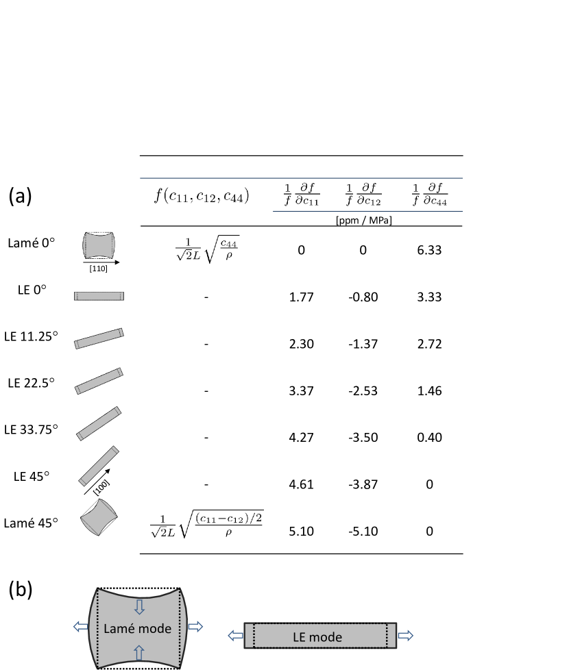
The frequency of an acoustic resonator is given by
| (1) |
where , and are the resonator material density, characteristic stiffness and characteristic length, respectively. The characteristic stiffness depends on the elastic constants , and that can be solved from a set of measured resonance frequencies of different resonance modes when their functional dependency on constants varies among the modes, and when there are three or more modes within the set. In our case, the set of two Lam mode resonators and five length extensional (LE) modes in different orientations fulfill these conditions. The test resonator set, and their exemplary sensitivities on the parameters are illustrated Fig. 1, and micrographs of the two types of resonators are shown in Fig. 3(a). Additional constraints that lead to the selection of this particular set of devices were: 1) the resonators had to be actuated electrostatically over vertical coupling gaps, 2) air damping needed to low enough to allow detection of resonances in atmospheric pressure, 3) the resonators had to be relatively large in lateral dimensions to minimize effects from processing inaccuracies, 4) the resonance frequencies and their sensitivities on should be insensitive to device thickness variations (see error in Section V-D), and 5) the number of different resonator types had to be relatively large in comparison with the three unknowns to allow assessment of the reliability of the results (Section V-C).
The experimental data consists of measured resonance frequencies at different temperatures for all seven resonance modes (). Let us denote the corresponding theoretical estimates containing the dependencies – obtained through FEM modelling – as . We use an approach of first matching and at by numerical minimization of
| (2) |
to find elastic parameters , and then linearize (1) to obtain the relation
| (3) |
Here are the unknown changes in elastic parameters, are the measured frequency differences, while and are shorthands for and . Sensitivities are calculated from the theoretical estimates. The last term accounts for thermal expansion, and it has been obtained by employing the isotropic of nature of length changes for silicon. We use a 3rd order expansion for this term
| (4) |
where values of , and are assumed. These expansion coefficients are based on the values reported for undoped silicon in Ref. [9]; thus, it is assumed that thermal expansion is not affected by doping. The assumption is supported by our measurements with mechanical dilatometry (see Section V-E).
In matrix form (3) can be denoted as
| (5) |
where contains the relative frequency changes, and elements of the sensitivity matrix are defined as
| (6) |
Sensitivity matrix elements are illustrated in Fig. 1. One should note that (6) depends on the linearization point at which it is evaluated.
The changes in elastic parameters can be solved as a least squares fit from (5):
| (7) |
II-B Numerical modelling
Numerical estimates of the modal frequencies were calculated by finite element analysis with Comsol Multiphysics. Resonance frequencies were obtained with modal analysis of full 3D geometries of the devices including the anchoring regions, see illustration of the finite element mesh in Fig 3(b). Nominal thickness of 15/24 of the wafers were used in the calculations, see Table I. Maximum size of the mesh elements was .
Calculation was performed for parameters , and spanning ranges of , and , respectively. The ranges were discretized to a grid of points. Values were stored in tables, and later retrieved for evaluation of Eqs. 2 and 6. Cubic interpolation was used for evaluation of between grid points. The discretization was verified to be dense enough for accurate evaluation of the derivatives of (6). Simulations took into account different angular misalignments of the wafers.
II-C Measurement of angular misalignment
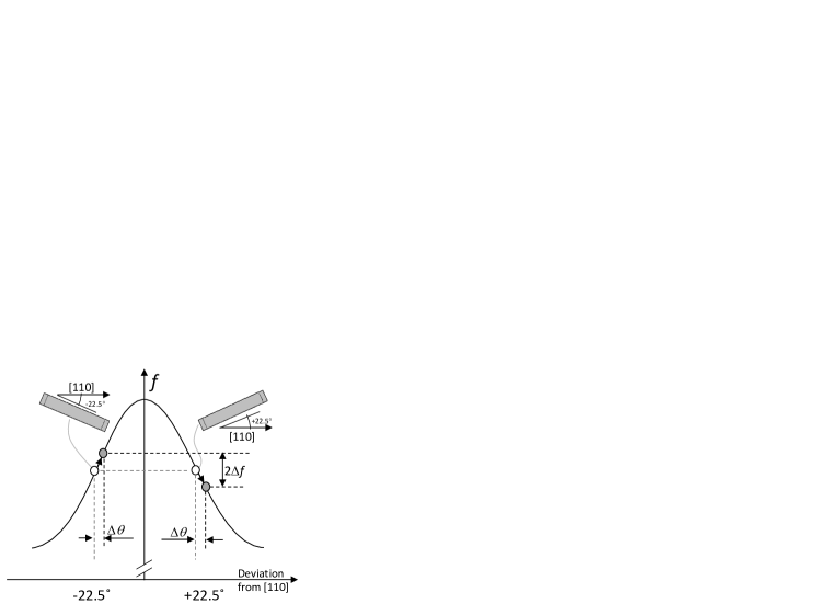
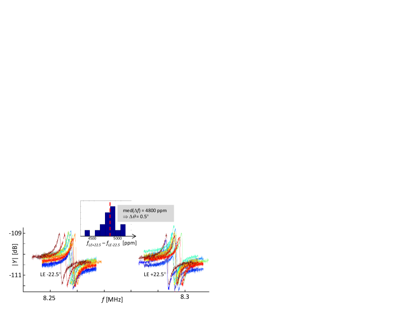
In practice, fabrication of the devices results in a small deviation of the resonator orientation from the intended alignment with the crystal axes, which can affect accuracy of the extraction of elastic parameters. This deviation, or angular misalignment , was determined using the method illustrated in Fig. 2. Due to silicon anisotropy, the resonance frequency of a LE mode beam resonator increases by ~10% when resonator alignment is rotated from [100] to [110]. Between these directions, i.e., at from [110], the resonance frequency is most sensitive to angular misalignment with Copies of two LE resonators identical in dimensions, but oriented to each other, both at the most sensitive orientation of were included on the wafers. The angular misalignment could be deduced from the up/down frequency shifts of these resonators.
III Experimental
![[Uncaptioned image]](/html/1401.1363/assets/x3.png)
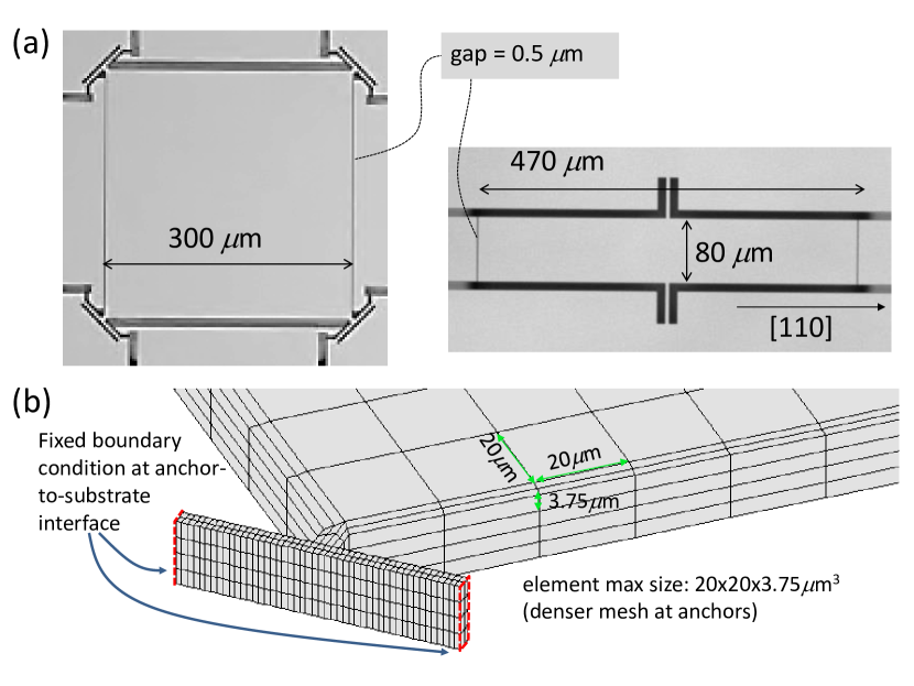
The resonators (Fig. 3(a)) were fabricated on seven different 150-mm C-SOI wafers (Silicon-On-Insulator wafers with pre-etched cavities [11]) manufactured in co-operation with Okmetic Oyj. The handle wafers with DRIE etched cavities were thermally oxidized before they were fusion bonded to the device wafers. Device layers were fabricated from 100-oriented wafers grown with the Czochralski method. The resonator fabrication process started with the C-SOI wafers with circular cavities of a diameter of for each resonator. The process flow consisted of two lithographic layers: 1) Al contact metallization and patterning 2) DRIE release etch producing vertical gaps of minimum nominal width of .
Dopant (B, P, and As) concentrations of the wafers for the silicon device layer were varied according to Table I. Carrier concentration range for each wafer was calculated from the specified resistivity range using conversion method of Ref. [10]. Device layer nominal thickness was 15 (24 for wafer B3), and the manufacturer specified C-SOI stack total thickness variation (including the handle wafer) was within for all wafers.
As the wafers featured pre-etched cavities, it was possible to fabricate monolithic resonators without a grid of release etch holes within the devices, and thus the elastic properties of the resonators could be accurately modelled. In our previous studies [5], existence of release etch holes was a source of uncertainty for the determination of the elastic constants.
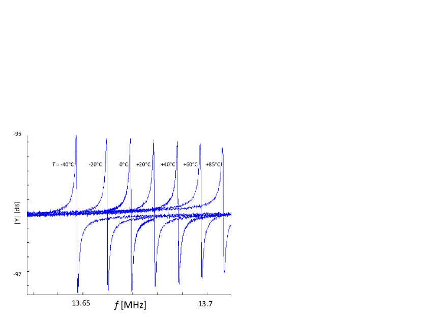
The resonators were measured on wafer level in atmospheric pressure on a Cascade Summit probe station using a HP 4294A impedance analyzer. A two-needle probe card was used for the measurements, and an open-short-load calibration was performed at in the beginning of the measurement. Measurements were done in the four-terminal pair configuration with four 2-m BNC cables, and the two end connections to the probe needles were long. A DC bias voltage of 40 V was applied between the resonator and the electrodes for electromechanical coupling. Effect on the resonance frequencies from the DC bias was negligible because of the relatively wide coupling gaps and the high mechanical spring constant of the resonance modes. The excitation AC voltage level was set to 1 V to maximize signal-to-noise ratio. The resonators still operated at their linear regime due to the weak electromechanical coupling. Measured devices were located near the wafer center. Quality factors of were measured for all resonance modes, and the resonance frequencies were extracted by fitting a BVD equivalent circuit to the the measured admittances. Example traces are shown in Fig. 4.
The wafer was held on a temperature controlled chuck, whose temperature was varied from -40∘C to +85∘C with seven steps (for wafer As1.7 the highest temperature was 80∘C). The specified temperature accuracy of the system (Temptronic TP3200A) including the temperature controller and the chuck was . A 15 minute stabilization period followed after each temperature change before probing of the resonators was started; the chuck temperature was well stabilized in less than 10 minutes for all temperature steps. Clean dry air flow at a rate of 30 l/min was used for purging. The effect from room temperature gas flow to resonator temperature was found to be smaller than the specified uncertainty of by the following comparison: Lame-45∘ resonator vs. curves on wafer B0.6 were compared to corresponding data from a similar wafer that was wafer level encapsulated by a silicon/glass wafer (encapsulation method is described in Ref. [12]). Encapsulated resonators can be assumed to be free from thermal gradients caused by the gas flow, but it could potentially affect temperature of resonators on uncapped wafers like B0.6. vs. curves of resonators near the wafer center on these two wafers were found to overlap with each other within ppm, implying that device temperatures were within C with each other (assuming identical temperature coefficients for the resonators on both wafers (see Table II).
IV Results
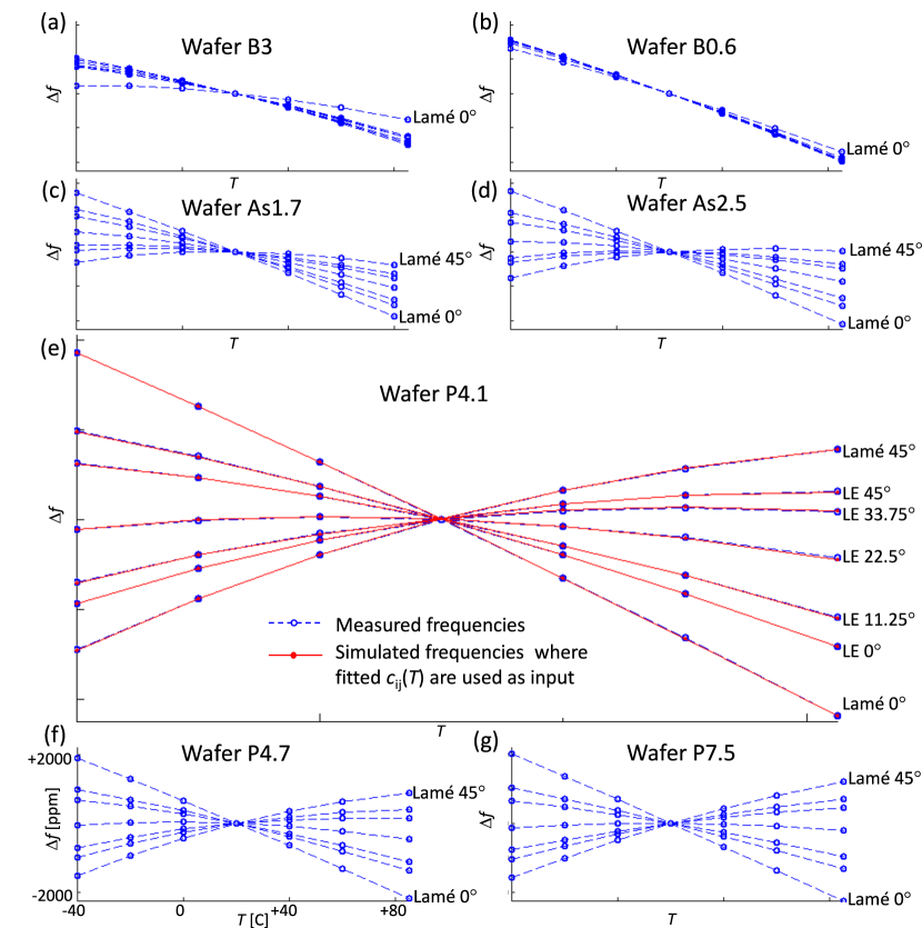
Measured frequency vs. temperature curves are shown for all modes on all wafers in Fig. 5, and the related temperature coefficients are collected in Table II.
![[Uncaptioned image]](/html/1401.1363/assets/x7.png)
On the weakest doped wafer B0.6 all vs. curves lie almost on top of each other, and the linear temperature coefficients are near -30 ppmK. On wafer B3 , the slopes of the curves are decreased in magnitude, and the biggest change is observed for the Lam - mode. On n-type doped wafers larger effects are observed. The slope of the vs. curve of the Lam - mode is gradually increased with increasing doping, and above the slopes are positive. Lame- mode is almost unaffected by doping, and the vs. curves of the LE modes span the region between the two Lam modes.
Frequencies of >20 LE beam resonators were measured on each wafer for determination of the angular misalignment as described in Section II-C. Results are tabulated in Table I. Figure 6 shows an example of the resonance curves for wafer P7.5.
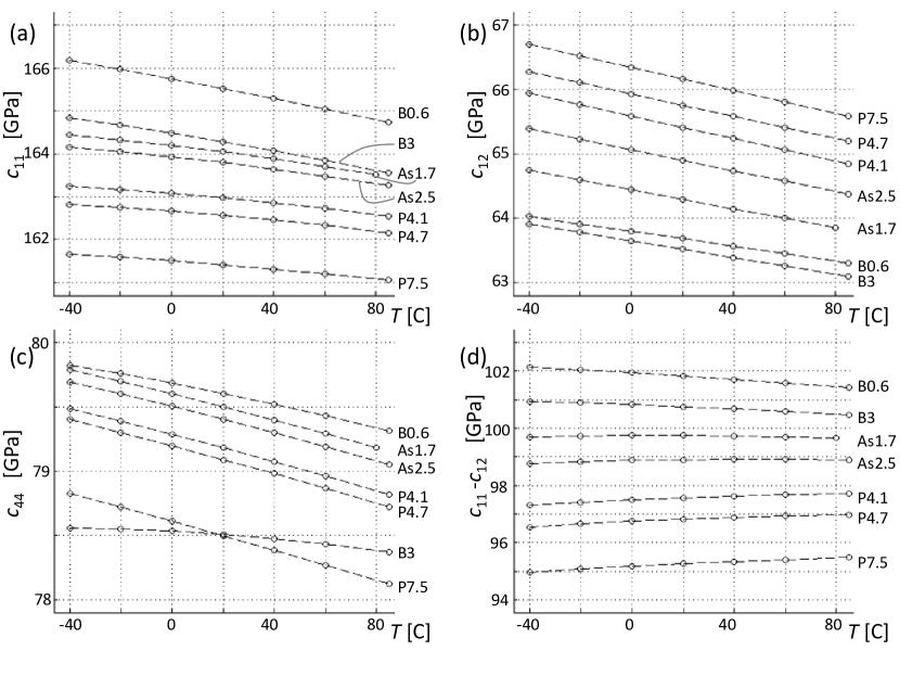
The elastic parameters were extracted from the measured frequency data using the least squares method of Section II-A. Results are shown in Fig. 7. The magnitude of the elastic constants is observed to decrease upon increased doping, except for the elastic constant which gets larger with increasing n-type doping.
For closer investigation of the thermal dependency of the curves, second-order polynomials centered at were fitted to the elastic parameter data as
| (8) |
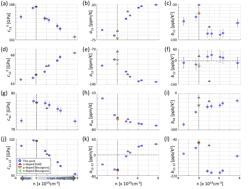
where and are the first-order and second-order temperature coefficients, respectively, and is the constant term111One should notice that the least squares method of Section II-A uses as the linearization point, since it was one of the measurement points. However, expansions of (8) and that of Table II are customarily centered at . A second-order expansion of was found to be valid to within for all . The results are collected in Figs. 8(a)–(l) and in Table III. One should note that, in Fig. 8, we have chosen to accommodate data points from both n- and p-type doped wafers within same axes by representing p/n type doping with negative/positive carrier concentrations. Observations are discussed in the following section.
![[Uncaptioned image]](/html/1401.1363/assets/x11.png)
V Discussion
V-A Comparison to literature
Temperature coefficients measured in this work are compared to previously reported values in Fig. 8. Values for relatively weakly n- or p-doped silicon, reported by Bourgeois et al. [13], appear to be in satisfactory agreement with our data; the data points near zero carrier concentration follow the trends observable from our data points. Data by Hall [8] differs somewhat from our results, in particular for the second order temperature coefficients. However, it should be noted that the temperature coefficients for Hall’s data are based on graphical extraction of the published curves.
V-B Behavior of elastic coefficients with doping
Figs. 8(a), (d), (g) and (j) show that the magnitude of the elastic parameters, i.e., the constant terms , are affected to within a few percent by increased doping over the tested wafers. These changes need to be taken into account when dimensioning resonator designs targeting a specific resonance frequency. While the offsets have a negligible effect for temperature compensation purposes, it has the potential to degrade the initial frequency accuracy within a set of devices on a single wafer or within a batch of wafers.
In general, it is seen that arsenic (data points with ) and phosphorus () as dopants do not stand out from the plots as separate groups, which supports the view of the effects being of mainly electronic origin[1].
The effects on silicon elastic properties from n-type doping are best observed in the shear elastic constant and, in particular, in its temperature coefficients and . Fig. 8(k) shows that the linear temperature coefficient crosses zero at approximately . This is the effect of most practical importance for temperature compensation of MEMS applications, since many shear-type resonance modes are purely dependent on the term, and hence the linear temperature coefficient of frequency of such resonators can be brought to zero at this doping level. For example, the Lame mode of Fig 1(a) is a mode whose frequency depends solely on . When doping is further increased, reaches a level of over . The effect appears to saturate with increasing doping. A wide class of resonance modes, such as torsional, flexural and extensional modes have an amount of shear mode character, i.e., their frequency depends on with a large weight factor. Thus, their vs. curves are largely determined by the behavior of the term. The fact that attains relatively large positive values enables first-order temperature compensation of such modes. These aspects are discussed in more detail in Ref. [6].
Fig. 8(l) shows that the second order coefficient is negative for all studied doping levels, with a maximum deviation from zero of approximately . This would translate to a 250 ppm frequency deviation over a range of 100∘C. Importantly, one finds that the second order coefficient appears to approach zero when n-type doping level is above . This suggests a possibility of a flat or positive second order response at high enough doping, motivating further investigation of n-type doping beyond .
The key effect to temperature compensation with p-type doping is observable in Fig. 8(h). The linear temperature coefficient approaches zero with increasing p-type dopant concentration. However, zero level is not yet crossed with the highest doping level of . The second order coefficient is seen to grow in magnitude with increased p-type doping. N-type doping is observed to have a relatively small effect on coefficients and
V-C Reliability of elastic parameter extraction
Seven data points were used for the extraction of the three unknown elastic parameters at each temperature. Hence, the reliability of the method can be assessed by comparing the measured frequency data to the corresponding numerical estimates obtained from FEM simulations which use the solved parameters as an input. First, Fig. 9(a) shows the correspondence of measured and simulated resonance frequencies at , where has been obtained from a fit to (2). The difference is within
Correspondingly, the quality of the least squares fit of (7) can be judged from the overlap of the measured and simulated data, exemplified in Fig. 5(e). This is seen in closer detail in Fig. 9(b), where the difference between the measured relative frequency changes and the corresponding theoretical estimates has been plotted for all modes on all wafers. Maximum deviation between the measured and simulated data points was below for all seven resonance modes on all wafers, which speaks for the reliability of the extraction method. It should be noted that without correction of the angular misalignments (Section II-C), the least squares method would have resulted in errors up to 60 ppm.
Validity of the linearization step needed for the least square method was confirmed: Frequency changes from approximation of (3) were calculated for each of the extracted elastic parameters , and compared with the non-linearized counterpart . Linearization error was found to be less than 5 ppm for all cases.
Based on the above analysis, we expect that by using the extracted elastic parameters, one can estimate the frequency of an arbitrary resonance mode, fabricated on a wafer with similar carrier concentration as in our experiments, with following accuracies:
-
•
Absolute frequency of a resonator can be predicted with accuracy.
-
•
Thermal drift over a temperature range of can be predicted with accuracy.
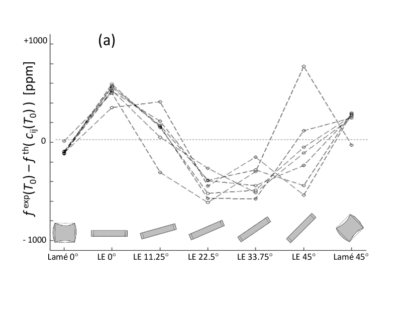
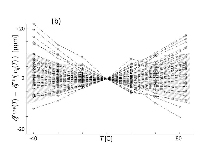
Figure 9: (a) Difference between measured frequencies and theoretical estimates ) at for all resonance modes on all wafers. Theoretical estimates are based on , which are the fitted elastic parameters obtained through numerical minimization of (2). (b) Difference between the measured relative frequency changes and the corresponding theoretical estimates for all resonance modes on all wafers. Theoretical estimates are calculated using that have been fitted using (7). The shaded region illustrates the frequency measurement uncertainty that has been assumed in error analysis of Section V-D.
V-D Accuracy of temperature coefficients of parameters
While the analysis of the previous section provides a way to establish a confidence level on the resonance frequencies that can be calculated from the extracted elastic parameters of this work, one can obtain also estimates for the accuracy of the temperature coefficients of elastic constants. Let us denote these confidence intervals as , and They are listed in Table III and also shown as vertical error bars in Fig. 8.
For , an upper limit of is obtained by starting from the above discussed absolute frequency accuracy of , and by applying (1). Other potential error sources of smaller magnitude are:
-
•
The mass of dopant atoms differs from that of silicon. Assuming that the volume of the crystal stays constant the maximal density change is less than 200 ppm, which would be reflected as a similar inaccuracy in .
-
•
The dimensions of the resonators may vary slightly from the designed measures due to potential mask bias and imperfections in DRIE etching. A conservative estimate for the lateral dimension change of of the resonators would deviate the resonance frequency approximately by ppm, and thus have an effect of on .
-
•
Thickness variation of of the device layer would have a very small effect on frequencies of the resonators: FEM analysis indicated that the frequencies of the LE modes stay within , and changes are even smaller for the Lam modes.
To assess the inaccuracy of the first and second order temperature coefficients of the elastic parameters, a Monte Carlo approach was used to simulate the effect of several error sources. A large number of copies of the experimental data sets (of Fig. 5) were taken, and perturbed according to following sources of uncertainty, labeled as :
: Relative frequencies were deviated by where was taken from a normally distributed population with a standard deviation of 10 ppm, was defined as , and was set to . The distribution is visualized by the shaded region of Fig. 9(b)). This way a distribution corresponding to the observed errors in relative frequencies was reproduced.
: The accuracy specified for the temperature controller and chuck was taken into account by deviating the temperature points by taken from a normally distributed population with a standard deviation of .
: Sensitivities of (6) were evaluated at the linearization points , which was estimated above to have an uncertainty within . Error caused by this was simulated by perturbing the linearization points accordingly.
: Thermal expansion was assumed constant in the calculations, and our measurements suggested this to hold for linear thermal expansion within a error marginal (V-E). The thermal expansion effect in (4) was perturbed to take this uncertainty into account.
: Thickness of the devices deviated from the nominal thicknesses used in the simulations. Sensitivities of (6) were perturbed to take into account a thickness variation of .
Extraction of the elastic parameters was performed on the perturbed data sets, identically to as it was done on the real measurement data, and distributions of and were obtained. Confidence intervals and were calculated for each error source separately, and the total effect was estimated as the rms sum. Values for and were obtained as standard deviations the / distributions, while the full range was used for . Inaccuracy of the first order coefficient was found to range from to . Correspondingly, error of the second order coefficient was seen to vary from to Error in measured frequencies () and inaccuracy of temperature () were major sources of uncertainty for all parameters, and the linearization point error () was a top contributor for and .
V-E Doping independency of thermal expansion
The procedure for extracting the elastic parameters relied on the assumption that thermal expansion of (4) would be insensitive to doping. To our knowledge, effects from heavy doping to thermal expansion of silicon have not been studied experimentally. For verification, mechanical dilatometry was used for measuring the thermal expansion of samples with similar doping levels as wafers B3, As1.7 and P7.5. The linear thermal expansion coefficient was found to be constant within the error marginal of the measurement.
V-F Manufacturability of temperature compensated MEMS resonators
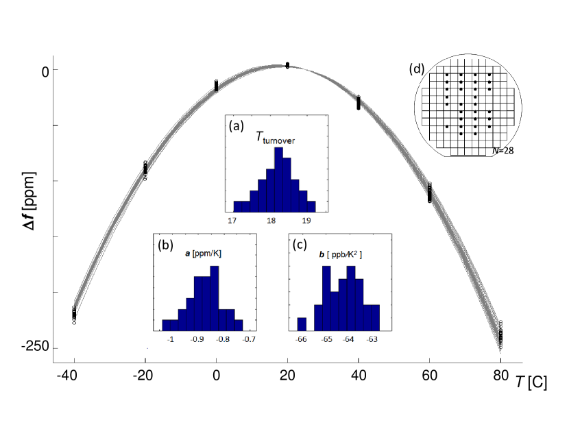
Eventual manufacturability of silicon resonators whose temperature compensation is based on degenerate doping crucially depends on the statistical variations of the vs. curves among devices fabricated on a single wafer or on a batch of wafers. This aspect was addressed by studying a set of ~30 square extensional mode resonators of Ref. [5], which were fabricated on a wafer with a specification similar to that of wafer P4.7 of this work. The vs. curves of the devices are shown in Fig. 10. These devices were temperature compensated to first order with their turnover temperatures near . The overall frequency drift over the whole temperature range of stays within 250 ppm, and maximum deviation between samples is approximately 20 ppm. One should note that the data of this example is from devices on a Czochralski grown wafer, where the doping level may vary within the wafer. A better control of doping level is achievable with diffusion based doping, or with epitaxially grown silicon, where doping can be controlled during the crystal growth process.
VI Conclusion
Elastic constants , and of degenerately doped silicon were studied experimentally as a function of the doping level and temperature. First and second order temperature coefficients of the elastic constants were extracted from measured resonance frequencies of a set of MEMS resonators fabricated on wafers with varied doping.
The linear temperature coefficient of the shear elastic parameter was found to be zero at n-type doping level of . It was observed to increase to over with higher level of doping, which implies that the frequency of many types of resonance modes, including extensional bulk modes and flexural modes, can be temperature compensated to first order. The second order temperature coefficient of was found to decrease by 40% in magnitude when n-type doping was increased from 4.1 to , suggesting a further reduction of the second order effect with increased doping.
It was found that the frequency drift of an arbitrary silicon resonator design, fabricated on a wafer with doping level similar to those investigated in this work, can be estimated with an accuracy of ppm over a temperature range of using the elastic parameters of this work. Absolute frequency can be calculated with an accuracy of ppm.
VII Acknowledgments
The authors would like to acknowledge the Finnish Funding Agency for Technology and Innovation (Tekes), Okmetic Oyj, Murata Electronics and Micro Analog Systems for funding. Okmetic Oyj is acknowledged for providing the silicon wafers. A.J. acknowledges funding from the Academy of Finland, and wishes to thank Arto Nurmela for help in the measurements. Roger Morrell is thanked for performing the thermal expansion measurements.
References
- [1] R. W. Keyes, “Electronic effects in the elastic properties of semiconductors,” in Solid State Physics: Advances in Research and Applications, ed. by F. Seitz and D. Turnbull. Academic Press, 1967, vol. Volume 20, pp. 37–90.
- [2] F. S. Khan and P. B. Allen, “Temperature dependence of the elastic constants of p+ silicon,” Physica Status Solidi (b), vol. 128, no. 1, pp. 31–38, 1985.
- [3] A. K. Samarao, G. Casinovi, and F. Ayazi, “Passive TCF compensation in high q silicon micromechanical resonators,” in IEEE International Conference on Micro Electro Mechanical Systems (MEMS 2010), Hong Kong, Jan. 2010, pp. 116–119.
- [4] A. Hajjam, A. Rahafrooz, and S. Pourkamali, “Sub-100ppb/C temperature stability in thermally actuated high frequency silicon resonators via degenerate phosphorous doping and bias current optimization,” in Proc. IEEE International Electron Device Meeting (IEDM), 2010, pp. 7.5.1 – 7.5.4.
- [5] T. Pensala, A. Jaakkola, M. Prunnila, and J. Dekker, “Temperature compensation of silicon MEMS resonators by heavy doping,” in Proc. IEEE International Ultrasonics Symposium, 2011, pp. 1952–1955.
- [6] A. Jaakkola, M. Prunnila, and T. Pensala, “Temperature compensated resonance modes of degenerately n-doped silicon MEMS resonators,” in Frequency Control Symposium (FCS), 2012 IEEE International, May 2012, pp. 1 –5.
- [7] E. J. Ng, C. H. Ahn, Y. Yang, V. A. Hong, C.-F. Chiang, E. Ahadi, M. W. Ward, and T. W. Kenny, “Localized, degenerately doped epitaxial silicon for temperature compensation of resonant MEMS systems,” in Transducers 2013, Barcelona, Spain, 2013, pp. 2419—2422.
- [8] J. J. Hall, “Electronic effects in the elastic constants of n-type silicon,” Physical Review, vol. 161, no. 3, p. 756, 1967.
- [9] K. G. Lyon, G. L. Salinger, C. A. Swenson, and G. K. White, “Linear thermal expansion measurements on silicon from 6 to 340 k,” Journal of Applied Physics, vol. 48, no. 3, pp. 865–868, Mar. 1977.
- [10] “Standard practice for conversion between resistivity and dopant density for boron-doped, phosphorus-doped, and arsenic-doped silicon,” in Annual Book of ASTM Standards, F 723-99. West Conshohocken, PA: American Society for Testing and Materials, 2000, pp. 275—291.
- [11] H. Luoto, K. Henttinen, T. Suni, J. Dekker, J. M kinen, and A. Torkkeli, “MEMS on cavity-SOI wafers,” Solid-State Electronics, vol. 51, pp. 328–332, 2007.
- [12] V. Kaajakari, J. Kiiham ki, A. Oja, S. Pietik inen, V. Kokkala, and H. Kuisma, “Stability of wafer level vacuum encapsulated single-crystal silicon resonators,” Sensors and Actuators A: Physical, vol. 130, pp. 42–47, 2006.
- [13] C. Bourgeois, E. Steinsland, N. Blanc, and N. F. de Rooij, “Design of resonators for the determination of the temperature coefficients of elastic constants of monocrystalline silicon,” in IEEE International Frequency Control Symposium, 1997, pp. 791–799.