Electronic and Thermoelectric Properties of Few-Layer Transition Metal Dichalcogenides
Abstract
The electronic and thermoelectric properties of one to four monolayers of MoS2, MoSe2, WS2, and WSe2 are calculated. For few layer thicknesses, the near degeneracies of the conduction band and valleys and the valence band and valleys enhance the n-type and p-type thermoelectric performance. The interlayer hybridization and energy level splitting determine how the number of modes within of a valley minimum changes with layer thickness. In all cases, the maximum ZT coincides with the greatest near-degeneracy within of the band edge that results in the sharpest turn-on of the density of modes. The thickness at which this maximum occurs is, in general, not a monolayer. The transition from few layers to bulk is discussed. Effective masses, energy gaps, power-factors, and ZT values are tabulated for all materials and layer thicknesses.
I INTRODUCTION
Semiconducting, transition-metal dichalcogenides (TMDCs) exhibit promising electronic Radisavljevic et al. (2011); Yoon et al. (2011); Fang et al. (2012); Alam and Lake (2012); Han Liu and Ye (2012), opto-electronic Li and Galli (2007) and spintronic Xiao et al. (2012) properties. Single monolayers (three atomic layers) can be either exfoliated or grown with chemically stable surfaces. The electronic, optical, and spin properties of monolayers are qualitatively different from those of the bulk. The band gap changes from indirect to direct, and the valence band edges at the and points become spin polarized.Li and Galli (2007); Xiao et al. (2012) These materials are discussed in a number of recent reviews.Novoselov and Neto (2012); Wang et al. (2012); Geim and Grigorieva (2013); Xu et al. (2013); Butler et al. (2013)
Experimental studies conducted on a different set of two-dimensional materials, namely Bi2Te3 and Bi2Se3, demonstrated an improvement in their thermoelectric performance as their thickness was reduced. Sun et al. (2012); Goyal et al. (2010) A large increase in ZT has been theoretically predicted for monolayer Bi2Te3 compared to that of the bulk.Ghaemi et al. (2010); Zahid and Lake (2010); Maassen and Lundstrom (2013) This enhancement in ZT results from the unique, step-function shape of the density of modes at the valence band edge of a single quintuple layer.Zahid and Lake (2010); Maassen and Lundstrom (2013) The shape of the density of modes increases the power factor, and the increase in the power factor increases ZT. For Bi2Te3, the large enhancement in the power factor and in ZT only occurs for a monolayer. For bilayer and trilayer Bi2Te3, the step-like shape of the density of modes disappears, and the calculated values of ZT are either slightly higherF.Zahid and R.K.Lake or slightly lowerMaassen and Lundstrom (2013) than that of the bulk.
Prior experimental and theoretical investigations of the thermoelectric performance of transition metal dichalcogenides have focused on either bulk or monolayer materials. Amara et al. (1987); Imai et al. (2001); Guo et al. (2013); Li and Galli (2007); Buscema et al. ; Huang et al. (2013); Lee et al. (2013). There has not been a study of the effect of film thickness on the power factor and ZT in the transition metal dichalcogenides. It is not known whether the power factor and ZT are maximum at monolayer thickness or at some other thickness.
This work theoretically investigates the electronic properties and the thermoelectric performance of bulk and one to four monolayers of 4 different TMDC materials: MoS2, MoSe2, WS2, and WSe2. The goal is to understand how their electronic and thermoelectric properties vary with thickness. Similar to monolayer Bi2Te3, the increase in ZT for the ultrathin films results from an enhanced degeneracy or near-degeneracy of the band edges. In the TMDCs, at few layer thicknesses, different valleys become nearly degenerate with energy differences of less than at room temperature. Because of weak interlayer coupling at certain valleys, additional bands from additional layers lie within of the bandedges for few layer thicknesses. The increased degeneracy results in a sharper turn on of the the density of modes near the band edges. In all cases, the thickness with the sharpest increase in the density of modes has the largest value for ZT. For the semiconducting TMDCs considered here, that optimum thickness is not, in general, a single monolayer.
II THEORETICAL METHODS
Ab-initio calculations of the bulk and few-layer structures (one to four layers) are carried out using density functional theory (DFT) with a projector augmented wave method Blöchl (1994) and the Perdew-Burke-Ernzerhof (PBE) type generalized gradient approximation Perdew et al. (1996); Ernzerhof and Scuseria (1999) as implemented in the Vienna ab-initio simulation package (VASP). Kresse and Hafner (1993); Kresse and Furthmuller (1996) The vdW interactions in MoSe2 and MoS2 are accounted for using a semi-empirical correction to the Kohn-Sham energies when optimizing the bulk structures (optimization of WS2 and WSe2 structures are done at the PBE level since the semi-empirical parameters for tungsten are currently not described by the dispersion potential).Grimme (2006) The Monkhorst-Pack scheme is used for the integration of the Brillouin zone with a k-mesh of 12 x 12 x 6 for the bulk structures and 12 x 12 x 1 for the thin-films. The energy cutoff of the plane wave basis is 300 eV. All of the the electronic bandstructure calculations include spin-orbit coupling. Calculations are also performed without spin-orbit coupling and the results are compared.
To verify the results of the PBE calculations, the electronic structure of 1L, 2L, 3L and 4L MoS2 are calculated using the much more computationally expensive hybrid Heyd-Scuseria-Ernzerhof (HSE) functional.Heyd et al. (2003) The HSE calculations incorporate 25 short-range Hartree-Fock exchange. The screening parameter is set to 0.4 .
The thermoelectric parameters are calculated from a Landauer formalism using the ab-initio derived density of modes.Zahid and Lake (2010); Maassen and Lundstrom (2013); Huang et al. (2013) In the linear response regime, the electronic conductivity (), the electronic thermal conductivity (), and the Seebeck coefficient (S) are expressed as Jeong et al. (2010); Paul et al. (2012)
| (1) | |||||
| (2) | |||||
| (3) | |||||
| (4) |
where is the device length, is the magnitude of the electron charge, is Planck’s constant, and is Boltzmann’s constant. The transmission function is
| (5) |
where M(E) as the density of modes (DOM). In the diffusive limit,
| (6) |
and is the electron mean free path. When phonon scattering is dominant, the mean free path can be written as a constant, . As discussed in Ref. [Kim et al., 2009], the transport distribution, , arising from the Boltzmann transport equation is related to the above quantities by .
The density of modes M(E) can be defined as Maassen and Lundstrom (2013); Jeong et al. (2010)
| (7) |
where is the dimensionality of the system, are the dimensions of the structure perpendicular to the direction of transport ( = W x t for d = 3, = W for d = 2; W = width of the structure, t = film thickness), is the unit step function, and refers to the states in the first Brillouin zone perpendicular to the transport direction. Using Eq. (7), M(E) of any material in any dimension can be numerically evaluated from a given electronic band structure by counting the bands that cross the energy of interest. The density of modes calculations are performed by integrating over the first Brillouin zone using a converged k point grid (51 x 51 x 10 k points for the bulk structures and 51 x 51 x 1 for the thin films).
We account for carrier scattering within each structure by fitting our calculated bulk electrical conductivity with bulk experimental data. An electron mean free path of = 14 nm gives the best agreement with experimental data on the Seebeck response of bulk MoS2 as a function of the electrical conductivity.Mansfield and Salam (1953); Thakurta and Dutta (1983) The bulk p-type electrical conductivity of MoS2 at room temperature was reported to be 5.1 cm-1 with a Seebeck coefficient of 450 VK-1 at a carrier concentration of 1016 cm-3.Thakurta and Dutta (1983) Using = 14nm we obtain an electrical conductivity of 4.97 cm-1 with a Seebeck coefficient of 398 VK-1 at the same carrier concentration. This value of the mean free path is also consistent with a theoretically derived energy independent acoustic phonon-limited mean free path ( = 14 nm) for electrons in monolayer MoS2,Kaasbjerg et al. (2012) and was successfully used to simulate and compare to experimental results of the transfer characteristics of single layer MoS2 field effect transistor.Yoon et al. (2011) As an initial approximation of carrier scattering we use the same value to model the thermoelectric properties of all the TMDC materials investigated in this study.
For the in-plane lattice thermal conductivity, a value of 19.5 obtained from a molecular dynamics simulation on monolayer MoS2 is used.Varshney et al. (2010) Prior experimentalChiritescu et al. (2007) and theoreticalHuang et al. (2013) studies of the lattice thermal conductivity in the TMDC materials have demonstrated that does not vary significantly for the different TMDC compounds studied here. With the above quantities in hand, the power factor, , and the thermoelectric figure of merit are determined.
III RESULTS
All of the thermoelectric parameters are derived from the calculated electronic bandstructures. Therefore, we begin this section with a discussion of the calculated bandstructures. The bandstructure calculations produce considerably more information than is required for calculating the thermoelectric parameters. To preserve that information and contribute towards a database of material parameters, extracted properties such as effective masses and energy gaps at high symmetry points are tabulated.
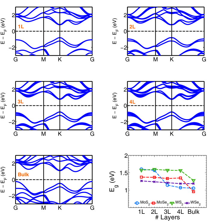
Figure Electronic and Thermoelectric Properties of Few-Layer Transition Metal Dichalcogenides shows the ab-initio band structure of one-layer (1L) through four-layer (4L) and bulk WS2. The large valence band splitting at the -point and the direct-indirect gap transition as the film thickness increases above 1L are features that occur in the other TMDC materials included as part of this study. The last panel in Fig. Electronic and Thermoelectric Properties of Few-Layer Transition Metal Dichalcogenides illustrates the effect of decreasing layer thickness on the bandgap for all of the materials studied. The optimized lattice parameters of the bulk TMDC compounds are listed in Table 1. The results in Table 1 and Figure Electronic and Thermoelectric Properties of Few-Layer Transition Metal Dichalcogenides are consistent with prior experimental characterization Bronsema et al. (2004); Schutte et al. (1987); Kam and Parkinson (1982) and theoretical calculations of the bulkJiang (2012); Coehoorn et al. (1987) and thin filmDing et al. (2011a); Kuc et al. (2011a) crystal structures and electronic band structures. The results of these electronic structure calculations at the high symmetry points are summarized in Tables 2 and Table 3. Table 2 gives the relative effective masses, and Table 3 gives the energy gaps.
A number of prior theoretical studies of the electronic structure of monolayer and few-layer TMDCs did not include spin-orbit interaction. Liu et al. (2011); Kuc et al. (2011b); Ding et al. (2011b) As a result, the band bandgaps reported in those studies are slightly larger. For example the bandgaps reported in a prior PBE level calculation Ding et al. (2011b) are greater by 70 meV, 260 meV and and 284 meV for MoS2 and MoSe2, WS2 and WSe2 respectively when compared to our calculation results. Without the inclusion of spin-orbit interaction, our values for the bandgap of the monolayer TMDCs are consistent with the bandgaps reported in these studies. Including spin-orbit coupling results in a splitting of the valence bands, , at . The spin orbit interaction shifts up one of the degenerate valence bands, and this reduces the bandgap. The degree of the energy shift ranges from 39.6 meV for MoS2 to 210.9 meV for WS2. The second degenerate valence band is shifted down by an energy that is also unique to each TMDC material; this ranges from 110.4 meV for MoS2 to 316.2 meV for WSe2. For example the calculated energies of the monolayer TMDCs are 150 meV, 181 meV, 425 meV and 461 meV for MoS2, MoSe2, WS2 and WSe2, respectively. This is in good agreement with a prior PBE level calculation Ramasubramaniam (2012) that accounted for spin-orbit interaction which obtained values of 146 meV, 183 meV, 425 meV and 461 meV for MoS2, MoSe2, WS2 and WSe2, respectively, and a energy of 188 meV obtained for monolayer MoS2 with the use of optical absorption experiments. Mak et al. (2010)
More sophisticated many-body ab-initio calculations which include HSE or GW calculations have been reported in prior studies of the band structure of monolayer Cheiwchanchamnangij and Lambrecht (2012); Ramasubramaniam (2012); Shi et al. (2013); Zahid et al. (2013a) and bilayer Cheiwchanchamnangij and Lambrecht (2012); Zahid et al. (2013a) structures of the molybdenum and tungsten dichalcogenides. The values for resulting from these theories are only slightly changed from those of the PBE model. The values reported for monolayer MoS2, MoSe2, WS2 and WSe2 with a GW (HSE) calculation are 164 (193) meV, 212 (261) meV, 456 (521) meV and 501 (586) meV.Ramasubramaniam (2012) The primary difference between the PBE and the HSE and GW calculations is an increase in the bandgap. However, the PBE bandgap is large enough compared to the temperatures considered that the exact magnitude of the bandgap has no effect on the thermoelectric parameters. An explicit comparison of the electronic structure and the thermoelectric parameters calculated from the PBE and the HSE functionals for 1L - 4L MoS2 is given below.
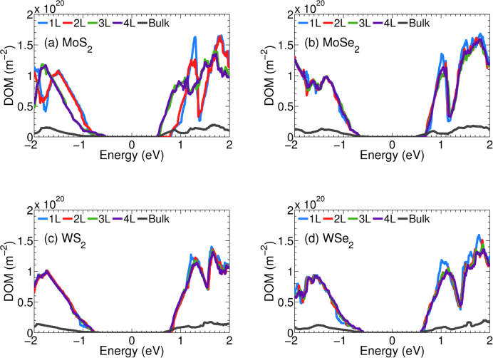
Calculation of the thermoelectric parameters requires the density of modes extracted from the electronic bandstructure using Eq. (7). Figure Electronic and Thermoelectric Properties of Few-Layer Transition Metal Dichalcogenides shows the density of modes versus energy for bulk, 1L, 2L, 3L, and 4L MoS2, MoSe2, WS2, and WSe2. To compare the density of modes of the bulk structure with the thin-film structures, we divide the density of modes of the thin-film structures by their respective thickness, . As will be shown, for these TMDCs, small variations in the shape of the density of modes near the band edges can enhance the power factor and subsequently ZT. The thermoelectric properties of the bulk and thin-film structures are calculated from Eqs. (1) - (6) using the density of modes shown in Fig. Electronic and Thermoelectric Properties of Few-Layer Transition Metal Dichalcogenides.
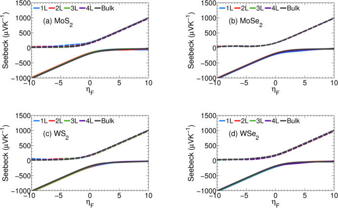
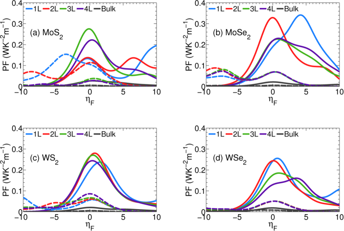
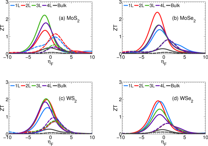
The Seebeck coefficient, electrical conductivity, power-factor (PF), and the thermoelectric figure-of-merit (ZT) as a function of the reduced Fermi level, are shown in Figures Electronic and Thermoelectric Properties of Few-Layer Transition Metal Dichalcogenides, Electronic and Thermoelectric Properties of Few-Layer Transition Metal Dichalcogenides, Electronic and Thermoelectric Properties of Few-Layer Transition Metal Dichalcogenides, and Electronic and Thermoelectric Properties of Few-Layer Transition Metal Dichalcogenides, respectively. The reduced Fermi-level is for electrons in the conduction band, and for holes in the valence band. and are the energies of the conduction and valence band edges, respectively. For each material and each thickness the maximum power factor and ZT occurs for the conduction band states. The peak conduction band and valence band power factor and ZT for each structure and material at 77K, 150K and 300K are summarized in Table 4 and Table 5, respectively. For all materials, the few layer structures show a large increase in the values of their power factor and ZT compared to those of the bulk.
The peak n-type ZT values (and corresponding layer thicknesses) for MoS2, MoSe2, WS2 and WSe2 are 2.23 (t=3L), 2.39 (t=2L), 2.03 (t=3L) and 1.91 (t=2L) which is an improvement by a factor of 6.4, 8.2, 7.2 and 7.5 over the respective bulk values. These peak ZT values occur when the Fermi level is moved by 1.39kT, 1.55kT, 1.08kT and 1.39kT, respectively, below the conduction band at T=300K. This corresponds to electron carrier densities of 6.26 1019 cm-3, 5.74 1019 cm-3, 5.34 1019 cm-3 and 4.72 1019 cm-3 for MoS2, MoSe2, WS2 and WSe2 respectively. The peak p-type ZT values (and corresponding layer thicknesses) for MoS2, MoSe2, WS2 and WSe2 are 1.15 (t=2L), 0.81 (t=2L-4L), 0.76 (t=2L-3L) and 0.62 (t=1L-4L) which is an improvement by a factor of 14.4, 10.1, 9.5 and 5.2 over the respective bulk values. These peak ZT values occur when the Fermi level is moved by 1.16kT, 1.01kT, 0.93kT and 0.85kT, respectively, above the valence band at T=300K. This corresponds to hole carrier densities of 7.12 1019 cm-3, 5.84 1019 cm-3, 4.02 1019 cm-3 and 3.91 1019 cm-3 for MoS2, MoSe2, WS2 and WSe2 respectively. Of the four TMDC materials studied, MoS2 is the only material to exhibit a p-type and n-type ZT 1. In contrast to Bi2Te3, the peak value of ZT does not occur in any of the materials at a monolayer thickness.
The Seebeck coefficients at the maximum n-type (p-type) ZT for each material are 275 (245.6) VK-1, 287 (230.7) VK-1, 279 (230.1) VK-1 and 276 (216.7) VK-1 for MoS2, MoSe2, WS2 and WSe2 respectively. However, the Seebeck coefficients at the maximum n-type (p-type) power factor for each material are 167 (90.4) VK-1, 100 (185.8) VK-1, 165 (177.1) VK-1 and 171 (172.1) VK-1 for MoS2, MoSe2, WS2 and WSe2, respectively. This is generally consistent with the conclusion of a report on engineering the Seebeck coefficient to obtain the maximum thermoelectric power factor. Pichanusakorn and Bandaru (2009)
Without the inclusion of spin-orbit interaction our values of the ballistic ZT for the monolayer TMDC materials are consistent with a prior report on the monolayer thermoelectric properties of these TMDC materials.Huang et al. (2013) Our calculations show that without the inclusion of spin-orbit interaction the peak n-type ZT values for all materials continue to occur at thicknesses above a single monolayer. The peak n-type ZT values (and corresponding layer thicknesses) without spin-orbit interaction for MoS2, MoSe2, WS2 and WSe2 are 1.38 (t=3L), 1.52 (t=2L), 1.13 (t=4L) and 1.28 (t=2L). However, the peak p-type ZT values without spin-orbit interaction occurs for a single monolayer for each TMDC material. The p-type ZT values without spin-orbit interaction for MoS2, MoSe2, WS2 and WSe2 are 1.42, 0.84, 0.90 and 0.69.
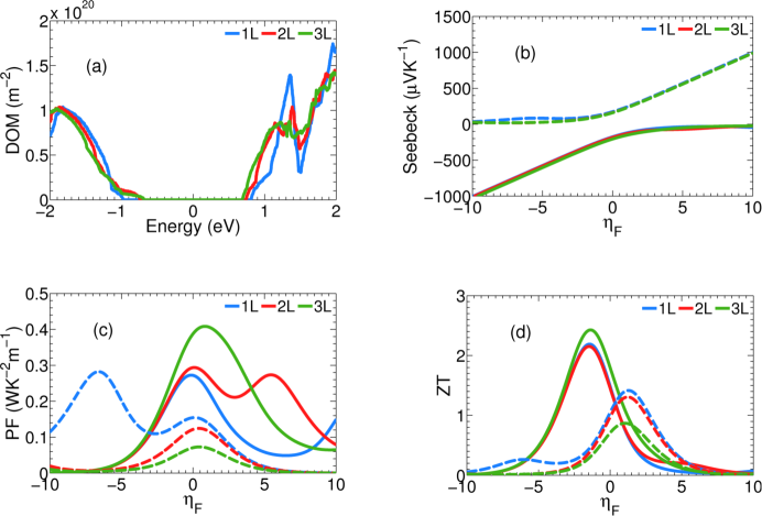
Recent electronic structure calculations using the Heyd-Scuseria-Ernzerhof (HSE) hybrid functional Zahid et al. (2013b) give a bandgap that more accurately matches known experimental values.Zahid et al. (2013b) To assess whether the trends in the thermoelectric parameters predicted with the PBE functional are the same as those resulting from the HSE functional, we calculate the electronic band structure of 1L, 2L, 3L and 4L MoS2 with both the PBE and the HSE functional and plot the results in Fig. Electronic and Thermoelectric Properties of Few-Layer Transition Metal Dichalcogenides. Near the band edges, the HSE energies appear to be shifted with respect to the PBE energies. The effective masses for the HSE band structures are lower by up to 17 for the conduction band valleys at and and are lower by up to 11 for the valence band valleys at and .
To verify that the HSE functional leaves the thermoelectric trends predicted from the PBE functional unchanged, we compute the density-of-modes and thermoelectric performance of 1L, 2L and 3L MoS2 using the HSE functional with the inclusion of spin orbit coupling. Figure Electronic and Thermoelectric Properties of Few-Layer Transition Metal Dichalcogenides illustrates the DOM, Seebeck coefficient, power factor and ZT for the 1L, 2L and 3L structures of MoS2 computed with the HSE functional. The quantitative values do differ. For the MoS2 trilayer structure, the HSE (PBE) functionals give a peak n-type power factor of 0.41 (0.28) WK-2m-2 and a peak n-type ZT of 2.4 (2.2). However, the HSE results for few-layer MoS2 structures demonstrate the same trends in the shape of the density of modes and the same trends in the values for the power factors and ZT. Both the HSE and PBE calculations show that the turn-on of the density of modes is sharpest for the tri-layer structure resulting in maximum values for the power factor and ZT. Since the primary effect on the low energy states of the exact exchange in the HSE functional is to shift the band edges with respect to those of a PBE calculation, the trends resulting from the shape of the density of modes should be preserved.
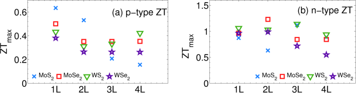
Figure Electronic and Thermoelectric Properties of Few-Layer Transition Metal Dichalcogenides summarizes the values from the PBE calculations for the peak n-type and p-type ZT and power factors for each TMDC material and layer thickness. In the n-type MoSe2, WS2 and WSe2 structures, the peak power-factor and the peak ZT do not occur at the same film thickness. For example, in MoSe2, a single monolayer has the highest power factor, and a bilayer has the highest ZT. This can be explained by the increase in the electronic thermal conductivity, as the Fermi level is moved into the conduction band.
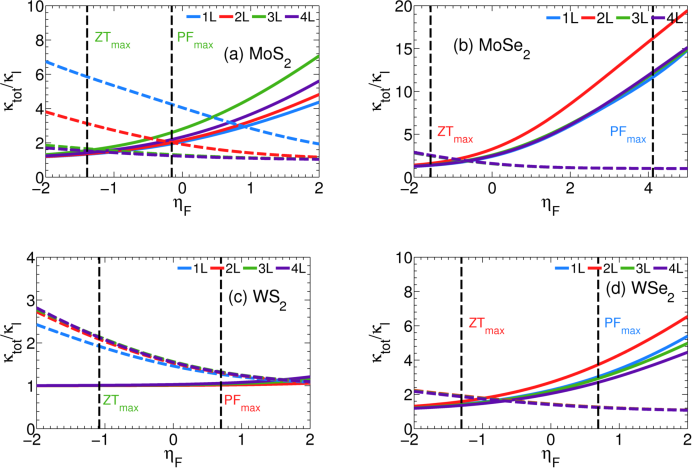
Figure Electronic and Thermoelectric Properties of Few-Layer Transition Metal Dichalcogenides shows the ratio of the total thermal conductivity, , with respect to the lattice thermal conductivity, , for each TMDC material. The two guide lines on each figure illustrate the reduced Fermi level position at which the maximum n-type power factor and ZT occurs. The ratio is higher at the Fermi level position where the the maximum power factor occurs. This increase in explains why the peak power factor and ZT occur at different Fermi energies and film thicknesses.
A number of recent studies report on the theoretical Li et al. (2013); Cai et al. (2014) and experimental values Muratore et al. (2013); Yan et al. (2014) of the lattice thermal conductivity on monolayer and few-layer TMDC materials with values of ranging from 19 Wm-1K-1 to 83 Wm-1K-1. Experimental measurements of the in-plane in suspended samples of MoS2 Yan et al. (2014) find a value of 34.5 Wm-1K-1 for 1L MoS2 and 52 Wm-1K-1 for few-layer MoS2. To assess whether the inequivalent values for the monolayer and few-layer TMDC films leave the predicted thermoelectric trends unchanged, we computed the thermoelectric parameters using =34.5 Wm-1K-1 for the monolayer and =52 Wm-1K-1 for the few-layer TMDC films of each material. The values of ZT differ compared to using =19 Wm-1K-1 for each film thickness. For MoS2, the room temperature n-type ZT values using the thickness dependent (constant) for the 1L, 2L, 3L and 4L structures are 0.87 (1.35), 0.63 (1.15), 1.11 (2.23), 0.89 (1.78). The maximum n-type ZT still occurs for the 3L structure and the minimum n-type ZT still occurs for the 1L structure. The trends for all of the n-type materials are preserved when a thickness dependent thermal conductivity is used. All of the values are shown in Fig. Electronic and Thermoelectric Properties of Few-Layer Transition Metal Dichalcogenides(b). For the n-type materials, changes in the density of modes are the dominant factor determining the trends. For p-type MoSe2, WS2, WSe2, ZT varies little for different layer thicknesses when using a constant as shown in Fig. Electronic and Thermoelectric Properties of Few-Layer Transition Metal Dichalcogenides(a). For p-type MoS2, the difference between the maximum ZT of a bilayer and the second highest value of a monolayer is small. Therefore, reducing the value of for a monolayer from 52 to 35.4 WM-1K-1 is sufficient to cause the peak value of ZT to occur at monolayer thickness for all 4 p-type materials as shown in Fig. Electronic and Thermoelectric Properties of Few-Layer Transition Metal Dichalcogenides(a).
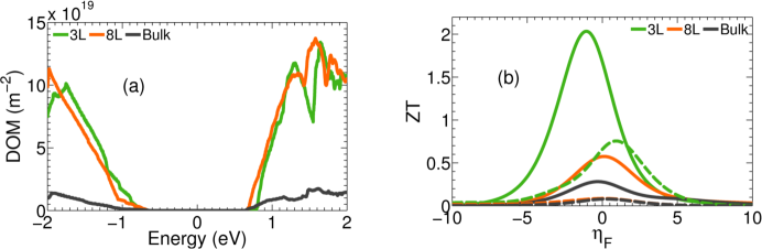
In an attempt to study the transition of the thermoelectric performance from few-layer films to bulk like performance, we calculate the thermoelectric parameters for an 8L film of WS2. Figure Electronic and Thermoelectric Properties of Few-Layer Transition Metal Dichalcogenides illustrates the density of modes and the ZT for bulk, 3L and 8L WS2. The n-type 0.974 ZT value of the 8L film is a factor of 1.9 smaller than that of the 4L film, but it is still a factor of 3.5 larger than that of the bulk. The p-type 0.163 ZT value of the 8L film is a factor of 4.7 smaller than that of the 4L film, and it is a factor of 2.0 larger that that of the bulk. Even at 8 monolayers, there is still an enhancement of the ZT value compared to that of the bulk, and the enhancement is larger in the n-type material.
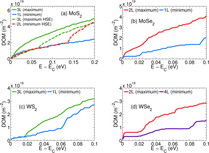
The thermoelectric performance in the low dimensional structures is enhanced by the more abrupt step-like shape of the density of modes distribution.Kim et al. (2009) It is clear from Eq. (4), that with , a step-function density of modes removes all negative contributions to the integrand of giving a maximum value for . The conduction band DOM distribution for the maximum and minimum ZT structures for each material are plotted in Figure Electronic and Thermoelectric Properties of Few-Layer Transition Metal Dichalcogenides. In all cases, the DOM with the sharper turn-on at the band edge gives rise the the maximum value for ZT.
IV DISCUSSION
The enhancement in the thermoelectric performance of few monolayer TMDC materials is in contrast to the enhanced thermoelectric performance observed for only a single quintuple (QL) layer of p-type Bi2Te3. Above 1 QL of Bi2Te3, the thermoelectric figure of merit approaches the bulk ZT. Zahid and Lake (2010); Maassen and Lundstrom (2013). The enhancement of ZT in n-type monolayer Bi2Te3 is minimal. This difference in the effect of layer thickness on ZT in the two different classes of materials can be explained by differences in the effect of thickness on the band-edge degeneracy and the density of modes. The valence band of monolayer Bi2Te3 is a ring in k-space that covers much of the Brillouin zone as shown in Fig. 4(d) of Ref. Maassen and Lundstrom, 2013. Thus, the integration over in Eq. (7) jumps from zero in the band gap to a finite number at the band edge resulting in a step-function turn-on of the valence band density of modes as seen in Fig. 3 of Ref. Zahid and Lake, 2010 and Fig. 2 of Ref. Maassen and Lundstrom, 2013. The size of the ring in k-space quickly collapses for thicknesses above a monolayer, and the large enhancement in ZT dissappears. In a parabolic band, the band edge is a point in k-space, and, in two-dimensions, the density of modes turns on smoothly as .Kim et al. (2009) The band edge of n-type monolayer Bi2Te3 remains parabolic resulting in a smooth turn-on of the density-of-modes and no significant enhancement of ZT.
The bands of the TMDC materials also remain parabolic at the band edges, however the conduction bands at the and the valleys become nearly degenerate for few monolayer thicknesses as shown in Fig. Electronic and Thermoelectric Properties of Few-Layer Transition Metal Dichalcogenides. Since the valley is 6-fold degenerate, and the valley is 3-fold degenerate, this results in a near 9-fold degeneracy of the conduction band edge. This increases the density of modes in the conduction band by a factor of 9 from that of a single valley. Furthermore, with increasing film thickness from 1L to 4L, the splitting of the bands resulting from interlayer coupling is on the order of . In MoS2, the splitting at is 0.4 meV for the 2L and 40 meV for the 4L structure. The other materials show similar magnitudes of the energy splitting as a function of thickness. Therefore, the near-degeneracy of the bands at increases linearly with the film thickness, so that the number of modes per layer becomes relatively insensitive to the layer thickness for few monolayer thicknesses.
The interlayer coupling of the out-of-plane d and pz orbitals result in the strongest interlayer hybridization and energy level splitting.Komsa and Krasheninnikov (2013) In MoS2 the orbital composition of the conduction band valley is 36 d, 22 dxy, 23 d, 6% pz, and 5% px and py. The d-orbital composition of the valley is 67% d. With increasing layer number, the valley splitting is larger than so that the number of modes contributed by the valleys remains 3 independent of layer number. Thus, when the valley falls within of the valley, its contribution to the density of modes dominates for few-layer thicknesses. Beyond 4 layers, the total splitting becomes larger than , and the number of accessible modes at no longer increases linearly with thickness.
Beyond a monolayer, the valence band shifts to for MoS2, MoSe2 and WS2. The energy difference between and varies as a function of the film thickness and material. For MoS2 the energy difference between and increases from 35 meV for the bilayer to 470 meV and 510 meV for the 3L and 4L structures respectively. The near degeneracy of the and valleys leads to the largest p-type density of modes for 2L MoS2. For MoSe2, the and valleys are nearly degenerate above a single monolayer. In WS2, the energy difference of the and valleys decreases from 42 meV to 21 meV as the film thickness is increased from a bilayer to four layers. For WSe2, the valence band maxima continues to reside at beyond a monolayer. Once the valence band valleys begin to contribute in MoSe2, WS2, and WSe2, the density of modes per layer becomes relatively independent of layer thickness, since there is little splitting of the valleys due to the interlayer coupling.Komsa and Krasheninnikov (2013) The valley orbital composition contains no d or components. In MoS2, the splitting varies from 0.2 meV for the 2L structure to 7.6 meV for the 4L structure. The other materials show similar magnitudes of the energy splitting as a function of thickness. Thus, at room temperature, the number of contributed modes per layer within of the valley minimum remains constant for thicknesses in the range of one to four monolayers.
For the 8 layer WS2 structure, the conduction band and valleys are still nearly degenerate. The valley lies 21 meV above the valley. However, at both valleys, the total splitting of the 8 bands contributed from the 8 layers is much greater than at room temperature. At , only two of the 8 bands are within 26 meV of the valley minimum. The overall energy splitting of the 8 bands at is 193 meV. In the valence band, the valley is 22 meV below the valley. However, the 8 bands from the 8 monolayers are split over a total range of 180 meV, and the second band is 40 meV below the valley maximum. Thus, as the number of layers increase, the total energy splitting of the bands contributed from each layer increases, and the number of modes per layer within of the valley minimums decreases.
As the number of layers becomes macroscopic such that the crystal is periodic in all three dimensions, the total splitting of the bands evolves into the width of the dispersive band along for the bulk crystal. For bulk WS2, the width of the band along the vertial direction from to at the top of the Brillouin zone is 208 meV which is 15 meV larger than the total splitting of the 8 layer stack. Furthermore, in the bulk, the valley is 126 meV above the minimum, so the contributes no modes to the density of modes near the conduction band edge. In the valence band, the valley maximum is 225 meV below the maximum, so that the density of modes near the valence band edge, is entirely from the valley. The lack of valley near-degeneracy and the width of the bulk dispersive bands along , result in a minimum density of modes per layer near the band edges compared to those of few layer structures. The reduced number of modes per layer within of the band edges results in reduced per-layer values of the thermoelectric figure of merit.
For both material systems Bi2Te3 and the semiconducting TMDCs, the enhancement of ZT results from the increased degeneracy or near-degeneracy of the band edges. The origin and nature of the degeneracy is different. In the Bi2Te3, the valence band edge becomes inverted into a ring as a result of the coupling of the topological surface states. In the TMDCs at few-layer thicknesses, different valleys become nearly degenerate. In the conduction band, the valleys become nearly degenerate with the valleys, and they contribute 6 more modes to the 3 modes from the valleys. In the valence band, the valleys become nearly degenerate with the , and they contribute 3 more modes. Furthermore, because of the weak interlayer coupling at and , the additional bands from additional layers lie within of the band edges for few layers. The increased band-edge degeneracy results in a sharper turn-on of the density of modes and an increased value of ZT.
V SUMMARY
The electronic structure of one to four monolayers of the semiconducting transition metal dichalcogenides MoS2, MoSe2, WS2 WSe2 are calculated using DFT with spin-orbit coupling and the PBE functional. Comparisons are made to results in the absence of spin-orbit coupling, and the PBE results are compared to HSE calculations for MoS2. The peak n-type value of ZT increases by a factor of over the bulk value for all materials. Among the 4 materials and 4 thicknesses, bilayer MoSe2 gives the maximum n-type ZT value of 2.4. The peak p-type value of ZT increases by a factor of over the bulk value for all materials. The maximum p-type ZT value of 1.2 occurs for bilayer MoS2. The maximum power factor generally occurs for a different layer thickness and at a more degenerate Fermi level than the maximum value of ZT. This difference can be explained by the increased electrical thermal conductivity at the Fermi level corresponding to the maximum power factor. For all materials, the maximum value of ZT coincides with the sharpest turn-on of the density of modes distribution at the band edge. The sharper turn-on is driven by the near valley degeneracy of the conduction band and valleys and the valence band and valleys. For few layer structures, the degeneracy is enhanced by the weak interlayer coupling at the and valleys.
Acknowledgements.
This work is supported in part by the National Science Foundation (NSF) Grant Nos. 1124733 and 1128304 and the Semiconductor Research Corporation (SRC) Nanoelectronic Research Initiative as a part of the Nanoelectronics for 2020 and Beyond (NEB-2020) program, FAME, one of six centers of STARnet, a Semiconductor Research Corporation program sponsored by MARCO and DARPA, and the University Grant Council (Contract No. AoE/P-04/08) of the Government of HKSA (FZ). This work used the Extreme Science and Engineering Discovery Environment (XSEDE), which is supported by National Science Foundation grant number OCI-1053575.References
- Radisavljevic et al. (2011) B. Radisavljevic, A. Radenovic, J. Brivio, V. Giacometti, and A. Kis, Nature Nanotechnology 6, 147 (2011), URL http://www.nature.com/nnano/journal/v6/n3/abs/nnano.2010.279.html.
- Yoon et al. (2011) Y. Yoon, K. Ganapathi, and S. Salahuddin, Nano Letters 11, 3768 (2011), eprint http://pubs.acs.org/doi/pdf/10.1021/nl2018178, URL http://pubs.acs.org/doi/abs/10.1021/nl2018178.
- Fang et al. (2012) H. Fang, S. Chuang, T. C. Chang, K. Takei, T. Takahashi, and A. Javey, Nano Letters 12, 3788 (2012).
- Alam and Lake (2012) K. Alam and R. K. Lake, IEEE Trans. Electron Devices 59, 3250 (2012).
- Han Liu and Ye (2012) A. N. Han Liu and P. Ye, ACS Nano 6, 8563 (2012).
- Li and Galli (2007) T. Li and G. Galli, The Journal of Physical Chemistry C 111, 16192 (2007), eprint http://pubs.acs.org/doi/pdf/10.1021/jp075424v, URL http://pubs.acs.org/doi/abs/10.1021/jp075424v.
- Xiao et al. (2012) D. Xiao, G.-B. Liu, W. Feng, X. Xu, and W. Yao, Phys. Rev. Lett. 108, 196802 (2012), URL http://link.aps.org/doi/10.1103/PhysRevLett.108.196802.
- Novoselov and Neto (2012) K. S. Novoselov and A. H. C. Neto, Physica Scripta 2012, 014006 (2012), URL http://stacks.iop.org/1402-4896/2012/i=T146/a=014006.
- Wang et al. (2012) Q. H. Wang, K. Kalantar-Zadeh, A. Kis, J. N. Coleman, and M. S. Strano, Nature Nanotech. 7, 699 (2012).
- Geim and Grigorieva (2013) A. Geim and I. Grigorieva, Nature 499, 419 (2013), URL http://www.nature.com/nature/journal/v499/n7459/abs/nature12385.html.
- Xu et al. (2013) M. Xu, T. Liang, M. Shi, and H. Chen, Chemical Reviews 113, 3766 (2013), eprint http://pubs.acs.org/doi/pdf/10.1021/cr300263a, URL http://pubs.acs.org/doi/abs/10.1021/cr300263a.
- Butler et al. (2013) S. Z. Butler, S. M. Hollen, L. Cao, Y. Cui, J. A. Gupta, H. R. Gutirrez, T. F. Heinz, S. S. Hong, J. Huang, A. F. Ismach, et al., ACS Nano 7, 2898 (2013), eprint http://pubs.acs.org/doi/pdf/10.1021/nn400280c, URL http://pubs.acs.org/doi/abs/10.1021/nn400280c.
- Sun et al. (2012) Y. Sun, H. Cheng, S. Gao, Q. Liu, Z. Sun, C. Xiao, C. Wu, S. Wei, and Y. Xie, Journal of the American Chemical Society 134, 20294 (2012), eprint http://pubs.acs.org/doi/pdf/10.1021/ja3102049, URL http://pubs.acs.org/doi/abs/10.1021/ja3102049.
- Goyal et al. (2010) V. Goyal, D. Teweldebrhan, and A. A. Balandin, Applied Physics Letters 97, 133117 (pages 3) (2010), URL http://link.aip.org/link/?APL/97/133117/1.
- Ghaemi et al. (2010) P. Ghaemi, R. S. K. Mong, and J. E. Moore, Phys. Rev. Lett. 105, 166603 (2010), URL http://link.aps.org/doi/10.1103/PhysRevLett.105.166603.
- Zahid and Lake (2010) F. Zahid and R. Lake, Applied Physics Letters 97, 212102 (pages 3) (2010), URL http://link.aip.org/link/?APL/97/212102/1.
- Maassen and Lundstrom (2013) J. Maassen and M. Lundstrom, Applied Physics Letters 102, 093103 (pages 4) (2013), URL http://link.aip.org/link/?APL/102/093103/1.
- (18) F.Zahid and R.K.Lake, Unpublished.
- Amara et al. (1987) A. Amara, Y. Frongillo, M. J. Aubin, S. Jandl, J. M. Lopez-Castillo, and J. P. Jay-Gerin, Phys. Rev. B 36, 6415 (1987), URL http://link.aps.org/doi/10.1103/PhysRevB.36.6415.
- Imai et al. (2001) H. Imai, Y. Shimakawa, and Y. Kubo, Phys. Rev. B 64, 241104 (2001), URL http://link.aps.org/doi/10.1103/PhysRevB.64.241104.
- Guo et al. (2013) H. Guo, T. Yang, P. Tao, Y. Wang, and Z. Zhang, Journal of Applied Physics 113, 013709 (pages 7) (2013), URL http://link.aip.org/link/?JAP/113/013709/1.
- Buscema et al. (0) M. Buscema, M. Barkelid, V. Zwiller, H. S. J. van der Zant, G. A. Steele, and A. Castellanos-Gomez, Nano Letters 0, null (0), eprint http://pubs.acs.org/doi/pdf/10.1021/nl303321g, URL http://pubs.acs.org/doi/abs/10.1021/nl303321g.
- Huang et al. (2013) W. Huang, H. Da, and G. Liang, Journal of Applied Physics 113, 104304 (pages 7) (2013), URL http://link.aip.org/link/?JAP/113/104304/1.
- Lee et al. (2013) C. Lee, J. Hong, M.-H. Whangbo, and J. H. Shim, Chemistry of Materials 25, 3745 (2013), eprint http://pubs.acs.org/doi/pdf/10.1021/cm402281n, URL http://pubs.acs.org/doi/abs/10.1021/cm402281n.
- Blöchl (1994) P. E. Blöchl, Phys. Rev. B 50, 17953 (1994).
- Perdew et al. (1996) J. P. Perdew, K. Burke, and M. Ernzerhof, Phys. Rev. Lett. 77, 3865 (1996).
- Ernzerhof and Scuseria (1999) M. Ernzerhof and G. E. Scuseria, J. Chem. Phys. 110, 5029 (1999).
- Kresse and Hafner (1993) G. Kresse and J. Hafner, Phys. Rev. B 48, 13115 (1993).
- Kresse and Furthmuller (1996) G. Kresse and J. Furthmuller, Comput. Mater. Sci. 6, 15 (1996).
- Grimme (2006) S. Grimme, Journal of Computational Chemistry 27, 1787 (2006), ISSN 1096-987X, URL http://dx.doi.org/10.1002/jcc.20495.
- Heyd et al. (2003) J. Heyd, G. E. Scuseria, and M. Ernzerhof, The Journal of Chemical Physics 118, 8207 (2003), URL http://scitation.aip.org/content/aip/journal/jcp/118/18/10.1063/1.1564060.
- Jeong et al. (2010) C. Jeong, R. Kim, M. Luisier, S. Datta, and M. Lundstrom, Journal of Applied Physics 107, 023707 (pages 7) (2010), URL http://link.aip.org/link/?JAP/107/023707/1.
- Paul et al. (2012) A. Paul, S. Salamat, C. Jeong, G. Klimeck, and M. Lundstrom, Journal of Computational Electronics 11, 56 (2012), ISSN 1569-8025, URL http://dx.doi.org/10.1007/s10825-011-0379-2.
- Kim et al. (2009) R. Kim, S. Datta, and M. S. Lundstrom, Journal of Applied Physics 105, 034506 (pages 6) (2009), URL http://link.aip.org/link/?JAP/105/034506/1.
- Mansfield and Salam (1953) R. Mansfield and S. A. Salam, Proceedings of the Physical Society. Section B 66, 377 (1953), URL http://stacks.iop.org/0370-1301/66/i=5/a=305.
- Thakurta and Dutta (1983) S. Thakurta and A. Dutta, Journal of Physics and Chemistry of Solids 44, 407 (1983).
- Kaasbjerg et al. (2012) K. Kaasbjerg, K. S. Thygesen, and K. W. Jacobsen, Phys. Rev. B 85, 115317 (2012), URL http://link.aps.org/doi/10.1103/PhysRevB.85.115317.
- Varshney et al. (2010) V. Varshney, S. S. Patnaik, C. Muratore, A. K. Roy, A. A. Voevodin, and B. L. Farmer, Computational Materials Science 48, 101 (2010), ISSN 0927-0256, URL http://www.sciencedirect.com/science/article/pii/S0927025609004583.
- Chiritescu et al. (2007) C. Chiritescu, D. G. Cahill, N. Nguyen, D. Johnson, A. Bodapati, P. Keblinski, and P. Zschack, Science 315, 351 (2007).
- Bronsema et al. (2004) K. Bronsema, J. De Boer, and F. Jellinek, Zeitschrift fur anorganische und allgemeine Chemie 540, 15 (2004).
- Schutte et al. (1987) W. Schutte, J. D. Boer, and F. Jellinek, Journal of Solid State Chemistry 70, 207 (1987), URL http://www.sciencedirect.com/science/article/pii/0022459687900570.
- Kam and Parkinson (1982) K. K. Kam and B. A. Parkinson, The Journal of Physical Chemistry 86, 463 (1982), eprint http://pubs.acs.org/doi/pdf/10.1021/j100393a010, URL http://pubs.acs.org/doi/abs/10.1021/j100393a010.
- Jiang (2012) H. Jiang, The Journal of Physical Chemistry C 116, 7664 (2012), eprint http://pubs.acs.org/doi/pdf/10.1021/jp300079d, URL http://pubs.acs.org/doi/abs/10.1021/jp300079d.
- Coehoorn et al. (1987) R. Coehoorn, C. Haas, J. Dijkstra, C. J. F. Flipse, R. A. de Groot, and A. Wold, Phys. Rev. B 35, 6195 (1987), URL http://link.aps.org/doi/10.1103/PhysRevB.35.6195.
- Ding et al. (2011a) Y. Ding, Y. Wang, J. Ni, L. Shi, S. Shi, and W. Tang, Physica B: Condensed Matter 406, 2254 (2011a), ISSN 0921-4526, URL http://www.sciencedirect.com/science/article/pii/S0921452611002651.
- Kuc et al. (2011a) A. Kuc, N. Zibouche, and T. Heine, Phys. Rev. B 83, 245213 (2011a), URL http://link.aps.org/doi/10.1103/PhysRevB.83.245213.
- Liu et al. (2011) L. Liu, S. Bala Kumar, Y. Ouyang, and J. Guo, Electron Devices, IEEE Transactions on 58, 3042 (2011), ISSN 0018-9383.
- Kuc et al. (2011b) A. Kuc, N. Zibouche, and T. Heine, Phys. Rev. B 83, 245213 (2011b).
- Ding et al. (2011b) Y. Ding, Y. Wang, J. Ni, L. Shi, S. Shi, and W. Tang, Physica B: Condensed Matter 406, 2254 (2011b), URL http://www.sciencedirect.com/science/article/pii/S092145261100265.
- Ramasubramaniam (2012) A. Ramasubramaniam, Phys. Rev. B 86, 115409 (2012), URL http://link.aps.org/doi/10.1103/PhysRevB.86.115409.
- Mak et al. (2010) K. F. Mak, C. Lee, J. Hone, J. Shan, and T. F. Heinz, Phys. Rev. Lett. 105, 136805 (2010), URL http://link.aps.org/doi/10.1103/PhysRevLett.105.136805.
- Cheiwchanchamnangij and Lambrecht (2012) T. Cheiwchanchamnangij and W. R. Lambrecht, Phys. Rev. B 85, 205302 (2012), URL http://link.aps.org/doi/10.1103/PhysRevB.85.205302.
- Shi et al. (2013) H. Shi, H. Pan, Y.-W. Zhang, and B. I. Yakobson, Phys. Rev. B 87, 155304 (2013), URL http://link.aps.org/doi/10.1103/PhysRevB.87.155304.
- Zahid et al. (2013a) F. Zahid, L. Liu, Y. Zhu, J. Wang, and H. Guo, AIP Advances 3, 052111 (pages 6) (2013a), URL http://link.aip.org/link/?ADV/3/052111/1.
- Pichanusakorn and Bandaru (2009) P. Pichanusakorn and P. R. Bandaru, Applied Physics Letters 94, (2009), URL http://scitation.aip.org/content/aip/journal/apl/94/22/10.1063/1.3147186.
- Zahid et al. (2013b) F. Zahid, L. Liu, Y. Zhu, J. Wang, and H. Guo, AIP Advances 3, 052111 (pages 6) (2013b), URL http://link.aip.org/link/?ADV/3/052111/1.
- Li et al. (2013) W. Li, J. Carrete, and N. Mingo, Applied Physics Letters 103, 253103 (2013), URL http://scitation.aip.org/content/aip/journal/apl/103/25/10.1063/1.4850995.
- Cai et al. (2014) Y. Cai, J. Lan, G. Zhang, and Y.-W. Zhang, Phys. Rev. B 89, 035438 (2014), URL http://link.aps.org/doi/10.1103/PhysRevB.89.035438.
- Muratore et al. (2013) C. Muratore, V. Varshney, J. J. Gengler, J. J. Hu, J. E. Bultman, T. M. Smith, P. J. Shamberger, B. Qiu, X. Ruan, A. K. Roy, et al., Applied Physics Letters 102, 081604 (2013), URL http://scitation.aip.org/content/aip/journal/apl/102/8/10.1063/1.4793203.
- Yan et al. (2014) R. Yan, J. R. Simpson, S. Bertolazzi, J. Brivio, M. Watson, X. Wu, A. Kis, T. Luo, A. R. Hight Walker, and H. G. Xing, ACS Nano 8, 986 (2014), eprint http://pubs.acs.org/doi/pdf/10.1021/nn405826k, URL http://pubs.acs.org/doi/abs/10.1021/nn405826k.
- Komsa and Krasheninnikov (2013) H.-P. Komsa and A. V. Krasheninnikov, Phys. Rev. B 88, 085318 (2013).
- Zeng et al. (2013) H. Zeng, G.-B. Liu, J. Dai, Y. Yan, B. Zhu, R. He, L. Xu, S. Xu, X. Chen, and X. Cui, Nature Scientific Reports 3 (2013).


| () | () | ) | ) | (eV) | (eV) | |||
|---|---|---|---|---|---|---|---|---|
| MoS2 | 3.179 | 12.729 | 0.627 | 3.160 | 12.290 | 0.629 | 1.060 | 1.29 |
| MoSe2 | 3.309 | 13.323 | 0.624 | 3.289 | 12.927 | 0.621 | 0.959 | 1.09 |
| WS2 | 3.183 | 13.131 | 0.630 | 3.150 | 12.320 | 0.622 | 1.283 | 1.35 |
| WSe2 | 3.319 | 13.729 | 0.627 | 3.282 | 12.960 | 0.621 | 1.188 | 1.20 |
| Structure | Point | MoS2 | MoSe2 | WS2 | WSe2 | MoS2 | MoSe2 | WS2 | WSe2 |
|---|---|---|---|---|---|---|---|---|---|
| Hole Effective Mass (m0) | Electron Effective Mass (m0) | ||||||||
| 1L | Kl | 0.543 | 0.578 | 0.339 | 0.341 | 0.506 | 0.502 | 0.349 | 0.345 |
| Kt | 0.546 | 0.588 | 0.339 | 0.348 | 0.504 | 0.503 | 0.347 | 0.345 | |
| 2L | 1.039 | 1.430 | 1.239 | 1.322 | - | - | - | - | |
| Kl | 0.548 | 0.595 | 0.345 | 0.349 | 0.521 | 0.539 | 0.359 | 0.411 | |
| Kt | 0.546 | 0.596 | 0.346 | 0.348 | 0.510 | 0.539 | 0.359 | 0.412 | |
| 3L | 1.239 | 1.432 | 1.246 | 1.382 | - | - | - | - | |
| Kt | 0.549 | 0.602 | 0.366 | 0.368 | 0.559 | 0.544 | 0.376 | 0.434 | |
| Kt | 0.548 | 0.604 | 0.366 | 0.368 | 0.559 | 0.544 | 0.377 | 0.434 | |
| 4L | 1.239 | 1.433 | 1.351 | 1.432 | - | - | - | - | |
| Kl | 0.548 | 0.604 | 0.366 | 0.367 | 0.554 | 0.542 | 0.376 | 0.435 | |
| Kt | 0.546 | 0.604 | 0.366 | 0.368 | 0.559 | 0.549 | 0.377 | 0.434 | |
| Bulk | 0.838 | 0.973 | 0.832 | 0.997 | - | - | - | - | |
| - | - | - | - | 0.590 | 0.521 | 0.569 | 0.489 | ||
| - | - | - | - | 0.845 | 0.776 | 0.665 | 0.643 | ||
| Structure | Transition | MoS2 | MoSe2 | WS2 | WSe2 | MoS2 | MoSe2 | WS2 | WSe2 |
|---|---|---|---|---|---|---|---|---|---|
| Calculated (eV) | Experimental (eV) | ||||||||
| 1L | to Kc | 1.705 | 1.768 | 1.849 | 1.776 | - | - | - | - |
| to | 1.922 | 1.862 | 1.929 | 1.806 | - | - | - | - | |
| Kv1 to Kc | 1.600 | 1.375 | 1.573 | 1.254 | 1.900 | 1.660 | 1.950 | 1.640 | |
| Kv2 to Kc | 1.750 | 1.556 | 1.973 | 1.715 | 2.050 | 1.850 | 2.360 | 2.040 | |
| 2L | to Kc | 1.564 | 1.368 | 1.507 | 1.586 | 1.600 | - | 1.730 | - |
| to | 1.775 | 1.373 | 1.542 | 1.562 | - | - | - | - | |
| Kv1 to Kc | 1.600 | 1.373 | 1.549 | 1.269 | 1.880 | - | 1.910 | 1.590 | |
| Kv2 to Kc | 1.760 | 1.556 | 1.977 | 1.788 | 2.050 | - | 2.340 | 2.000 | |
| 3L | to Kc | 1.150 | 1.334 | 1.458 | 1.586 | - | - | - | - |
| to | 1.171 | 1.372 | 1.482 | 1.508 | - | - | - | - | |
| Kv1 to Kc | 1.620 | 1.376 | 1.485 | 1.265 | - | - | - | - | |
| Kv2 to Kc | 1.780 | 1.564 | 1.873 | 1.783 | - | - | - | - | |
| 4L | to Kc | 1.120 | 1.351 | 1.438 | 1.546 | - | - | - | - |
| to | 1.139 | 1.374 | 1.439 | 1.434 | - | - | - | - | |
| Kv1 to Kc | 1.630 | 1.356 | 1.459 | 1.259 | - | - | - | - | |
| Kv2 to Kc | 1.780 | 1.574 | 1.877 | 1.753 | - | - | - | - | |
| Bulk | to | 1.060 | 0.959 | 1.283 | 1.188 | 1.290 | 1.090 | 1.350 | 1.200 |
| Kv1 to Kc | 1.590 | 1.349 | 1.453 | 1.258 | 1.880 | 1.350 | 1.880 | 1.580 | |
| Kv2 to Kc | 1.780 | 1.588 | 1.889 | 1.737 | 2.060 | 1.380 | 2.320 | 1.950 | |
NOTE: The band gap of 2L, 3L and 4L WSe2 occurs between the Kv1 and . The 2L, 3L and 4L band gaps of WSe2 are 1.216 eV, 1.1594 eV and 1.1345 eV respectively.
| Temperature | 1L | 2L | 3L | 4L | Bulk | |
|---|---|---|---|---|---|---|
| Maximum n-type (p-type) Power Factor () | ||||||
| MoS2 | 300K | .130 (.150) | .140 (.110) | .280 (.041) | .220 (.031) | .0320 (.010) |
| 150K | .093 (.072) | .093 (.071) | .190 (.032) | .120 (.024) | .012 (.0042) | |
| 77K | .072 (.043) | .072 (.053) | .13 (.021) | .063 (.022) | .012 (.0031) | |
| MoSe2 | 300K | .340 (.071) | .330 (.094) | .230 (.082) | .230 (.071) | .022 (.0061) |
| 150K | .151 (.050) | .200 (.051) | .100 (.051) | .100 (.052) | .013 (.004) | |
| 77K | .062 (.031) | .120 (.032) | .062 (.031) | .052 (.032) | .013 (.0032) | |
| WS2 | 300K | .240 (.062) | .280 (.061) | .270 (.071) | .240 (.092) | .022 (.0052) |
| 150K | .110 (.042) | .160 (.042) | .150 (.041) | .130 (.051) | .010 (.0043) | |
| 77K | .051 (.031) | .081 (.032) | .070 (.032) | .081 (.031) | .010 (.0022) | |
| WSe2 | 300K | .260 (.054) | .240 (.052) | .190 (.053) | .160 (.053) | .022 (.014) |
| 150K | .141 (.030) | .140 (.031) | .081 (.031) | .070 (.031) | .010 (.004) | |
| 77K | .071 (.031) | .082 (.031) | .050 (.031) | .043 (.022) | .011 (0.0021) | |
| Temperature | 1L | 2L | 3L | 4L | Bulk | |
|---|---|---|---|---|---|---|
| Maximum n-type (p-type) ZT | ||||||
| MoS2 | 300K | 1.35 (.970) | 1.35 (1.15) | 2.23 (.510) | 1.78 (.390) | .350 (.081) |
| 150K | .590 (.350) | .590 (.450) | 1.03 (.220) | .660 (.160) | .110 (.034) | |
| 77K | .240 (.140) | .240 (.190) | .420 (.093) | .210 (.062) | .031 (.012) | |
| MoSe2 | 300K | 1.39 (.800) | 2.39 (.810) | 1.66 (.810) | 1.65 (.810) | .290 (.081) |
| 150K | .450 (.310) | 1.06 (.320) | .610 (.320) | .570 (.320) | .100 (.033) | |
| 77K | .130 (.120) | .410 (.120) | .220 (.120) | .170 (.120) | .030 (.014) | |
| WS2 | 300K | 1.52 (.70) | 1.98 (.720) | 2.03 (.760) | 1.85 (.760) | .280 (.082) |
| 150K | .411 (.280) | .613 (.280) | .770 (.280) | .721 (.350) | .104 (.030) | |
| 77K | .120 (.110) | .181 (.113) | .211 (.113) | .271 (.113) | .034 (.012) | |
| WSe2 | 300K | 1.88 (.620) | 1.92 (.620) | 1.44 (.620) | 1.13 (.620) | .260 (.120) |
| 150K | .590 (.220) | .750 (.220) | .490 (.220) | .380 (.220) | .091 (.032) | |
| 77K | .180 (.100) | .270 (.100) | .170 (.100) | .130 (.100) | .031 (.014) | |