The Crystal and Electronic Structures of Cd3As2, the 3D Electronic Analogue to Graphene
Abstract
The structure of Cd3As2, a high mobility semimetal reported to host electrons that act as Dirac particles, is reinvestigated by single crystal X-ray diffraction. It is found to be centrosymmetric rather than noncentrosymmetric as previously reported. It has a distorted superstructure of the antifluorite (M2X) structure type with a tetragonal unit cell of a = 12.633(3) and c = 25.427(7) Å in the centrosymmetric I41/acd space group. The antifluorite superstructure can be envisioned as consisting of distorted Cd62 cubes (where = an empty cube vertex) in parallel columns, stacked with opposing chirality. Electronic structure calculations performed using the experimentally determined centrosymmetric structure are similar to those performed with the inversion symmetry absent, but with the important implication that Cd3As2 is a 3D-Dirac semimetal with no spin splitting; all bands are spin degenerate and there is a four-fold degenerate bulk Dirac point at the Fermi Energy along -Z in the Brillouin zone. This makes Cd3As2 a 3D electronic analog to graphene. Scanning Tunneling Microscopy experiments identify a 2x2 surface reconstruction in the (112) cleavage plane of single crystals; needle crystals grow with a [110] long axis direction.
1 Introduction
The topology-dependent electronic properties of solids are the subject of considerable current research. Although theoretical and experimental exploration of the electronic implications of topology fall clearly in the realm of materials physics 1, the compounds of interest for displaying those properties have a well-defined set of chemical characteristics, including constituent elements with similar electronegativities and strong spin orbit coupling; crystal symmetry also plays a critical role 2. The fact that such properties are in many cases predictable by theory has generated a wide interest in finding compounds that display them. Although the edges and surfaces of crystals and extremely thin crystals such as graphene might reasonably be expected to display electronic properties dependent on their topology König02112007, 3, 4, there are also cases where topological properties have been predicted for electrons within bulk three dimensional crystals 5, 6. Such is the case for the recently emergent compounds Na3Bi and Cd3As2, where early characterization of the real materials indicates that this may indeed be the case 7, 8, 9. One important prediction within this category is that in some cases the electrons will behave like they obey the “Weyl Hamiltonian”, a previously unobserved electronic state 10, 11. In this instance the presence or absence of a center of symmetry in the host crystal is a critical structural characteristic for the stability of the electronic phase.
Cd3As2 has been well studied in the past 12, 13, 14 but not in this context. Of particular interest have been its semimetallic character and very high electron mobility 13. It is also of interest for solar cells and as an analog for graphene in exploratory device applications 15, 16. Theoretical work on the electronic structure of Cd3As2 has been done, but the calculations were performed using either the primitive tetragonal (P42/nmc) intermediate temperature structure (475 - 600 )17 or the noncentrosymmetric low temperature (Below 475 ) structure18(I41cd) proposed by Steigmann and Goodyear 19. The primitive tetragonal structure (1935) (a = 8.95 Å, c = 12.65 Å) has As in a FCC array, with 6 Cd in fluorite-like positions - 2 of the 8 vertices of the distorted cube are fully empty. The empty vertices lie diagonally opposite each other in one face of the cube, and are ordered in a two-dimensional array. The low temperature structure (1968) has a larger unit cell (a = 12.67 Å, c = 25.48 Å) where the empty cube vertices order in a three-dimensional rather than a two-dimensional array. Recent theoretical calculations performed with the reported non-centrosymmetric low temperature I41cd structure 19 indicate that Cd3As2 may be a new type of 3D-Dirac semi-metal in part due to the lack of inversion symmetry, which causes the lifting of the spin degeneracy of certain bands in the vicinity of the Dirac point, raising the possibility that Cd3As2 may be an example of a Weyl semimetal. Thus the presence or absence of inversion symmetry has important implications for the electronic properties of Cd3As2.
Here we re-examine the crystal structure of Cd3As2 using current single crystal X-ray diffraction (SXRD) and analysis methods. We also identify the growth direction of needle crystals and the cleavage plane as the [110] and (112), respectively. Through the use of Scanning Tunneling Microscopy (STM) experiments, we identify a 2x2 surface reconstruction of the (112) plane cleavage surface. We find that earlier researchers failed to appreciate the near centrosymmetricity of their reported structure, and that Cd3As2 in its low temperature phase is in fact centrosymmetric, with the space group I41/acd. The higher symmetry forbids any spin splitting and keeps all bands at least two fold degenerate; this has significant implications for the behavior of the electrons near the Fermi Energy. The inversion symmetry constrains Cd3As2 to be a non-spin-polarized 3D-Dirac semi-metal, and therefore implies that it is a 3D analog to graphene, where the electronic states are also non-spin-polarized.
2 Experimental
Silvery, metallic colored single crystals of Cd3As2 were grown out of a Cd-rich melt with the stoichiometry (Cd5)Cd3As2. The elements were sealed in an evacuated quartz ampoule, heated to 825 , and kept there for 48 hours. The sample was then cooled at a rate of 6 degrees per hour to 425 and was subsequently centrifuged. Only Cd3As2 crystals were formed, with a crystal to flux ratio of 1:5, consistent with the equilibrium phase diagram 20. Chemical analysis of the crystals was performed in an FEI Quanta 200 FEG Environmental-SEM by energy dispersive x-ray analysis (EDX), which found them to have a Cd:As ratio of 1.500(1):1. Powder X-ray diffraction (PXRD) patterns were collected using Cu K radiation on a Bruker D8 Focus diffractometer with a graphite monochromator on ground single crystals to confirm the identity of the compound as being Cd3As2 in the low temperature structure. The single crystal X-ray diffraction study was performed on a 0.04 mm x 0.04 mm x 0.4 mm crystal on a Bruker APEX II diffractometer using Mo K radiation ( = 0.71073 Å) at 100 K. Exposure time was 35 seconds with a detector distance of 60 mm. Unit cell refinement and data integration were performed with Bruker APEX2 software. A total of 1464 frames were collected over a total exposure time of 14.5 hours. 21702 diffracted peak observations were made, yielding 1264 unique observed reflections (centrosymmetric scaling) collected over a full sphere. No diffuse scattering was observed. The crystal structure was refined using the full-matrix least-squares method on F2, using SHELXL2013 implemented through WinGX. An absorption correction was applied using the analytical method of De Meulenaer and Tompa 21 implemented through the Bruker APEX II software. The crystal surfaces were studied with in a home-built cryogenic scanning tunneling microscope at 2 K. No twinning was observed in either the STM or single crystal diffraction measurements. Electronic structure calculations were performed in the framework of density functional theory using the Wien2k code22 with a full-potential linearized augmented plane-wave and local orbitals basis together with the Perdew-Burke-Ernzerhof parameterization of the generalized gradient approximation23. The plane wave cutoff parameter RMTKmax was set to 7 and the Brillouin zone (BZ) was sampled by 250 k-points. The experimentally determined structure was used and spin orbit coupling (SOC) was included.
3 Results and Discussion
3.1 X-ray Diffraction
From SXRD, a body-centered tetragonal unit cell of a = 12.633(3) and c = 25.427(7) was found, matching PXRD measurements. The systematic absences of the reflections in the SXRD reciprocal lattice are consistent with the possible space groups I41cd and I41/acd as previously described 18. It has previously been theorized that Cd3As2 has the ideal Mn7SiO12 structure type in the I41/acd space group, 24 but no experimentally determined atomic positions were reported. Here, initial refinements in setting 2 of the centrosymmetric space group I41/acd were performed with all atoms on the idealized positions of the Mn7SiO12 structure type. This idealized model gave very poor fits to the data, with R1 only falling to 60. It was clear from analysis of the electron density maps that the atoms are in fact not at the ideal positions. In the final refinement, atomic positions as well as anisotropic thermal parameters for all atoms were allowed to vary freely. The refinement results are summarized in Table 1. Table 2 lists final positions for all atoms and Table 3 lists the Cd-As bond lengths. Refined atomic displacement parameters may be found in the .cif file.
| Phase | Cd3As2 |
|---|---|
| Symmetry | Tetragonal, I41/acd (No. 142) |
| Cell Parameters (Å) | a = b = 12.633(3), c = 25.427(7) |
| = = = 90∘ | |
| Wavelength (Å) | Mo K - 0.71073 |
| Temperature (K) | 100 |
| V (Å3) | 4058.0(2) |
| Z | 32 |
| Calculated Density (g/cm3) | 6.38 |
| Formula Weight (g/mol) | 487.1 |
| Absorption Coefficient (mm-1) | 25.07 |
| Observations | 21702 |
| F000 | 6720 |
| Data/Restraints/Parameters | 1264/0/48 |
| R1 (all reflections) | 0.0480 |
| R1 Fo 4(Fo) | 0.0220 (893) |
| wR2 (all) | 0.040 (1264) |
| Rint/R() | 0.0617/0.0238 |
| Difference e- density (e/Å3) | 1.24/-1.25 |
| GooF | 1.035 |
Resolving the ambiguity between a centrosymmetric crystal structure and a noncentrosymmetric crystal structure that is nearly centrosymmetric can sometimes be difficult, and is a well-known problem in crystallography25, 26. Unless a clear choice can be made in favor of the noncentrosymmetric model, structures must be described centrosymmetrically25. The authors of the previous non-centrosymmetric structure report did not appreciate the fact that an alternative origin choice would allow for a centrosymmetric structure and thus did not check a centrosymmetric model against their observed intensities, which were estimated from exposed film densities 18. In order to compare a noncentrosymmetric model for Cd3As2 to the centrosymmetric model, we carried out a refinement in the noncentrosymmetric I41cd space group, using the published model as a template. The final refinements (see supplementary information) with atomic positions and anisotropic displacement parameters allowed to vary yielded a wR2 of 0.0489 for 2481 data (with noncentrosymmetric scaling) with 93 parameters and an R1 = 0.0265 for 1639 Fo 4F. The centrosymmetric model displays significantly better R-values. The R1 value for example for all data for the I41/acd solution is 0.0481 while for the I41cd solution it is 0.0611. This is an improvement by a factor of 1.22 for the centrosymmetric structure. In addition, we used PLATON27 to check for and detect missed symmetry28. The ADDSYM analysis (Le Page algorithm for missing symmetry) was used on the previously reported I41cd noncentrosymmetric structure. For that noncentrosymmetric model, PLATON detected a missing inversion center at (0, ) in the unit cell and recommended a 180∘ rotation around the c-axis followed by an origin shift to (0, -, ), and a suggested space group of I41/acd. Further, the deviations of the atoms in the noncentrosymmetric model from their equivalents in the centrosymmetric model are calculated and found to be very small (.03 Å, supplementary info). Finally the Flack parameter (supplementary info) indicated that the structure was not noncentrosymmetric 29. This analysis thus further confirmed that the centrosymmetric crystal structure is the correct one.
3.2 Crystal Structure
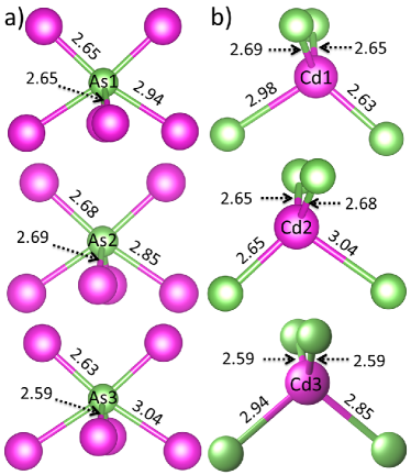
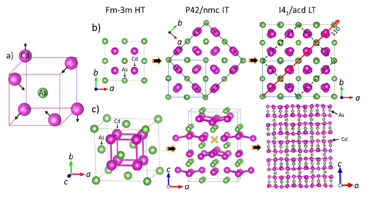
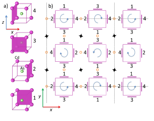
Cd3As2 has different but related crystal structures as a function of temperature, which all can be considered defect antifluorite types; the Cd is distributed in the cube-shaped array occupied by F in CaF2, while the As is in the FCC positions that are occupied by Ca. Thus in Cd3As2, the formally Cd2+ ions are four-coordinated by As and the formally As3- ions are eight-coordinated by Cd. With As3- in VI fold coordination expected to have a radius of about 2.22 Å and Cd2+ in IV coordination expected to have a radius of about 0.92 Å, the , which is near the ideal 0.414 cutoff for tetrahedral coordination of the metal in the CaF2-type structure ( = 0.15 - 0.414).30. Further, as evidenced by the stoichiometry, Cd3As2 is Cd deficient of the ideal Cd4As2 antifluorite formula, missing of the Cd atoms needed to form a simple cube around the As. Thus the (distorted) cube can be written as Cd62, where = an empty vertex. The As and Cd coordinations in our Cd3As2 structure are shown in Figure 1. In the ordered, lower temperature variants, the Cd atoms shift from the ideal antifluorite positions toward the empty vertices of the cube (shown in Figure 2a). This distortion makes occupancy of the empty vertices highly energetically unfavored. At high temperatures (T 600 ) the Cd ions are disordered31 and so Cd3As2 adopts the ideal antifluorite space group Fm-3m with a = 6.24 Å (The HT structure). Between 600 and 475 , the intermediate temperature (IT) P42/nmc structure is found, where the Cd ions order so that the empty vertices are located on diagonally opposite corners of one face of the Cd62 cubes (see below). These cubes then stack so that the empty vertices form channels parallel to the a and b axes at different levels along the c axis31. On further cooling, another ordering scheme is found. Below 475 , the Cd atoms further order in a three-dimensional fashion, such that each distorted Cd62 cube stacks on top of the previous one after a 90∘ rotation (either clockwise or counter-clockwise depending on the particular chain) about the stacking axis (parallel to the c axis). This is the low temperature (LT) centrosymmetric I41/acd structure of the crystals whose structure is determined here and whose physical properties are of current interest. This also appears to be a new structure type. Figures 2b and 2c show how the three structures are related: the P42/nmc structure is a supercell of the disordered Fm-3m structure, and the I41/acd structure is a supercell of the P42/nmc structure.
| Atom | Wyckoff | x | y | z |
| Cd1 | 32g | 0.13955(3) | 0.36951(3) | 0.05246(2) |
| Cd2 | 32g | 0.11162(3) | 0.64230(3) | 0.07243(2) |
| Cd3 | 32g | 0.11863(3) | 0.10598(4) | 0.06247(2) |
| As1 | 32g | 0.24602(4) | 0.25779(5) | 0.12315(2) |
| As2 | 16d | 0 | 0.99931(2) | |
| As3 | 16e | 0.51070(7) | 0 |
| Atom1 | Atom2 | Distance Å | Atom1 | Atom2 | Distance Å | |
|---|---|---|---|---|---|---|
| As1 | Cd3 | 2.6250(8) | Cd1 | As3 | 2.6282(8) | |
| Cd2 | 2.6507(8) | As1 | 2.6518(8) | |||
| Cd1 | 2.6518(8) | As2 | 2.6858(7) | |||
| Cd2 | 2.6552(8) | As1 | 2.9838(8) | |||
| Cd3 | 2.9408(8) | |||||
| Cd1 | 2.9837(8) | |||||
| As2 | Cd2 | 2.6771(8) | Cd2 | As1 | 2.6507(8) | |
| Cd2 | 2.6771(8) | As1 | 2.6552(8) | |||
| Cd1 | 2.6858(7) | As2 | 2.6771(8) | |||
| Cd1 | 2.6858(7) | As3 | 3.0351(8) | |||
| Cd3 | 2.8522(7) | |||||
| Cd3 | 2.8522(7) | |||||
| As3 | Cd3 | 2.5935(7) | Cd3 | As3 | 2.5935(7) | |
| Cd3 | 2.5935(7) | As1 | 2.6250(8) | |||
| Cd1 | 2.6282(8) | As2 | 2.8522(7) | |||
| Cd1 | 2.6282(8) | As1 | 2.9408(8) | |||
| Cd2 | 3.0351(8) | |||||
| Cd2 | 3.0351(8) |
The I41/acd structure has 3 unique Cd atoms and 3 unique As atoms and is schematically shown in Figure 3. Since the empty vertices of the Cd62 cubes sit diagonally opposite each other in a face of the distorted cube, the incomplete Cd cube can be thought of as having only one “closed face”. This “closed face” changes position in either a clockwise or counter-clockwise fashion as the cubes stack along the c direction, resulting in a screwing chain of cubes. These chains then align so that each chain is next to a chain of an opposite handedness; a right-handed chain is surrounded by left-handed chains. This results in an inversion center being present between each chain.
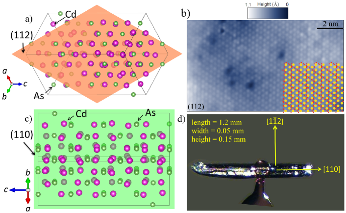
For physical property measurements, it is important to identify characteristic planes and directions in the as-grown crystals. Cd3As2 grown as described here forms both irregular and rod-like crystals, all of which appear to have planar pseudo-hexagonal surfaces, often in steps, perpendicular to the long crystal axis. While the detailed SXRD measurements for structural refinement were carried out on small crystals, which gave the cleanest diffraction spots, larger crystals are employed for property measurements. Several of these larger crystals (e.g. with typical dimensions of 0.15 mm by 0.05 mm by 1.2 mm) were used in order to ascertain the growth direction of the needles. The crystals were mounted onto flat kapton holders and the Bruker APEX II software32 was used to indicate the face normals of the crystal after the unit cell and orientation matrix were determined. The largest crystals were also placed onto PXRD slides and oriented diffraction experiments were conducted. The long axis of the needles was consistently found to be the [110] direction. The planar pseudo-hexagonal crystal surfaces with normals perpendicular to the growth direction are the (112) planes; these correspond to the close packed planes in the cubic antifluorite phase transformed into the LT structure supercell Miller indices. STM studies find that the cleavage plane of Cd3As2 is the pseudo-hexagonal (112) plane found here as a well-developed face in the bulk crystals. Figure 4a shows a projection of the structure with the (112) plane shaded in orange. Figure 4b is a topographic STM image (V -250 mV, I = 50 pA, Temp = 2 K) of the (112) cleavage plane. The nearest neighbor spacing is found to 4.40.1 Å, which is consistent with the As-As spacing or Cd-Cd spacing on a (112) type plane. Also visible in the inset of Figure 4b is the appearance of a 2x2 surface reconstruction, likely due to dangling bonds from the termination of the (112) plane during cleavage. Figure 4c is a projection slightly off of the [110] direction, with the corresponding lattice plane shaded in green. Figure 4d shows the unit cell axes and the growth directions of a large needle crystal of Cd3As2 that is suitable for physical property measurements.
A [110] needle direction for a tetragonal symmetry crystal is relatively uncommon 33. The crystal growth conditions employed in this study were such that the majority of the slow cooling took place through the stable temperature region of the IT P42/nmc structure. We hypothesize that the fastest growing direction in this phase is along the chain axis of the empty cube vertices, which is a principal axis of the structure (either the a or b axis). Thus the needle crystals have already grown before the last 50 degrees of the cooling, during which the low temperature annealing results in the ordering of the Cd atoms that yields the I41/acd structure. As can be seen from Figure 2, the principal axes of the P42/nmc structure become the set of [110] directions in the I41/acd structure. Variation of the growth temperature and conditions in future crystal growth studies may result in different types of needle axes, but the (112) close packed plane for crystal face development and cleavage is likely to be strongly preferred.
3.3 Electronic Structure
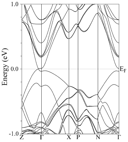
The electronic structure calculated from the experimentally determined centrosymmetric structure found here (Table 2) is shown in Figure 5. This band structure is similar to that reported previously for the incorrect noncentrosymmetric crystal structure19. Crucially, however, due to the inversion symmetry present in the I41/acd structure, there is no spin splitting around the Dirac point (where the bands cross between and Z at EF and all bands are at least two-fold degenerate. Thus, the centrosymmetric structure indicates that Cd3As2 is a 3D-Dirac semi-metal with two fold degenerate bands that come together to a four-fold degenerate Dirac point at the Fermi level. It is therefore the 3D analog to graphene, where there is also no spin-splitting at the Dirac point. Furthermore, the states at the point can now be characterized by their full symmetry (including their inversion eigenvalue) thus allowing parity counting to demonstrate the nontrivial topology in this ground state.
4 Conclusion
In conclusion, we report the correct crystal structure of Cd3As2 in the low temperature, three-dimensionally ordered phase, as well as the corresponding electronic structure. We identify that for crystals grown as reported here, the needle growth direction is the [110] and the cleavage plane and most developed face in crystals is the pseudo-hexagonal (112) plane. Also present is a 2x2 surface reconstruction of the (112) plane cleavage surface. We found that Cd3As2 crystallizes in the centrosymmetric, I41/acd space group, and as such appears to be a new structure type. The Cd62 cubes order in a spiral, corkscrew fashion along an axis parallel to c. Each corkscrew is surrounded by corkscrews of the opposite handedness, which results in the overall structure having inversion symmetry. The previously reported model in the I41cd space group (# 110), where an inversion center was omitted, can be related to this structure by rotating by 180∘ about the c-axis and then shifting the origin to 0, -, . Since the correct centrosymmetric structural model uses only 6 unique atoms to describe the structure, electronic structure calculations become much more facile, which will help with the theoretical analysis of the electronic structure of this phase. In electronic structure calculations based on the centrosymmetric crystal structure, we find that the previously reported bulk band crossing along -Z at the Fermi level is maintained, however due to the inversion symmetry, no spin splitting is allowed. Therefore Cd3As2 is expected to be a non-spin-split 3D-Dirac semi-metal, and a three-dimensional analog to graphene.
{acknowledgement}
This research was supported by the Army Research Office, grant W911NF-12-1-0461.
References
- Hasan and Kane 2010 Hasan, M. Z.; Kane, C. L. Rev. Mod. Phys. 2010, 82, 3045–3067
- Cava et al. 2013 Cava, R. J.; Ji, H.; Fuccillo, M. K.; Gibson, Q. D.; Hor, Y. S. J. Mater. Chem. C 2013, 1, 3176–3189
- Hasan and Moore 2011 Hasan, M. Z.; Moore, J. E. Annual Review of Condensed Matter Physics 2011, 2, 55–78
- Novoselov et al. 2005 Novoselov, K.; Geim, A. K.; Morozov, S.; Jiang, D.; Grigorieva, M. K. I.; Dubonos, S.; Firsov, A. Nature 2005, 438, 197–200
- Young et al. 2012 Young, S. M.; Zaheer, S.; Teo, J. C. Y.; Kane, C. L.; Mele, E. J.; Rappe, A. M. Phys. Rev. Lett. 2012, 108, 140405
- Xu et al. 2011 Xu, G.; Weng, H.; Wang, Z.; Dai, X.; Fang, Z. Phys. Rev. Lett. 2011, 107, 186806
- Borisenko et al. 2013 Borisenko, S.; Gibson, Q.; Evtushinsky, D.; Zabolotnyy, V.; Buechner, B.; Cava, R. J. arXiv preprint arXiv:1309.7978 2013,
- Neupane et al. 2013 Neupane, M.; Xu, S.; Sankar, R.; Alidoust, N.; Bian, G.; Liu, C.; Belopolski, I.; Chang, T.-R.; Jeng, H.-T.; Lin, H.; Bansil, A.; Chou, F.; Hasan, M. Z. arXiv preprint arXiv:1309.7892 2013,
- Liu et al. 2014 Liu, Z. K.; Zhou, B.; Zhang, Y.; Wang, Z. J.; Weng, H. M.; Prabhakaran, D.; Mo, S.-K.; Shen, Z. X.; Fang, Z.; Dai, X.; Hussain, Z.; Chen, Y. L. Science 2014,
- Wan et al. 2011 Wan, X.; Turner, A. M.; Vishwanath, A.; Savrasov, S. Y. Phys. Rev. B 2011, 83, 205101
- Balents 2011 Balents, L. Physics 2011, 4, 36
- Lin-Chung 1969 Lin-Chung, P. Physical Review 1969, 188, 1272–1280
- Rosenberg and Harman 1959 Rosenberg, A. J.; Harman, T. C. Journal of Applied Physics 1959, 30, 1621–1622
- Wallace 1979 Wallace, P. Physica Status Solidi (b) 1979, 92, 49–55
- Saraswat et al. 2006 Saraswat, K.; Chui, C. O.; Kim, D.; Krishnamohan, T.; Pethe, A. High Mobility Materials and Novel Device Structures for High Performance Nanoscale MOSFETs. 2006
- Stoumpos et al. 2013 Stoumpos, C. C.; Malliakas, C. D.; Kanatzidis, M. G. Inorganic Chemistry 2013, 52, 9019–9038
- Stackelberg and Paulus 1935 Stackelberg, M.; Paulus, R. Z. Physik. Chem. 1935, 28B, 427
- Steigmann and Goodyear 1968 Steigmann, G.; Goodyear, J. Acta Crystallographica Section B: Structural Crystallography and Crystal Chemistry 1968, 24, 1062–1067
- Wang et al. 2013 Wang, Z.; Weng, H.; Wu, Q.; Dai, X.; Fang, Z. Phys. Rev. B 2013, 88, 125427
- Cahn 1991 Cahn, R. W. Advanced Materials 1991, 3, 628–629
- de Meulenaer and Tompa 1965 de Meulenaer, J.; Tompa, H. Acta Crystallographica 1965, 19, 1014–1018
- Blaha et al. 1990 Blaha, P.; Schwarz, K.; Sorantin, P.; Trickey, S. Computer Physics Communications 1990, 59, 399–415
- Perdew et al. 1996 Perdew, J. P.; Burke, K.; Ernzerhof, M. Physical Review Letters 1996, 77, 3865
- Zdanowicz et al. 1964 Zdanowicz, W.; Lukaszewicz, K.; Trzebiatowski, W. Bulletin de l’Academi Polonaise des Sciences, Serie des Sciences Chimiques 1964, 12, 169–176
- Marsh 1986 Marsh, R. E. Acta Crystallographica Section B 1986, 42, 193–198
- Ermer and Dunitz 1970 Ermer, O.; Dunitz, J. D. Acta Crystallographica Section A 1970, 26, 163
- Spek 2009 Spek, A. L. Acta Crystallographica Section D: Biological Crystallography 2009, 65, 148–155
- Flack et al. 2006 Flack, H.; Bernardinelli, G.; Clemente, D.; Linden, A.; Spek, A. Acta Crystallographica Section B: Structural Science 2006, 62, 695–701
- Flack 1983 Flack, H. D. Acta Crystallographica Section A 1983, 39, 876–881
- Müller 1993 Müller, U. Inorganic Structural Chemistry; New York, 1993
- Pietraszko and Lukaszewicz 1982 Pietraszko, A.; Lukaszewicz, K. Acta Crystallographica Section B: Structural Science 1982, 25, 988–990
- Bruker 2013 Bruker, APEX II; Bruker AXS Inc Madison, Wisconsin, USA, 2013
- Buerger 1956 Buerger, M. Elementary Crystallography: An Introduction to the Fundamental Geometrical Features of Crystals; Wiley, 1956; pp 134–142
Synopsis
![[Uncaptioned image]](/html/1312.7576/assets/x6.png)
The structure of Cd3As2, a high mobility semimetal reported to host electrons that act as Dirac particles, is reinvestigated by single crystal X-ray diffraction. It is found to be centrosymmetric rather than noncentrosymmetric as previously reported. It has a distorted superstructure of the antifluorite (M2X) structure type with a tetragonal unit cell of a = 12.633(3) and c = 25.427(7) Å in the centrosymmetric I41/acd space group. Electronic structure calculations performed using the experimentally determined centrosymmetric structure are similar to those performed with the inversion symmetry absent, but with the important implication that Cd3As2 is a 3D-Dirac semimetal with no spin splitting; there is a four-fold degenerate bulk Dirac point at the Fermi Energy along -Z in the Brillouin zone. This makes Cd3As2 a 3D electronic analog to graphene.