Electron transport in quantum wire superlattices
Abstract
Electronic transport is theoretically investigated in laterally confined semiconductor superlattices using the formalism of non-equilibrium Green’s functions. Velocity-field characteristics are calculated for nanowire superlattices of varying diameters, from the quantum dot superlattice regime to the quantum well superlattice regime. Scattering processes due to electron-phonon couplings, phonon anharmonicity, charged impurities, surface and interface roughness and alloy disorder are included on a microscopic basis. Elastic scattering mechanisms are treated in a partial coherent way beyond the self-consistent Born approximation. The nature of transport along the superlattice is shown to depend dramatically on the lateral dimensionality. In the quantum wire regime, the electron velocity-field characteristics are predicted to deviate strongly from the standard Esaki-Tsu form. The standard peak of negative differential velocity is shifted to lower electric fields, while additional current peaks appear due to integer and fractional resonances with optical phonons.
I Introduction
Electron transport in superlattices (SLs) has been widely studied in the case of 1D periodic arrangement of 2D semiconductor layers Esaki and Tsu (1970); Sibille et al. (1990); Wacker (2002) (Fig. 1a). In contrast, the nature of charge transport in superlattices of lower dimensionality remains an open question. The nature and efficiency of dissipative processes are well known to strongly depend on the dimensionality, with longest lifetimes and coherence times in 3D quantum confined structures Bockelmann and Bastard (1990); Benisty et al. (1991); Zibik et al. (2009); Grange (2009). Quantum dot (QD) SLs are hence expected to display radically different non-equilibrium transport properties than quantum well (QW) SLs. Potential applications for high performance thermoelectric convertersLin and Dresselhaus (2003), photovoltaicsNozik (2002), and quantum cascade lasersWingreen and Stafford (1997); Grange (2013) further motivates the fundamental understanding of the non-equilibrium transport properties of SLs with 3D quantum confinement.
Though ballistic transport in a QW SL is ideally a pure 1D problem, scattering processes couples all spatial degrees of freedom (Fig. 1a). In QW SLs, the in-plane free electron motion possesses a continuous dispersion. During the scattering processes, energy transfer occurs between the axial and lateral motions. Hence the effective energy conservation laws in the motion along the SL axis can greatly differ from the 3D one of the involved scattering mechanisms. For example, in QW heterostructures, 3D elastic scattering processes due to static defects act effectively as 1D inelastic scattering mechanisms with respect to the motion along the SL. In contrast, in the limit of purely 1D SL with 0D lateral motion (Fig. 1d), the lateral state is frozen so that the 3D energy conservation laws of the scattering processes apply directly to the 1D motion along the SL.
The effect of dissipation on 1D quantum electron transport has been investigated in finite quantum region such as atomic wiresFrederiksen et al. (2007) and stacked QDs Gnodtke et al. (2006). Quantum dissipative transport in QD SLs has been studied in Ref. Vukmirovic et al., 2007 for high electric fields. However full velocity-field characteristics of 1D SLs have not been calculated so far. In particular it is still unkown how the Esaki-Tsu negative differential velocity (NDV) Esaki and Tsu (1970) evolves when the lateral dimensionality is reduced towards QD SLs.

In this article, we present a detailed theory of electron transport in semiconductor SLs laterally confined in nanowires using the framework of non-equilibrium Green’s functions (NEGF). The formalism presented here allows to describe the transport in SLs for any lateral dimensionality from the regime of coupled 0D QDs (Fig. 1d) to the one of coupled 2D QWs (Fig. 1a). For this purpose, we include in our modeling the scattering mechanisms that are known to be important in planar QW heterostructures as well as the ones specific to quasi-0D systems. Specifically, we consider the mechanism of anharmonic polaron decay which has been shown to be dominant in InGaAs self-assembled QDs Grange et al. (2007); Zibik et al. (2009). In addition, as the nature of elastic scattering mechanisms evolves from incoherent to coherent as the dimensionality decreases, we include a coherent treatment of elastic scattering processes for lateral state-conserving processes. The electronic transport properties are shown to depend dramatically on the SL lateral dimensionality. With increasing lateral confinement, the drift velocity-voltage characteristics evolve from the Esaki-Tsu form for usual QW SL, dominated by a single NDV effect, towards richer characteristics where (i) the linear conductivity increases, (ii) the standard Esaki-Tsu NDV occurs at much lower voltages, and (iii) large peaks due to integer and fractional resonances with optical phonons appear.
II Theory
Our aim is to model the non-equilibrium electron transport in a nanowire SL heterostructure. We first introduce the general form of the Hamiltonian. We then introduce an electronic basis set, and present the NEGF formalism. We then treat the relevant scattering terms arising from electron-phonon interactions and static disorder effects. Finally we present the method used for solving the self-consistent NEGF equations.
II.1 Hamiltonian of the nanowire superlattice
We consider charge carriers in a nanowire SL in interaction with phonon modes. The following Hamiltonian is used to model the system:
| (1) |
where is the electronic Hamiltonian of a single charge carrier in the idealized heterostructure under a homogeneous electric field (the length gauge will be used throughout this paper); is the static electronic potential due to disorder effects such as interface and surface roughness, charged impurities and alloy disorder; represents the interaction terms between electrons and phonons; is the vibrational Hamiltonian of the crystal, including its anharmonic part; represents the mean-field potential arising from the Coulomb interaction with other charge carriers. The standard caret notation is used to refer to operators.
II.2 Electronic structure and basis states
We consider cylindrical nanowires of diameter having SL heterostructures along their longitudinal axis. We use cylindrical coordinates () where is the nanowire axis (see Fig. 1b). The material composition and modeling parameters are assumed to depend only on the coordinate. The electronic structure is modeled considering a single band within the envelope function approximation. We consider a basis set of the form:
| (2) |
where the are defined below and are eigenstates of the Schrödinger equation on a homogeneous disk (i.e. the assumed nanowire cross-section):
| (3) |
where is the Bessel function of order and is its th zero. The indexes and are chosen such that they are associated with the th eigenvalue of the 2D lateral motion at the coordinate:
| (4) |
where is the material-dependent effective mass. For each lateral mode we are then left with a -dependent electronic Hamiltonian:
| (5) |
where is the electric field applied along the axis and
| (6) |
with being the material-dependent band-offset potential. The eigenstates of the periodic Hamiltonian satisfy the Bloch theorem and can be classified by wavevector and miniband index
| (7) |
In order to discretize the basis set in the direction, various choices are possible. A full real-space discretizationLake et al. (1997); Kubis et al. (2009) by e.g. finite differences requires a large basis size in order to quantitatively describe the miniband structure, rendering the NEGF numerical implementation challenging. On the other hand, mode-space approaches are also possible, and allow the description of the transport properties with a much smaller basis Lee and Wacker (2002); Lee et al. (2006); Vukmirovic et al. (2007). Here, the Hilbert space is reduced by keeping only a finite number of minibands, i.e. the low lying states of the unbiased structure. An energy cut-off is fixed and only the minibands separated from the ground state by less than are kept. Formally we define the following projection operator
| (8) |
In the following, the non-equilibrium dynamics will be computed within the subspace generated by . The various operators defined on the full Hilbert space need to be transformed in operators acting within the subspace. The restrictions of the unperturbed Hamiltonian and position operator are simply defined by:
| (9) |
| (10) |
Within the subspace, we consider the localized basis which is constructed by diagonalizing the position operator Lee et al. (2006); Vukmirovic et al. (2007):
| (11) |
where the () are sorted by increasing eigenvalues. In addition, their phase is chosen in order to fullfill periodicity:
| (12) |
where is an integer, is the number of minibands and is the period length.
All the terms in the Hamiltonian other than are functions of the sole operator. In order to conserve the commutation relation , i.e. to conserve their local nature, we use the following transformation:
| (13) |
This transformation allows us to keep exactly the same form for the current operator 111 In the work of Lee and coworkers Lee and Wacker (2002); Lee et al. (2006), an implicit truncation of the Hamiltonian leads instead to an additional current term which is found to be numerically negligible. :
| (14) |
We also keep only a finite number of lateral states satisfying . In the following NEGF simulations, it will be checked that the cut-off value is chosen high enough so that adding higher minibands and/or higher lateral states does not change significantly the calculated current. In the following, we will use exclusively operators acting in the subspace and all the subscripts indicating restricted operators will be omitted for simplicity.
II.3 Non-equilibrium Green’s functions
II.3.1 Electron Green’s functions
The NEGF formalism is generally introduced in terms of four Green’s functions (GFs) Datta (1997); Haug and Jauho (2008); Caroli et al. (1971); Mahan (1987). Here the lesser, upper, retarded and advanced electron GFs are defined respectively in terms of the following quantities:
| (15a) |
| (15b) |
| (15c) |
| (15d) |
where and are respectively the creation and annihilation operators in the electronic state . It is convenient to introduce the GF operators defined here by:
| (16) |
where refers to any of the four GFs. Since we do not consider spin-dependent effects, the spin index is not indicated here for simplicity and all quantities are implicitly spin diagonal. The spectral function reads in operator form:
| (17) |
The retarded GF can be expressed from the spectral function:
| (18) |
The lesser GF (15a) is an extension of the concept of density matrix for two different times. Its value at equal times corresponds to the density matrix:
| (19) |
Here, off-diagonal terms of the GFs are considered in the direction but not in the lateral directions where only the diagonal terms of the eigenmodes are considered. The calculations are thus independent of the basis choice along the -axis, allowing full coherent description of transport along the nanowire. In contrast, the use of only diagonal GF terms in the lateral directions does not allow us to describe coherent transport effects in the lateral directions. This seems a reasonable approximation for thin nanowires where the lateral scattering potentials are weak compared to the lateral quantization energies. On the other hand, in the limit of large diameter nanowire and planar heterostructures, this is equivalent to considering only GF terms which are diagonal in the in-plane momentum, similarly to previous implementations of NEGF in planar quantum well heterostructures Lake et al. (1997); Lee and Wacker (2002); Kubis et al. (2009). In this later case, lateral localization effects might become relevant at low temperature and/or in presence of strong disorder effects, which remains beyond the scope of this work.
In steady state, the GFs depend only on the time difference . In this case we will use one-time-dependent GFs . Energy-dependent GFs are then defined by Fourier-transforming these quantities
| (20) |
Moreover, in steady state, the advanced and retarded GFs are linked by
| (21) |
so that the GFs are forming only two independent quantities.
II.3.2 Phonon Green’s functions
The Hamiltonian of the vibration of the crystal reads
| (22) |
| (23) |
where and are respectively the harmonic and anharmonic parts, and and are the creation and annihilation operators for a phonon mode of branch with wavevector . The phonon GFs are defined byEconomou (1984):
| (24) |
| (25) |
| (26) |
with
| (27) |
In steady-state, we will use the same one-time notation and energy-dependent GFs as for electronic GFs (Eq. 20). When only the harmonic part of the Hamiltonian is taken into account, the lesser and retarded equilibrium phonon GFs for a mode of frequency read respectively:
| (28) |
| (29) |
where is the Bose factor at the energy . In the energy domain, it reads:
| (30) |
| (31) |
Harmonic phonon GFs are usually directly used in electron transport calculations. However, in this work, we will use instead anharmonic GFs for optical modes which will be derived below (Sec. II.6). This will allow us to account for the mechanism of anharmonic polaron decay.
II.4 Equations of motion
The equations of motion in the NEGF formalism can be expressed in terms of the so-called Dyson and Keldysh relations; in steady-state, they read respectively Datta (1997); Haug and Jauho (2008); Caroli et al. (1971); Mahan (1987):
| (32) |
| (33) |
where is the part of the interaction which is treated coherently. Here it reads , where is the mean-field Coulomb potential and is the part of the electronic disordered potential which is generated randomly and treated coherently (see below). Similarly to the spectral GF, the spectral self-energy is defined as
| (34) |
and the retarded self-energy can be expressed as:
| (35) |
In the energy domain, this relation reads:
| (36) |
where denotes the Hilbert tranform .
II.5 Self-energies due to electron-phonon interaction
We consider the interactions of electrons with longitudinal optical (LO), surface optical (SO) and longitudinal acoustic (LA) phonon modes laterally confined in the nanowire. Each interaction is of the form:
| (37) |
The form factors are given in appendix A for the different modes. In the self-consistent Born approximation (SCBA), the self-energies due to electron-phonon interaction are of the form:
| (38) |
Within the basis considered here, the nonvanishing coupling terms being diagonal with respect to the axial wavefunctions, the self-energy reads
| (39) |
where
| (40) |
II.5.1 Optical phonons
For longitudinal optical (LO) and surface optical (SO) phonons, we assume wavevector-independent optical phonon GFs. Indeed only long-wavelength optical phonons with negligible dispersion are effectively coupled to the relevant electronic states. We can then write
| (41) |
where
| (42) |
In the energy domain, it reads
| (43) |
If the phonon GF is taken harmonic, only quantized energy exchanges are allowed. In QDs, it has been shown that energy exchanges strongly differing from the optical phonon energy take place due to simultaneous electron-phonon interaction and anharmonic couplings among phonons Grange et al. (2007); Zibik et al. (2009). In these previous works, the electron-phonon interaction was diagonalized exactly, and the Fermi golden rule was used to calculate scattering rates among polaronic states induced by anharmonic couplings. Here, instead, the SCBA is used in order to treat the electron–optical-phonon interaction, and anharmonicity is included in the optical-phonon GFs. As already checked in Ref. Vukmirovic et al., 2007, the SCBA very well reproduces the exact polaron formation, especially for temperatures verifying where is the optical phonon energy. The calculation of anharmonic GFs is presented below.
II.5.2 Acoustic phonons
In contrast to optical phonons, the acoustic phonons are assumed to be harmonic and to have a linear dispersion. The corresponding self-energy can be expressed as:
| (44) |
where
| (45) |
II.6 Green’s functions of anharmonic phonons
We now calculate the anharmonic phonon GFs involved in the electron–optical-phonon self-energy. We retain only the cubic couplings in the anharmonic terms, and thermal equilibrium population of phonon modes is assumed. As we consider only diagonal terms in the phonon’s GFs, the Dyson equation reads
| (46) |
where is the phonon retarded self-energy. The lesser GF is then calculated using the Keldysh relation:
| (47) |
The phonon self-energy is calculated in the Born approximation, taking into account cubic anharmonic terms. The phonon lesser self-energy reads
| (48) |
in which we have taken the harmonic phonon GFs in the right hand side. The cubic anharmonic coupling is expressed in terms of the Grüneisen constant as reported in Ref. Grange et al., 2007. The phonon spectral and retarded self-energies are then given respectively by
| (49) |
| (50) |
where denotes the Hilbert transform. Applying the Dyson equation, we obtain the phonon lesser GF:
| (51) |
II.7 Elastic scattering
Disordered potentials due to randomly distributed charged impurities, alloy disorder, rough interfaces and rough surfaces break the ideal symmetry of the structure, and couple the dynamics in the various directions. In particular, they couple the 1D motion along the superlattice axis to the the lateral motion. In planar QW heterostructures, as the lateral dispersion forms a continuum, the static disorder produces an incoherent and irreversible evolution within the -electron basis. In contrast, in the limit of purely 1D heterostructures, where only one lateral state is involved, the evolution is completely reversible, as elastic couplings induce a unitary evolution within the -electron basis. A treatment of elastic scattering beyond the SCBA is thus required in these low-dimensional structures.
In previous studies, the surface roughness in nanowires has been treated coherently by random generation of surfacesWang et al. (2005); Lherbier et al. (2008). Here, we consider in addition interface roughness, impurity scattering and alloy scattering. Instead of generating microscopic random realizations of all surfaces, interfaces, charge positions, and alloy atom positions, we develop a simpler approach based on their correlations. We believe that it is sufficient for low or moderate disorder effects, which are anyway often not known precisely from the microscopic point of view. The disordered potentials are split into diagonal and off-diagonal parts with respect to the lateral eigenstates:
| (52) |
| (53) |
The diagonal component is treated coherently, while the off-diagonal part can only be treated incoherently since we consider only diagonal elements of the GFs with respect to the lateral states.
II.7.1 Elastic scattering self-energies
The off-diagonal elastic coupling component , which does not conserve the lateral state, is treated within the SCBA. The corresponding self-energy reads:
| (54) |
where
| (55) |
II.7.2 Elastic scattering coherent terms
In order to treat coherently the diagonal component , we first calculate the following covariance matrix
| (56) |
We then generate random potentials with correlations that obey this calculated covariance. To this purpose, we need to rotate the covariance matrix in its principal component basis. More precisely, the symmetric matrix can be diagonalized in
| (57) |
where is a diagonal matrix and is a unitary matrix. We then generate random diagonal matrices in the following way: for each diagonal element of index , we generate a random number obeying a Gaussian distribution with a variance . The random potential is then obtained by a back transformation into the original basis:
| (58) |
| (59) |
The potential is then included in in the Dyson equation (32) in order to be treated coherently. The all NEGF calculation is then made for different generated random potentials until the distribution of the calculated observables reached the desired accuracy.
II.8 Field-periodic boundary conditions
We assume the nanowire SL to contain an infinite number of periods of length . The possible formation of electrical field domains is not considered in this workEsaki and Chang (1974); Wacker (2002). Instead, the electric field is assumed to have the same periodicity as the SL. The field-periodic boundary condition for the mean-field component of the electrostatic potential reads
| (60) |
where is an arbitrary integer. Note that the externally applied electric field is already included in . The Poisson equation reads
| (61) |
where and are the charge densities of carriers and dopants respectively. From Eq. 61, this field-periodic boundary assumption implies that the electron probability distribution is periodic. In the length gauge used here, the periodicity condition for the GFs reads
| (62) |
where is the number of minibands. Note that in nanowires, the SL periodicity can be broken by the inclusion of the coherent disordered potentials (II.7.2). In order to investigate such effects, the simulated period can be increased to several SL periods. In this case, the period length in Eqs. 60 and 62 is replaced by where is the number of SL periods included in one computational period. In order to know the needed number of periods, the integer is increased until the calculated observables tend towards constant values.
II.9 Electron density and current
The expectation values of the various observables can be derived using the relation between the density matrix and the lesser GF at equal times (Eq. 19). The electron probability distribution is given by:
| (63) |
where the factor 2 arises from the spin index. Using the expression of the current operator in terms of the restricted operators (Eq. 13), the current reads
| (64) |
II.10 Numerical details
The self-consistent problem formed by the Keldysh equation, the Dyson relation, the expression of the various self-energies and the electrostatic Poisson equation is solved iteratively. Starting from an initial guess of the GFs, we calculate iteratively (i) the lesser and upper self-energies; (ii) the retarded self-energy (Eq. 36); (iii) the coherent part of the interaction, comprising the mean-field electrostatic potential and the random potential; (iv) the retarded GF from the Dyson equation; (v) the lesser GFs from the Keldysh relation. This procedure is repeated until a self-consistent solution is reached, with two convergence criteria based on both the lesser GF and the calculated current. Before each step (i), the GFs are renormalized in order to fulfill the charge neutrality for each period. It is checked that this renormalization factor converges accurately towards unity as the convergence is achieved.
The iterative steps (i) and (ii) are performed numerically in the time-domain. It is advantageous since the self-energies within the SCBA involves the product in the time domain. In contrast, energy domain calculations would involve numerically expensive convolutions, as a broad continuum of anharmonic optical phonons is considered. On the contrary, the iterative steps (iv) and (v) are more easily computed in the energy domain, so that Fourier transforms of the GFs and the self-energies are used respectively in between steps (v)-(i) and (ii)-(iv). Though adaptive energy grids have been shown to be useful in order to resolve GF peaks with a reduced number of energy pointsKubis et al. (2009), a homogeneous energy grid is used here in order to make use of a fast Fourier transform algorithm.
A maximum coherence length is set in the calculations, so that we consider only the GF terms for . Due to the field-periodic boundary conditions, the GFs are calculated for belonging to a given period, while varies away from within the set coherence length . In the simulation of the nanowire SL, we check that is taken large enough by increasing it until convergence of the calculated current. In the regime of QW SL, we have verified that there is no difference in the calculated observables considering one or several periods, provided the doping densities remain low enough to prevent the formation of field domain instabilities.
III Results and discussions
III.1 Transport in nanowire SLs: transition from QW to QD SLs


As an application of the theory presented above, we present calculations of the electronic transport in a GaAs/Al0.3Ga0.7As nanowire SL. One period consists in 5 nm GaAs (well) and 5 nm Al0.3Ga0.7As (barrier). The SL is assumed to be homogeneously n-doped with a concentration of cm-3. Assumed values for surface and interface roughnesses are given in appendix B. The fundamental subband has a width of meV. It is separated from the first excited subband by a minigap of meV. In the following calculations only the fundamental subband is considered (the cut-off value is taken around 100 meV). Fig. 2 shows the drift velocity as a function of the nanowire diameter for two different electric fields along the SL. For large nanowire diameters, the current density tends toward a constant value. This is interpreted as the 2D regime for the lateral motion. In contrast, for smaller diameters, the quantum wire regime is reached, and the current density varies with the lateral confinement. In order to confirm this interpretation, we plot in Fig. 3 the quantities
| (65) |
| (66) |
which represent respectively the spectral function and the electron density summed over the lateral states; is the nanowire cross-section and is the single basis state per period considered. For a nanowire diameter of 150 nm, the smooth shape of the spectral function indicates that the lateral quantization effects are overcome by broadening effects. Its flat shape is characteristic of a 2D subband. On the other hand, for nanowire diameters below 17 nm, the current displays relatively small variations in Fig. 2. This corresponds to a quasi-0D regime for the lateral motion, where only the ground lateral state is occupied, as shown in Fig. 3 for a nanowire diameter of 15 nm. In between these two limit regimes, large variations of the current densities are calculated in Fig. 2, corresponding to an intermediate dimensional regime where several but still distinct lateral states are involved, as depicted in Fig. 3 for nanowire diameters of 30 and 50 nm.
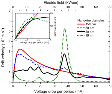
Fig. 4 shows the calculated velocity-voltage characteristics for various nanowire diameters. For a nanowire diameter of 150 nm, where the 2D lateral regime is reached in good approximation, the standard Esaki-Tsu behavior is observed: negative differential velocity (NDV) is expected to occur when the carriers are excited beyond an inflection point in the miniband dispersion Esaki and Tsu (1970). For smaller diameters, the characteristics deviate from this simple standard behavior. The most remarkable difference is the appearance of a large peak when the voltage drop per period matches the LO-phonon energy (=37 meV in GaAs). In addition, smaller resonances become visible at and . The interpretation is the following: in the 2D regime, the lateral motion acts as a continuous energy reservoir, which renders the 3D energy conservation laws of the scattering mechanisms not directly visible on the SL transport properties. In particular, though LO phonons provide the most efficient inelastic scattering processes, their quasi-monochromatic nature is not evidenced on the velocity–voltage characteristics. In contrast, in the limit of 1D SLs with 0D lateral motion, the energy is exchanged directly between the quantized SL levels (i.e. the Wannier-Stark states) and the phonons. Hence resonances in the transport occur when two consecutive Wannier-Stark levels are separated by the LO-phonon energy . The smaller resonances around and are attributed to LO-phonon assisted transport between states distant of 2 and 3 periods respectively.
In the inset of Fig. 4, we observe an increase in the electron mobility with decreasing NW thickness. This is attributed to the decrease of the efficiency of the scattering processes with decreasing dimensionality. In addition, the position of the first NDV peak shifts to smaller voltage values with decreasing NW thickness. This can be understood within the Esaki and Tsu semi-classical model Esaki and Tsu (1970), where the NDV peak is predicted to occur for ( being the scattering time). Beyond this critical point, the Esaki-Tsu model predicts that electrons are accelerated beyond an inflection point in the energy–momentum dispersion relation and hence experience a negative effective mass. This critical point can also be interpreted as the transition between the domain of validity of miniband transport and Wannier-Stark hopping models Wacker (2002). In both pictures, the overall reduction of scattering processes with decreasing dimensionality explains qualitatively the observed shift of the NDV peak towards lower voltages.
III.2 Role and nature of elastic scattering processes

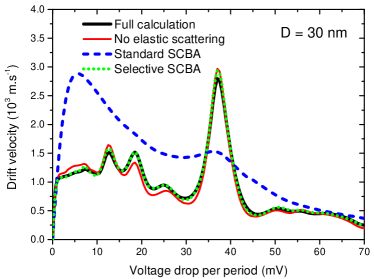

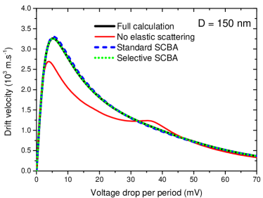
In order to analyze the role and the nature of elastic scattering processes, simulations with different treatments of elastic scattering are shown in Fig. 5. First, we discuss the comparison between full calculations with the one neglecting elastic scattering. These two calculations notably differ for thick NWs. In contrast, for thin NWs, the relative difference in the calculated transport is very small, indicating that elastic scattering only plays a minor role. This strong reduction of elastic scattering processes with decreasing dimensionality is consistent with the intuitive expectation that elastic mechanisms are suppressed by the discretization of energy levels.
Now we compare the calculations using the standard SCBA, the “selective SCBA” defined above and the full calculation. In the QW limit the standard SCBA, the “selective SCBA” and the full calculation are found to give the same results. In contrast, in the quantum wire regime, the standard SCBA totally differs from the two other models. The reason is that the standard SCBA fails when the fluctuations of the energy levels become larger than their linewidths. In contrast, in the present full calculation, the main coupling elements, which are diagonal with respect to the lateral eigenstates, are treated coherently. If we now compare the full calculation to the selective SCBA calculation, we can see that the selective SCBA provides an excellent approximation to the full calculation, down to 15 nm thin nanowires. Our interpretation is that the typical energy fluctuations of the levels stay smaller than the miniband width and are too weak to induce localization effects.
III.3 Role of phonon anharmonicity


In Fig. 6 we show a comparison of the calculations with and without the inclusion of phonon anharmonicity for various NW diameters. While the inclusion of anharmonicity is found to be almost irrelevant for thick NWs in the QW SL limit, striking differences are observed for thin NWs. Indeed the direct LO-phonon emission is gradually suppressed with decreasing dimensionality towards 0D systems, while the mechanism of anharmonic polaron decay becomes dominant. For very thin NW diameters corresponding to the pure 1D SL limit, note that the simulation without phonon anharmonicity does not converge due to the strong reduction of the linewidths below our numerical possibilities in energy resolution. Hence our calculations show a clear transition in the dominant energy dissipation pathway as the lateral dimensionality is reduced, from direct LO-phonon emission to polaron anharmonicity.
IV Conclusion
Within the NEGF formalism, we have developed a theory of electronic transport in nanowire SLs. This model allows the calculation of transport in a wide range of NW SL thickness, for lateral dimensionality ranging from 0D to 2D, i.e. from QD SL to QW SL. We have studied how the transport evolves with this change of lateral dimensionality. While velocity-voltage characteristics are dominated by the standard Esaki-Tsu NDV in QW SLs, electron-phonon resonances appear when the lateral quantum regime is reached. In addition, the electron mobility increases and the NDV peaks are strongly shifted to lower electric fields. This is accompanied by important changes in the dominant scattering mechanisms. In QW SLs, the transport is mainly controlled by LO-phonon scattering and elastic scattering processes. In contrast, when the lateral dimensionality is reduced, these two mechanisms are progressively suppressed, and anharmonic polaron decay becomes dominant.
V Acknowledgments
This work has been supported by the Alexander von Humboldt foundation and the Austrian Science Fund FWF through Project No. F25-P14 (SFB IR-ON). S. Birner, M. Branstetter, C. Deutsch, P. Greck, G. Koblmüller, M. Krall, T. Kubis, S. Rotter, K. Unterrainer, and P. Vogl are gratefully acknowledged for fruitful discussions.
Appendix A Electron-phonon interactions in cylindrical nanowires
In this appendix we give the form factor of the couplings of electrons with longitudinal-optical (LO), surface-optical (SO), and longitudinal-acoustical (LA) phonon modes confined in a cylindrical nanowire. We consider the full confinement of phonons by the nanowire surfaces but neglect the effect of the SL interfaces.
A.1 Interaction with longitudinal optical modes
The polar interaction between electrons and optical phonons confined in a cylindrical nanowire is treated within the dielectric continuum modelXie et al. (2000). The zone-center LO phonons involved in the couplings with electrons are assumed to be monochromatic with frequency . The interaction with the longitudinal optical (LO) modes of the nanowire reads
| (67) |
where
| (68) |
is the sum of phonon creation and annihilation operators with opposite momentum. The form factor reads
| (69) |
where
| (70) |
is the vacuum permittivity; and are respectively the static and high frequency relative permittivities.
A.2 Interaction with surface optical modes
The interaction with the surface optical modes (SO) readsXie et al. (2000)
| (71) |
where
| (72) |
and
| (73) |
where is the relative permittivity outside the nanowire.
| (74) |
A.3 Interaction with acoustic phonons
We consider the deformation potential interaction with acoustic phonons confined laterally in the nanowire. In principle, the boundary condition couple longitudinal acoustic (LA) and transverse acoustic (TA) modes. Coupled LA-TA modes interacting with electrons have been considered by Yu et al Yu et al. (1995). However, there, only phonon modes with axial symmetry have been considered. We expect this approximation to be valid in the thin nanowire limit but to completely fail for large nanowires where LA phonons do not necessarily propagate parallel to the nanowire axis. Here, instead, we neglect the coupling between LA and TA modes (i.e. between compressive and shear modes) at the surface of the nanowire, and consider the interaction of electrons with all the LA modes. This treatment is exact in the bulk limit and is expected to provide a reasonable approximation for nanowires of moderate size, as far as the NW diameter is large compared to the lattice constant. We believe such assumption for the boundary conditions does not change significantly the results for the electron transport properties, as (i) the nanowire thicknesses studied here are relatively large compared to the atomic scale and (ii) the efficiency of the acoustic phonon scattering mechanism is always much weaker than other scattering mechanisms. The displacement fields for purely compressive phonon modes can be written as
| (75) |
We consider the free boundary condition, so that at the surface and can be written as
| (76) |
The phonon quantization reads
| (77) |
with the normalization condition:
| (78) |
is the material density and the phonon frequency.
The integration using the form of Eq. 76 gives:
| (79) |
The Hamiltonian describing the electron–LA-phonon interaction is taken of the form
| (80) |
where is the deformation potential of the band of interest. Here it gives:
| (81) |
and finally:
| (82) |
where the form factor reads:
| (83) |
| (84) |
where the sound celerity. The dispersion relation reads
| (85) |
Appendix B Elastic scattering mechanisms
Imperfections and intrinsic atomic disorder break the structure symmetry and the crystal periodicity, thus responsible for elastic scattering processes. We consider below the effects of surface roughness of the nanowires, interface roughness of the superlattice heterostructures, randomly located charged impurities and alloy disorder.
B.1 Interface roughness
We note the mean -coordinate of the th interface. The deviation from this average position at the in-plane coordinate is denoted by . The interface roughness can be statistically characterized by (i) the distribution of the interface position along the heterostructure growth axis, and (ii) its in-plane autocorrelation. All interfaces are assumed to obey the same statistics. We note the distribution of the interface deviation and its root mean square. We note the in-plane autocorrelation form factor so that:
| (86) |
We note the heterostructure band offset. The coupling correlations involved in the calculation of elastic scattering processes read:
| (87) |
where the lateral form factor reads
| (88) |
and the axial form factor for the th interface reads
| (89) |
with
| (90) |
In the numerical study, is taken as a Gaussian distribution with a standard deviation nm and the autocorrelation decreases as an exponential with a correlation length nm.
B.2 Surface roughness
We consider small fluctuations of the surface around its ideal cylindrical position. The surface of the nanowires are considered as infinite barriers for the electrons. Motivated by the fact that a homogeneous change in the nanowire diameter would induce a change in the -th lateral state energy, we make the following assumption for the surface roughness couplings Sakaki et al. (1987):
| (91) |
We assume an exponential autocorrelation of the form
| (92) |
in which we have factorized the axial and azimuthal correlation terms in order to simplify the calculations. Finally we find that the correlations of the coupling terms are given by
| (93) |
where the lateral form factor reads
| (94) |
and the axial form factor reads
| (95) |
In the numerical study, the standard deviation is taken as nm and the surface correlation length is taken as nm.
B.3 Charged impurities
The random location of charged impurities is also a source of elastic scattering. For simplicity of the calculation and for clear comparison with the 2D limit, we assume that the filling factor of the nanowires is unity. The Coulomb potential created by ionized impurities at the position reads
| (96) |
where is the screening length. Following Nelander and Wacker Nelander and Wacker (2009), is calculated within the Debye screening model for a 3D homogeneous electron gas with the same average electron density and at the lattice temperature. After performing an in-plane Fourier transform this potential reads Haug and Koch (2009):
| (97) |
with . The coupling correlation terms are obtained by averaging over the different possible position of the charged impurities:
| (98) |
After some algebra we find:
| (99) |
where are Hankel transform coefficients:
| (100) |
with , and the axial form factor reads:
| (101) |
with
| (102) |
B.4 Alloy disorder
We consider a ternary alloy of the form . We assume a random and uncorrelated distribution of the atoms and . We assume that, at the atomic scale, the carriers experience local band offset potentials or with probability and , respectively Bastard (1990); Lake et al. (1997). Here these potentials are taken as the one of the binary compounds. The mean potential reads
| (103) |
while the alloy scattering potential is defined by:
| (104) |
The variance of the local band offset is then:
| (105) |
We denote the volume occupied by a binary pair of atoms ( for zinc-blende structures, being the lattice constant). The alloy disorder coupling terms read
| (106) |
where is the -dependent alloy composition, and where the axial and lateral form factors read respectively:
| (107) |
| (108) |
References
- Esaki and Tsu (1970) L. Esaki and R. Tsu, IBM Journal of Research and Development 14, 61 (1970).
- Sibille et al. (1990) A. Sibille, J. Palmier, H. Wang, and F. Mollot, Phys. Rev. Lett. 64, 52 (1990).
- Wacker (2002) A. Wacker, Physics Reports 357, 1 (2002).
- Bockelmann and Bastard (1990) U. Bockelmann and G. Bastard, Phys. Rev. B 42, 8947 (1990).
- Benisty et al. (1991) H. Benisty, C. M. Sotomayor-Torrès, and C. Weisbuch, Phys. Rev. B 44, 10945 (1991).
- Zibik et al. (2009) E. Zibik, T. Grange, B. Carpenter, N. Porter, R. Ferreira, G. Bastard, D. Stehr, S. Winnerl, M. Helm, H. Liu, et al., Nature materials 8, 803 (2009).
- Grange (2009) T. Grange, Phys. Rev. B 80, 245310 (2009).
- Lin and Dresselhaus (2003) Y.-M. Lin and M. Dresselhaus, Phys. Rev. B 68, 075304 (2003).
- Nozik (2002) A. Nozik, Physica E 14, 115 (2002).
- Wingreen and Stafford (1997) N. Wingreen and C. Stafford, Quantum Electronics, IEEE Journal of 33, 1170 (1997), ISSN 0018-9197.
- Grange (2013) T. Grange, arXiv preprint arXiv:1301.1258 (2013).
- Frederiksen et al. (2007) T. Frederiksen, M. Paulsson, M. Brandbyge, and A.-P. Jauho, Physical Review B 75, 205413 (2007).
- Gnodtke et al. (2006) C. Gnodtke, G. Kießlich, E. Schöll, and A. Wacker, Physical Review B 73, 115338 (2006).
- Vukmirovic et al. (2007) N. Vukmirovic, Z. Ikonic, D. Indjin, and P. Harrison, Phys. Rev. B 76, 245313 (2007).
- Grange et al. (2007) T. Grange, R. Ferreira, and G. Bastard, Phys. Rev. B 76, R241304 (2007).
- Lake et al. (1997) R. Lake, G. Klimeck, R. C. Bowen, and D. Jovanovic, Journal of Applied Physics 81, 7845 (1997).
- Kubis et al. (2009) T. Kubis, C. Yeh, P. Vogl, A. Benz, G. Fasching, and C. Deutsch, Phys. Rev. B 79, 195323 (2009).
- Lee and Wacker (2002) S. Lee and A. Wacker, Phys. Rev. B 66, 245314 (2002).
- Lee et al. (2006) S. Lee, F. Banit, M. Woerner, and A. Wacker, Physical Review B 73, 245320 (2006).
- Datta (1997) S. Datta, Electronic transport in mesoscopic systems (Cambridge university press, 1997).
- Haug and Jauho (2008) H. Haug and A.-P. Jauho, Quantum kinetics in transport and optics of semiconductors, vol. 123 (Springer, 2008).
- Caroli et al. (1971) C. Caroli, R. Combescot, P. Nozieres, and D. Saint-James, Journal of Physics C: Solid State Physics 4, 916 (1971).
- Mahan (1987) G. D. Mahan, Physics Reports 145, 251 (1987).
- Economou (1984) E. N. Economou, Green’s functions in quantum physics, vol. 3 (Springer, 1984).
- Wang et al. (2005) J. Wang, E. Polizzi, A. Ghosh, S. Datta, and M. Lundstrom, Applied Physics Letters 87, 043101 (2005).
- Lherbier et al. (2008) A. Lherbier, M. P. Persson, Y.-M. Niquet, F. Triozon, and S. Roche, Physical Review B 77, 085301 (2008).
- Esaki and Chang (1974) L. Esaki and L. Chang, Phys. Rev. Lett. 33, 495 (1974).
- Xie et al. (2000) H. Xie, C. Chen, and B. Ma, Physical Review B 61, 4827 (2000).
- Yu et al. (1995) S. Yu, K. Kim, M. A. Stroscio, and G. Iafrate, Physical Review B 51, 4695 (1995).
- Sakaki et al. (1987) H. Sakaki, T. Noda, K. Hirakawa, M. Tanaka, and T. Matsusue, Applied physics letters 51, 1934 (1987).
- Nelander and Wacker (2009) R. Nelander and A. Wacker, Journal of Applied Physics 106, 063115 (2009).
- Haug and Koch (2009) H. Haug and S. S. W. Koch, Quantum theory of the optical and electronic properties of semiconductors (World scientific, 2009).
- Bastard (1990) G. Bastard, Wave mechanics applied to semiconductor heterostructures (New York, NY (USA); John Wiley and Sons Inc., 1990).