An Exchange-Coupled Donor Molecule in Silicon
Donors in silicon, conceptually described as hydrogen atom analogues in a semiconductor environment, have become a key ingredient of many “More-than-Moore” proposals such as quantum information processing Kane (1998); Hollenberg et al. (2004); Morello et al. (2010); Pla et al. (2012, 2013) and single-dopant electronics Koenraad and Flatte (2013); Zwanenburg et al. (2013). The level of maturity this field has reached has enabled the fabrication and demonstration of transistors that base their functionality on a single impurity atom Lansbergen et al. (2008); Fuechsle et al. (2012) allowing the predicted single-donor energy spectrum to be checked by an electrical transport measurement. Generalizing the concept, a donor pair may behave as a hydrogen molecule analogue. However, the molecular quantum mechanical solution only takes us so far and a detailed understanding of the electronic structure of these molecular systems is a challenge to be overcome. Here we present a combined experimental-theoretical demonstration of the energy spectrum of a strongly interacting donor pair in the channel of a silicon nanotransistor and show the first observation of measurable two-donor exchange coupling. Moreover, the analysis of the three charge states of the pair shows evidence of a simultaneous enhancement of the binding and charging energies with respect to the single donor spectrum. The measured data are accurately matched by results obtained in an effective mass theory incorporating the Bloch states multiplicity in Si, a central cell corrected donor potential and a full configuration interaction treatment of the 2-electron spectrum. Our data describe the basic 2-qubit entanglement element in Kane’s quantum processing proposal Kane (1998), namely exchange coupling, implemented here in the range of molecular hybridization.
A single dopant in silicon has the ability to dramatically alter the electrical properties of state-of-the-art CMOS transistors Asenov et al. (2003); Shinada et al. (2005); Pierre et al. (2009) opening up a window for fundamental innovation. Single dopants have been detected via resonant transport in the sub-threshold regime of nanoFETs Sellier et al. (2006); Ono et al. (2007); Tan et al. (2009) and recently a single-atom transistor has been fabricated deterministically Fuechsle et al. (2012). Experimental studies have been backed up by theoretical calculations that explained deviations from the donor bulk energy spectrum. Capacitive coupling to the gate electrodes Sellier et al. (2006), electric-field-induced Stark shift Rahman et al. (2011a) and dielectric confinement Calderón et al. (2010) modify the one and two-electron binding energies and reduce the charging energy presenting a challenge for future technologies in terms of reproducibility and elevated temperature operation.
Two-donor devices present an opportunity to harness the potential of single donor technology. In that sense, researchers have developed donor-based single-electron pumps Roche et al. (2013); Lansbergen et al. (2012); Tabe et al. (2010) and studied fundamental properties of donors such as valley-orbit splitting Roche et al. (2012), Anderson-Mott transition Prati et al. (2012) and coherent coupling Dupont-Ferrier et al. (2013). However, the most appealing implementation is quantum computation where, in the Kane model, a donor molecule forms the basic unit of quantum information processing Kane (1998).
In this Letter we present transport spectroscopy through an arsenic molecule in silicon and develop a novel analogy between donor dimers and the hydrogen molecule based on a central-cell-corrected effective-mass approximation. The model accounts for the enhanced binding and charging energies, the finite exchange coupling and the robustness against electric-field detuning. Previous attempts based on EMA studies failed to capture the subtle effects of valley physics in silicon Miller and Abrahams (1960) and only the asymptotic behaviour at large inter-donor distances was obtained through Heitler-London method Koiller et al. (2001). The size of the system hinders first principles and tight binding studies due to computational cost Zhang et al. (2013); Rahman et al. (2011b)
We find that our measured spectrum is in excellent agreement with the theoretical model for an As molecule with inter-atomic distance R=2.3 0.5 nm, demonstrating the first experimental evidence of transport through a donor molecule in silicon.
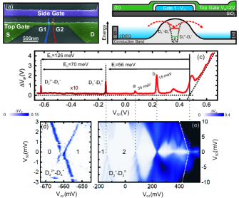
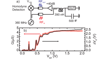
In this study we use a double-gated metal-oxide-semiconductor field-effect transistor to map the energy spectrum of a donor molecule in Si González-Zalba et al. (2012); Angus et al. (2008), as seen in Fig. 1(a). The nanoFETs G1 and G2 control the energy band bending of the environment immediately under it. Setting it below threshold generates a barrier and current only flows through quantum tunneling (Fig. 1(b)). Furthermore, G1(2) tunes the electrochemical levels of the impurities, i.e, the energy required to add an extra electron to the system. Whenever one of these levels resides within the energy window of the bias voltage (centered at VSD), transport through the structure can occur and resonant tunneling current peaks appear. In order to reduce the effect of noise on these devices we used radio-frequency reflectometry Schoelkopf et al. (1998). This technique probes the complex impedance of the device generating a DC output voltage which is proportional to the differential conductance (see Methods).
Up to 12 devices measured at 4 K showed subthreshold resonances associated to individual As atoms — charging energies between 23 and 37 meV, as previously reported for gated donors Calderón et al. (2010); Tan et al. (2009) — with an average of 2 As atoms per transistor. The FET controlled by G1 was the only one presenting resonant lines with enhanced charging and binding energies, signaling a strongly coupled donor pair in the channel of the transistor.
Fig. 1(c) shows the rf-response as a function of the gate voltage (). Below threshold (=470 mV), obtained from a fit to the linear region of the FET, we observe a set of single donor or unintentional quantum dot lines, marked as a and b, located at 34 and 15 meV with respect to the conduction edge (see Methods). Notably, we observe two other transitions, D22+D2+ and D2+D20 at -660 mV and -140 mV respectively, which are the main focus of this paper.
We quantify these energies by measuring the characteristic Coulomb diamonds (Figs. 1(d) and 1(e)). We find a charging energy of =703 meV, read from the axis at the point where the edges of the diamonds meet as to avoid the use of gate-voltage-to-energy conversion parameters that depend on electron occupancy and bias conditions (see Methods). Moreover, the first ionization energy =565 meV is obtained from the point at which the DD transition meets with the edge of the conduction band, indicated by the dotted white lines. The second ionization energy is therefore =1266 meV. These values are markedly larger than expected for an isolated arsenic donor in bulk silicon: =51.71 meV, =2.05 meV (As0As-), and =53.76 meV (As+As0) Calderón et al. (2010).
The naive comparison of the measured values to a rescaled theory of H2 molecules also leads to disappointing results (see Methods). Overcoming these apparent inconsistencies demands a realistic theory of donor pairs in Si. Calculations are performed here within an improved effective mass approach, which includes central cell corrections with an empirical radius leading to the correct A1 energies, the full valley structure of the Si conduction band, and electron-electron correlations through a configuration interaction method. This approach extends previous results Kane (1998); Koiller et al. (2001) to much smaller distances between dopants with higher accuracy. The central cell correction enhances the one and two electron binding energies (Fig. 2(a)) and indirectly enhances the electron-electron repulsion shown in Fig. 2(b), due to the tighter confinement of the A1 states.
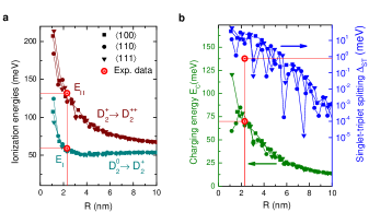
Comparison between theory and experiment leads to the identification of the particular interdonor distance of the molecule. We first compare the ionization energies because of the smooth behavior of these energies with , regardless of the molecular orientation. Both and measurements, indicated in Fig. 2(a), are consistent with an inter-donor distance of nm. This result is also in agreement with the charging energy profile shown in Fig. 2(b) despite its oscillatory behaviour.
We may confirm the molecular nature of these states and learn about the spin configuration and the singlet-triplet splitting from the spin filling sequence of the one and two-electron energy states [Fig. 3(a)]. The exchange coupling in the Heisenberg spin Hamiltonian – the main ingredient in CNOT operations for Kane’s qubits – is determined by the singlet-triplet splitting as . Experimentally, can be accurately identified by monitoring the evolution of the electrochemical potentials () as a function of magnetic field, in this case applied in the plane of the device (Fig. 3(b)). The rate of change with field is given by Lim et al. (2011),
| (1) |
where is the g-factor 2 for donor-bound electrons in Si, 57.8 eV/T the Bohr magneton and the change in total spin of the molecule when an extra electron is added. Filling the molecule with a spin-down (up) electron results in a slope of the chemical potential with magnetic field. In Fig. 3(c) we measure the evolution of as a function of magnetic field up to 10 T.
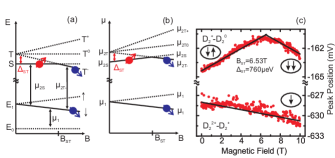
The ground state of the first electron is the lower Zeeman branch, therefore the 0 to 1 electron transition shifts down as a function of field. In Fig. 3(c), the data is compared to a Zeeman shift , calibrated to voltage shift using the lever arm extracted from the slope of the edges of the D2D2+ transition, confirming the loading of a spin-down electron.
Experimentally the two-electron ground state Fig. 3(c) shifts in the opposite direction at low magnetic fields, consistently with the loading of a spin-up electron and a singlet two-electron ground state at low fields. Here, we use extracted from the slopes of the D2D20 transition. At =6.53 T the slope changes to indicating a change in spin configuration, a transition from spin-singlet to spin-triplet two electron ground state. From the magnetic field at which this happens, we extrapolate a zero field singlet-triplet splitting of 0.76 meV.
The small singlet-triplet splitting measured can be explained from the particular molecule orientation leading to destructive interference of the electronic wavefunctions as seen in Fig. 2(b) for the and crystallographic directions. This is a vivid example of the fragility of the singlet-triplet splitting to the particular positioning of donors, as predicted in Ref. Koiller et al. (2001).
Finally we investigate the role of external electric fields since these are known to modify the single-donor spectrum Rahman et al. (2011a). Figure 4(a) shows the effect of a detuning electric field applied along the axis of the molecule for the distance nm. This is accomplished by shifting the on-site energies on the molecular orbital theory by . We disregard here the proximity of interfaces Calderón et al. (2010); Tan et al. (2009). The separation between donors is too small for the electric field to generate a significant detuning. Moreover, the ionization energies are large due to the molecular hybridization, so that the charge states are robust against these external fields. This robustness explains why our theory for bulk Si describes well the energy levels even under the complex environment in our FET devices.
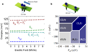
We also study the hypothetical donor-pair separation, nm. In this case, the existence of a classically forbidden region between the two donor sites permits a study of the charge occupation of each site separately. The charge stability diagram, shown in Fig. 4(b), is consistent with the data from Fig. 2 and equivalent to the diagram in a double quantum dot Hanson et al. (2007). The analogy with quantum dots may be explored to implement charge and spin qubits.
The control over the charge degree of freedom at the transition, instrumental for charge qubit proposals Hollenberg et al. (2004), could be implemented with modest electric fields. We estimate the tunnel coupling to be eV from the level anti-crossing around meV.
Interestingly, it is possible to estimate the order of magnitude of the singlet-triplet splitting using the Hubbard model in the limit of small tunneling and large charging energy. This regime (Mott limit) leads to eV, estimating the same-site charging energy meV from the bulk D- energy in As. The actual value calculated within the full configuration interaction method is eV. We expect this approximation to be valid only for nm where a classically forbidden barrier between the sites exists.
Our measurements and theory offer a proof of concept for quantum computation proposals relying on the exchange coupling between electron spins on donors. By analogy with artificial molecules, e.g. GaAs and Si double quantum dots, there is potential for a dopant molecule to be operated as a singlet-triplet spin qubit overcoming current difficulties with Kane’s architecture exchange gates. Such a system would have the dual advantages of enabling spin manipulation via electric, rather than magnetic fields, and the long spin coherence times of dopants in silicon. Moreover, the sample we measure here has an electron-electron spin exchange coupling much larger than the hyperfine coupling with the nuclei, akin to real molecules. This raises the possibility of engineering longer and more complex chains as a playground for quantum chemistry on a chip. The exchange coupling becomes comparable to the As bulk hyperfine coupling MHz at an interdonor distance of nm, which sets the ideal geometry for Kane’s architecture.
I Methods Summary
Experiment. Devices were fabricated on a high-resistive silicon wafer (7000 cm) and low-dose-ion-implanted with arsenic (D=1e11 cm-2, =15 keV). The sacrificial oxide was removed after implant and a 10 nm SiO2 gate oxide was regrown at 850∘C. C-V measurements of similar devices indicate an interface trap charge density of 1.81010 cm-2. The calculated profile gives a dopant density of 5cm-3 at 10 nm from the interface. Two sets of electrically independent e-beam-defined aluminium gates form the structure with nominal channel dimensions l=40 nm and w=120 nm. A positive voltage on the top gate induces an electron accumulation layer which constitutes the source and drain reservoirs of the FET. Measurements were performed at the base temperature of a dilution refrigerator with an electron temperature of 200 mK. Radio-frequency reflectometry was performed at 360 MHz by embeding the sample in a rf-tank circuit formed by a surface mount inductor (390 nH) and the parasitic capacitance to ground (500 fF).
Theory. We adopt the multivalley effective mass theory with the explicit inclusion of a Yukawa-type potential with empirical cut-off radius accounting for the central cell corrections. The effective mass is taken to be isotropic and to reproduce the hydrogenic energy obtained from the anisotropic Kohn-Luttinger model. The envelope function is obtained separately for each of the A1, T2 and E states variationally as 1s Slater-type orbitals. All single-electron integrals are calculated analytically following Ref. Tai (1986). Electron-electron repulsion integrals are calculated within Pople’s STO-2G scheme Hehre et al. (1969). The wavefunction and energy spectrum of the two-electron problem is obtained through spin-adapted configuration interaction (SACI), an exact theory within the chosen basis set which permits the separate analysis of the singlet and triplet subspaces. The two-electron wavefunction radii are obtained minimizing separately the singlet and triplet lowest eigenvalues of the SACI matrices.
II Acknowledgements
The authors thank P.A. Gonzalez for fruitful discussions. MFGZ and AJF acknowledge support from EPSRC grant no. EP/H016872/1 and the Hitachi Cambridge Laboratory. AJF was supported by a Hitachi Research Fellowship. MFGZ was supported by an Obra Social La Caixa fellowship and Gobierno de Navarra Research grant. AS and BK performed this work as part of the Brazilian National Institute for Science and Technology on Quantum Information and also acknowledge partial support from the Brazilian agencies FAPERJ, CNPq, CAPES. MJC acknowledges support from MINECO-Spain through Grant FIS2012-33521.
III Author contributions
MFGZ and AS contributed equally to this work. MFGZ, DH and AJF fabricated the device, performed the measurements and interpreted the data. AS, MJC and BK devised the model. AS and MJC performed the calculations. MFGZ and AS produced the figures. All authors participated in the writing of the paper.
IV Additional information
The authors declare no competing financial interests.
V Methods
Device fabrication. The device fabrication starts by growth of a 10 nm sacrificial oxide on a high-resistivity (7000 cm) (100) silicon wafer. Ohmic contacts were defined by optical lithography and ion implantation of phosphorus (15 keV, cm-2) and dopants included by low-dose (15 keV, cm-2) ion-implantation of arsenic. The sacrificial silicon oxide was removed after the implant and a 10 nm SiO2 gate oxide was regrown at 850∘C, which also anneals out the implantation damage. A forming gas anneal at 450∘C for 30 min was performed followed by a rapid thermal anneal for 15 s at 1050∘C to reduce the interface trap and fixed oxide charge density. The As profile was calculated by an implantation Monte-Carlo simulator Ziegler and has a maximum at 10 nm from the interface and a peak density of 51016cm-3 resulting in a statistical mean inter-dopant distance of 27 nm. However, the expected segregation of As towards the interface during the subsequent thermal processing leads to an increase in the donor density at the interface and favours clustering Grove et al. (1964). By comparison, the residual phosphorus doping is estimated to be smaller than 1012 cm-2.
Subsequent to the silicon processing, surface gates were fabricated by electron beam lithography and thermal evaporation of aluminium. Fig.1(a,b) shows a scanning electron microscopy image of an identical device and its schematic cross-section. As a first step, two gates 40 nm wide and 100 nm apart were defined by evaporation of a 25 nm thick layer of aluminium. They are used to form the tunable source and drain tunnel barriers. After thermal oxidation at 150∘C for 5 min creating a 5 nm AlOx layer, a second electrically-independent 60 nm thick top gate was deposited over the barriers. This top-gate defines the 120 nm wide channel of the SET and leads that overlap with the doped ohmic contacts. From the lithographical dimensions of the two sets of gates it is possible to estimate an average number of 2 As atoms per tunnel barrier. Prior to measurement the samples undergo a nitrogen ambient post-fabrication anneal at 350∘C for 15 min. The interface trap density, measured on simultaneously processed field effect transistors, without e-beam radiation, by means of low frequency split C-V method Koomen (1973), is 1.81010cm-2.
Measurement techniques. Electrical transport measurements were performed at the base temperature of a dilution refrigerator (electron temperature of 200 mK) using radio-frequency reflectometry Schoelkopf et al. (1998). This technique probes the reflection coefficient of a resonant circuit that includes the device as a circuit element (Fig. 5(a)). As the impedance, in this case the differential conductance, of the device changes so does the reflection coefficient of the resonant circuit (Fig. 5(b)). This technique allows an increase of bandwidth over a standard DC or lock-in measurement. The sample was embedded in a rf-tank circuit formed by a surface mount 390 nH inductor and a parasitic capacitance (500 fF) to ground. An rf-carrier signal was applied to the source of the device at the resonant frequency of 360 MHz and the cryo-amplified reflected signal is homodyne detected Angus et al. (2008). A bias tee on the sample board permitted the simultaneous measurement of the two terminal DC conductance. The measurements presented here have been obtained after a bias cool down, ===1 V. When performing transport spectroscopy of the SB device the TG and DB was set well-above threshold (==2 V). The devices survived several thermal cycles preserving the subthreshold transitions independently of the bias during the cool-down, confirming its atomic origin.
Experimental considerations. Due to the electrostatic configuration of our device in Fig. 1(b), transport spectroscopy senses only impurities close to the interface immediately below the barrier electrode. The electrostatic properties of single dopants are modified by the presence of an electric field Rahman et al. (2011a): For gated donors a reduction in due to screening effects has been experimentally observed Lansbergen et al. (2008), while there is experimental evidence of an enhanced in systems under quantum confinement Diarra et al. (2007), which is very unlikely to occur for the planar geometry of our device. The possible effect of the dielectric mismatch cannot explain quantitatively in any case the observed energy enhancement Calderón et al. (2010) ruling out any of the aforementioned mechanism as the origin of the simultaneous increase of the binding and charging energies.
In order to obtain highly accurate values of the binding and charging energies we consider the point in at which the edges of the Coulomb diamonds meet. Conventionally a constant voltage-to-energy calibration parameter , where is the energy at the dopant site, is used to obtain energy values from gate voltage changes Pierre et al. (2009). However, under the considerations of the constant interaction model, this is expected to be different for different electronic occupations of the molecule as experimentally observed here. Moreover, could vary with bias conditions Sellier et al. (2006) reducing the accuracy of this method.
The states a, b in Fig. 1(c) have been described elsewhere as single dopant states or unintentional quantum dots generated due to potential irregularities at the interface González-Zalba et al. (2012).
Theory. The theory of H2 molecules in vacuum could be rescaled by the effective semiconductor energy and distance atomic scales, but the results are misleading. In order to get values comparable to the measured ones we have to reach the hypothetical limit of where the two atoms merge into a He-like atom with meV, meV, and meV. The equivalent of a He atom in Si would be a group VI donor – S, Se, or Te – but the accidental presence of these is highly unlikely and the binding energies for these dopants are much larger Grimmeiss et al. (1982) than the ones measured here (e.g. for S, these values are respectively meV, meV and meV). Moreover, the singlet-triplet splitting measured here is smaller than the rescaled splitting between ortho and parahelium by two orders of magnitude.
We take the impurity potential to reflect the complications associated with the departure from the hydrogenic model. The deviation of from the point charge screened coulomb potential has its roots on the finite screening length, the structure of the electronic cloud of valence electrons and the covalent bonds. All these effects modify the effective impurity potential at the scale of the atomic radius, which is much smaller than the typical size of the wavefunction of shallow impurities in the hydrogenic model . Only the first effect can be taken into account without getting into the details of the chemical nature of the donor. The most common approach is to consider an usual point charge potential modified by a semi-empirical central cell correction. This way, we write the full impurity potential as the superposition of the uniformly screened point charge hydrogenic potential
| (2) |
and a central cell correction term . Here we take an approach inspired by the Yukawa potential
| (3) |
This form gives the correct physical limits for at and , and the characteristic radius of the central cell region is the only empirical parameter in our theory. We take pm to fit the experimental valley splitting. A similar approach was adopted by Wellard and Hollenberg Wellard and Hollenberg (2005), with their empirical parameter rescaling the dielectric function to fit the experimental energy.
The multivalley solution to this problem is well known. The lowest energy manifold consists of 1s-like envelopes and combinations of band minima Bloch functions which may be written as . The particular combinations that transform according to the tetrahedral crystal field ( symmetry) are , , , , and .
These states are split if we take into account the the intervalley coupling due to the crystal field potential, leading to a non-degenerate ground state (A1), a three-fold degenerate first excited state (T) and a doubly degenerate second excitation(E). Nevertheless, the mere inclusion of the intervalley integrals of the Coulomb potential severely underestimates the separation between the excitation energies Wellard and Hollenberg (2005).
The most prominent source of splittings comes from the central cell correction discussed above, which acts differently on the six states. While A1 is even under reflections on the cartesian planes around the donor site, T and E are odd, so that in the region where the central cell correction is most active (), has a peak while all the and have a node, and therefore nearly vanish. Indeed, the experimental binding energies of the and states are reasonably described by the hydrogenic model, while the binding energy is considerably larger.
The Kohn-Luttinger model treats this splitting empirically, while no correction to the wavefunction localization is made. Kohn Kohn (1957) pointed out that the asymptotic behavior of the wavefunction is expected to be significantly altered by the central cell correction, leading to states more localized than the excited states. Following this argument, we ascribe different wavefunction variational decay radii nm for the central cell corrected state (obtained variationally from the hamiltonian with the full impurity potential ) and nm for all the T and E states (which results directly from solving the hydrogenic problem and disregarding ). The variational energy obtained is exactly the experimental energy by construction (by fitting ).
The two donors, referred to as and , located at positions and are separated by a vector . The crystal defines cartesian directions, so that the energy and wavefunction of an electron at a position depends on the full vector and not only on the distances to the point charges and — differently from the analogue H problem. This is not clear from the effective mass hamiltonian of a double donor, which reads
| (4) |
The matrix elements of this hamiltonian are calculated in the molecular orbital approximation, i.e., in the basis set defined by the six valley combinations centered at and , so that the hamiltonian is a 1212 matrix composed of four blocks
| (5) |
Blocks and are diagonal and represent the on-site energies, while the tunnel coupling is determined by the blocks and . The hamiltonian above is symmetric under the exchange of . Later we will study the system in which this symmetry is broken introducing a detuning potential.
The diagonal blocks read , showing that the onsite energy consists of the single donor binding energies (for A1 states) and (for E and T states), corrected by a long range classical term which reads for A1 states and for E and T states. It is interesting to notice that, due to the periodicity of the Bloch functions, the same argument regarding the different effect of the central cell on A1 and T/E states apply here. In other words, the state presents a peak at the B site and is influenced by the central cell of the B impurity , while the and states present a node and are immune to the central cell correction.
The off diagonal terms in and are only approximatly vanishing, since with the presence of the second donor the problem looses its spherical symmetry. But direct calculation reveal this to be a good approximation.
The off-diagonal blocks are related by the hermiticity condition . Each term is a summation over integrals of the type
| (6) |
These matrix elements can be straightforwardly calculated using the plane wave expansion of the Bloch functions (see Ref. Saraiva et al., 2011), and no further approximation is necessary. Nevertheless, it is useful to express these integrals in a simpler form adopting some very robust and well tested approximations: (i) taking the matrix elements for to be vanishing, since these consist of rapidly oscillatory integrands; (ii) taking , as suggested in Ref. Saraiva et al., 2011. With these, we write
| (7) |
where is the single valley tunnel coupling
| (8) |
The effect of the hopping blocks is analogous to the H2 molecule – at distances much larger than and , this block is null and the states centered around sites A and B are degenerate, while for distances comparable to the wavefunction radius there is the formation of symmetric and antisymmetric superpositions of the localized orbital with splitted energies. Unlike the H2 analogue, it is possible for the antisymmetric state (referred to as antibonding in the context of H2 in vacuum) to be the ground state here, since the hoppings are not necessarily real negative numbers due to the oscillatory phase .
The same oscillatory phase may also lift the degeneracies of the T and E states. For instance, if the pair alignment is along the direction, the states and are still equivalent, while the state will have a symetric-antisymmetric splitting that oscillates as a function of .
It is known from the H2 problem that the molecular orbital approximation gives accurate results only if the variational wavefunction radius is taken to minimize the expectation value of the complete hamiltonian containing the two protons. We do the same here, minimizing numerically the lowest eigenvalue of the double donor hamiltonian with relation to all the six wavefunction radii .
Given the solution of the problem of one electron with two donors discussed above, we may use these 12 molecular orbitals to write down spin-orbitals from Slater determinants. Combining suitably the Slater determinants, we may identify 78 spin singlets and 66 triplets (for a total of two-electron spin-orbitals). These include all possible excitations of the two electrons. Calculating the matrix elements of the full hamiltonian, including the electron-electron repulsion, we may obtain the full configuration interaction ground state. Since we explicitly disconnect the singlet and triplet blocks, this method is often referred to as Spin Adapted Configuration Interaction, or SACI.
The explicit calculation of the two-electron exchange and hybrid integrals is an outstanding problem in computational quantum chemistry, and is often solved approximately. One of the most successful approaches is to fit a number of gaussian orbitals to the Slater-type orbital obtained in the single electron problem. This basis set, called STO-G, converges quickly Hehre et al. (1969). We tested and without significant improvement. All data presented is for , though.
Our method is therefore well tested and robust in all regimes except at distances comparable to the central cell region. At this region, the polarization cloud around the donor nuclei is non-trivial and the effective potential acting on conduction electrons is most likely non-additive. Therefore, this theory is not capable of describing vicinal donors (substituting first nearest neighbor Si sites). We set a minimum distance of nm as a conservative boundary for our theory.
References
- Kane (1998) B. E. Kane, Nature 393, 133 (1998), ISSN 0028-0836.
- Hollenberg et al. (2004) L. C. L. Hollenberg, A. S. Dzurak, C. Wellard, A. R. Hamilton, D. J. Reilly, G. J. Milburn, and R. G. Clark, Physical Review B 69, 4 (2004), ISSN 1098-0121.
- Morello et al. (2010) A. Morello, J. J. Pla, F. A. Zwanenburg, K. W. Chan, H. H. M. Mottonen, C. D. Nugroho, C. Yang, J. A. van Donkelaar, A. Alves, D. N. Jamieson, et al., Nature 467, 687 (2010).
- Pla et al. (2012) J. J. Pla, K. Y. Tan, J. Dehollain, W. H. Lim, J. L. Morton, D. N. Jamieson, A. S. Dzurak, and A. Morello, Nature 489, 541 (2012).
- Pla et al. (2013) J. J. Pla, K. Y. Tan, J. Dehollain, W. H. Lim, J. L. Morton, F. A. Zwanenburg, D. N. Jamieson, A. S. Dzurak, and A. Morello, Nature 496, 334 (2013).
- Koenraad and Flatte (2013) P. M. Koenraad and M. E. Flatte, Nature Materials 10, 91 (2013), ISSN 1476-1122, URL http://dx.doi.org/10.1038/nmat2940.
- Zwanenburg et al. (2013) F. A. Zwanenburg, A. S. Dzurak, A. Morello, M. Y. Simmons, L. C. L. Hollenberg, G. Klimeck, S. Rogge, S. N. Coppersmith, and M. A. Eriksson, Rev. Mod. Phys. 85, 961 (2013).
- Lansbergen et al. (2008) G. P. Lansbergen, R. Rahman, C. J. Wellard, I. Woo, J. Caro, N. Collaert, S. Biesemans, G. Klimeck, L. C. L. Hollenberg, and S. Rogge, Nature Physics 4, 656 (2008).
- Fuechsle et al. (2012) M. Fuechsle, J. A. Miwa, S. Mahapatra, H. Ryu, S. Lee, O. Warschkow, L. C. L. Hollenberg, G. Klimeck, and M. Y. Simmons, Nature Nanotechnology 7, 242 (2012).
- Asenov et al. (2003) A. Asenov, A. R. Brown, J. H. Davies, S. Kaya, and G. Slavcheva, IEEE Transactions on Electronic Devices 50, 1837 (2003), ISSN 0018-9383.
- Shinada et al. (2005) T. Shinada, S. Okamoto, T. Kobayashi, and I. Ohdomari, Nature 437, 1128 (2005), ISSN 0028-0836, URL <GotoISI>://000232660500038.
- Pierre et al. (2009) M. Pierre, R. Wacquez, X. Jehl, M. Sanquer, M. Vinet, and O. Cueto, Nature Nanotechnology 5, 133 (2009).
- Sellier et al. (2006) H. Sellier, G. P. Lansbergen, J. Caro, S. Rogge, N. Collaert, I. Ferain, M. Jurczak, and S. Biesemans, Phys. Rev. Lett. 97, 206805 (2006).
- Ono et al. (2007) Y. Ono, K. Nishiguchi, A. Fujiwara, H. Yamaguchi, H. Inokawa, and Y. Takahashi, App. Phys. Lett. 90, 102106 (2007), ISSN 0003-6951, URL <GotoISI>://WOS:000244791700047.
- Tan et al. (2009) K. Y. Tan, K. W. Chan, M. Möttönen, A. Morello, C. Yang, J. v. Donkelaar, A. Alves, J.-M. Pirkkalainen, D. N. Jamieson, R. G. Clark, et al., Nano Letters 10, 11 (2009), ISSN 1530-6984, URL http://dx.doi.org/10.1021/nl901635j.
- Rahman et al. (2011a) R. Rahman, G. P. Lansbergen, J. Verduijn, G. C. Tettamanzi, S. H. Park, N. Collaert, S. Biesemans, G. Klimeck, L. C. L. Hollenberg, and S. Rogge, 84, 115428 (2011a), URL http://link.aps.org/doi/10.1103/PhysRevB.84.115428.
- Calderón et al. (2010) M. J. Calderón, J. Verduijn, G. P. Lansbergen, G. C. Tettamanzi, S. Rogge, and B. Koiller, Phys. Rev. B 82, 075317 (2010).
- Roche et al. (2013) B. Roche, R. P. Riwar, B. Voisin, E. Dupont-Ferrier, R. Wacquez, M. Vinet, M. Sanquer, J. Splettstoesser, and X. Jehl, Nature Communications 4, 5 (2013), ISSN 2041-1723.
- Lansbergen et al. (2012) G. P. Lansbergen, Y. Ono, and A. Fujiwara, 12, 763 (2012), ISSN 1530-6984, URL http://dx.doi.org/10.1021/nl203709d.
- Tabe et al. (2010) M. Tabe, D. Moraru, M. Ligowski, M. Anwar, R. Jablonski, Y. Ono, and T. Mizuno, Phys. Rev. Lett. 105, 016803 (2010), ISSN 0031-9007, URL <GotoISI>://WOS:000279485500002.
- Roche et al. (2012) B. Roche, E. Dupont-Ferrier, B. Voisin, M. Cobian, X. Jehl, R. Wacquez, M. Vinet, Y.-M. Niquet, and M. Sanquer, Phys. Rev. Lett. 108, 206812 (2012), URL http://link.aps.org/doi/10.1103/PhysRevLett.108.206812.
- Prati et al. (2012) E. Prati, M. Hori, F. Guagliardo, G. Ferrari, and T. Shinada, Nature Nanotechnology 7, 443 (2012), ISSN 1748-3387.
- Dupont-Ferrier et al. (2013) E. Dupont-Ferrier, B. Roche, B. Voisin, X. Jehl, R. Wacquez, M. Vinet, M. Sanquer, and S. De Franceschi, Physical Review Letters 110, 5 (2013).
- Miller and Abrahams (1960) A. Miller and E. Abrahams, Physical Review 120, 745 (1960), URL <GotoISI>://INSPEC:1960A18013.
- Koiller et al. (2001) B. Koiller, X. Hu, and S. Das Sarma, Physical Review Letters 88, 027903 (2001).
- Zhang et al. (2013) G. G. Zhang, A. Canning, N. Gronbech-Jensen, S. Derenzo, and L. W. Wang, Physical Review Letters 110, 5 (2013), ISSN 0031-9007.
- Rahman et al. (2011b) R. Rahman, S. H. Park, G. Klimeck, and L. C. L. Hollenberg, Nanotechnology 22, 9 (2011b).
- González-Zalba et al. (2012) M. F. González-Zalba, D. Heiss, and A. J. Ferguson, New Journal of Physics 14, 023050 (2012).
- Angus et al. (2008) S. J. Angus, A. J. Ferguson, A. S. Dzurak, and R. G. Clark, Applied Physics Letters 92, 112103 (2008), URL http://scitation.aip.org/content/aip/journal/apl/92/11/10.1063/1.2831664.
- Schoelkopf et al. (1998) R. J. Schoelkopf, P. Wahlgren, A. A. Kozhevnikov, P. Delsing, and D. E. Prober, Science 280, 1238 (1998), ISSN 0036-8075.
- Lim et al. (2011) W. H. Lim, C. H. Yang, F. A. Zwanenburg, and A. Dzurak, Nanotechnology 22, 335704 (2011), ISSN 0957-4484, URL http://stacks.iop.org/0957-4484/22/i=33/a=335704.
- Hanson et al. (2007) R. Hanson, L. P. Kouwenhoven, J. R. Petta, S. Tarucha, and L. M. K. Vandersypen, Rev. Mod. Phys. 79, 1217 (2007), URL http://link.aps.org/doi/10.1103/RevModPhys.79.1217.
- Tai (1986) H. Tai, Physical Review A 33, 3657 (1986), ISSN 1050-2947, iSI Document Delivery No.: C5832 Times Cited: 9 Cited Reference Count: 24 Tai, h 9 American physical soc College pk, URL <GotoISI>://WOS:A1986C583200002.
- Hehre et al. (1969) W. J. Hehre, R. F. Stewart, and J. A. Pople, Journal of Chemical Physics 51, 2657 (1969), ISSN 0021-9606, iSI Document Delivery No.: E3382 Times Cited: 4497 Cited Reference Count: 30 Hehre, wj stewart, rf pople, ja 4496 Amer inst physics Woodbury, URL <GotoISI>://WOS:A1969E338200047.
- (35) J. Ziegler, SRIM-the stopping and range of ions in matter.
- Grove et al. (1964) A. S. Grove, O. Leistiko, and C. T. Sah, Journal of Applied Physics 35, 2695 (1964), URL http://scitation.aip.org/content/aip/journal/jap/35/9/10.1063/1.1713825.
- Koomen (1973) J. Koomen, Solid-State Electronics 16, 801 (1973), ISSN 0038-1101, URL http://www.sciencedirect.com/science/article/pii/0038110173901779.
- Diarra et al. (2007) M. Diarra, Y.-M. Niquet, C. Delerue, and G. Allan, Phys. Rev. B 75, 045301 (2007).
- Grimmeiss et al. (1982) H. G. Grimmeiss, E. Janzén, and K. Larsson, Phys. Rev. B 25, 2627 (1982).
- Wellard and Hollenberg (2005) C. J. Wellard and L. C. L. Hollenberg, Phys. Rev. B 72, 085202 (2005).
- Kohn (1957) W. Kohn, Solid State Physics Series, vol. 5 (Academic Press, 1957), edited by F. Seitz and D. Turnbull.
- Saraiva et al. (2011) A. L. Saraiva, M. J. Calderón, R. B. Capaz, X. Hu, S. Das Sarma, and B. Koiller, Phys. Rev. B 84, 155320 (2011).