Giant Photogalvanic Effect in Metamaterials
Containing Non-Centrosymmetric Plasmonic Nanoparticles
Abstract
Photoelectric properties of metamaterials containing non-centrosymmetric, similarly oriented metallic nanoparticles embedded in a homogeneous semiconductor matrix are theoretically studied. Due to the asymmetric shape of the nanoparticle boundary, photoelectron emission acquires a preferred direction, resulting in a photocurrent flow in that direction when nanoparticles are uniformly illuminated by a homogeneous plane wave. This effect is a direct analogy of the photogalvanic (or bulk photovoltaic) effect known to exist in media with non-centrosymmetric crystal structure, such as doped lithium niobate or bismuth ferrite, but is several orders of magnitude stronger. Termed the giant plasmonic photogalvanic effect, the reported phenomenon is valuable for characterizing photoemission and photoconductive properties of plasmonic nanostructures, and can find many uses for photodetection and photovoltaic applications.
pacs:
79.60.Jv, 73.20.Mf, 78.67.Bf, 85.30.Kk, 78.67.Pt.I Introduction
The recent decade in modern physics has featured the concept of optical metamaterials. The central idea of this concept is to bestow the role of known, ordinary constituents of matter (atoms, ions, or molecules) upon artificial “meta-atoms”—nanosized objects purposely designed to have the desired optical properties mmBook . The assembly of such meta-atoms—an artificial composite metamaterial—exhibits the desired properties macroscopically, provided that the meta-atoms are much smaller than the wavelength of light interacting with them.
Great as the variety of naturally occurring atoms and molecules (and, in turn, of natural materials) may be, the inherent total freedom in choosing the shape and composition of artificial meta-atoms is believed to be even greater—nearly arbitrary. Thus, a prominent success of optical metamaterials is the design of materials with optical properties that either do not exist or are much weaker in naturally occurring media. Notable examples include metamaterials with a negative refractive index, near-zero, or very large permittivity; metamaterials with magnetic permeability at optical frequencies; extremely anisotropic hyperbolic metamaterials that behave like metals in some directions and like dielectrics in others; chiral metamaterials with giant magnetooptical properties, and many others mm1 ; mm2 ; mm3 .
Most meta-atom designs proposed to date are based on metallic nanoparticles, nanoantennas, or resonators of various shapes mmAnt . In such metallic structures, the size prerequisite for meta-atom design is fulfilled by subwavelength confinement of electromagnetic field due to localized surface plasmon resonance excitation. At the same time, localized plasmons are known to cause strong local field enhancement, which can enhance the functionality of metamaterials in the context of biological and chemical sensing, as well as give rise to new concepts of optical metamaterials based on strongly enhanced nonlinear, photorefractive, and photoconductive effects. In particular, plasmonics-enhanced photoconductivity–the emission of photoelectrons from nanoparticles due to action of strong local fields in the localized plasmonic resonances–was recently shown to be promising for photodetection and photovoltaic applications NordlanderNatC13 ; NordlanderNL13 ; ourPlas .
Transcending the purely electromagnetic approach traditionally adopted in the study of plasmonic nanostructures and accounting for processes when light can cause electrons to leave the nanoparticles has far-reaching implications, putting forth a new concept of photoconductive metamaterials. The enhanced photoelectric effect from plasmonic nanoantennas with generation of “hot” electrons uGovorov ; uReview1 can be used to improve the characteristics of light-harvesting devices (e.g., photoconductive plasmonic metamaterials, photodetectors, solar and photochemical cells) uCarius13 ; uCatchpole12 ; uHalasSci11 ; uMisawa10 ; uMoskovits13 ; uTatsuma11 ; plas5-UskovUFN12 ; plas8-Novitsky12 ; uGovorov ; uReview1 ; uAtwater14 , as well as more generally in optoelectronics, photochemistry, and photo electrochemistry ch1-Small ; ch2-Nanoscale ; ch3-SREP .
In this paper, we predict and numerically demonstrate an effect related to new functionality of photoconductive metamaterials: the giant plasmonic photogalvanic effect. Named after photogalvanic (or bulk photovoltaic) effect in bulk non-centrosymmetric media bookSturmanFridkin , plasmonic photogalvanic effect is shown to exist in a metamaterial containing similarly oriented non-centrosymmetric metallic nanoparticles embedded in a homogeneous semiconductor matrix. The low degree of symmetry of the nanoparticle shape causes the net flux of the “hot” electrons emitted from the nanoparticles via the resonant plasmonic excitation to be directional. This directionality leads to a photo-electromotive force as a result of homogeneous external light illumination (the photogalvanic effect).
We report that the resulting photocurrent density generated in a layer of nanoparticles emerges and grows as the particle shape changes from cylindrical to conical, i.e., with the increase of the particle asymmetry. We calculate the components of the effective third-rank tensor relating the current density to the incident electric field, and show that this effective tensor for the nanoparticle array exceeds that for the naturally occurring ferroelectrics that exhibit bulk photovoltaic effect. Hence, the reported plasmonic effect can be regarded as a “giant” version of the conventional (non-plasmonic) photogalvanic effect occurring in natural materials.
The paper is organized as follows. In Section II we review the theoretical background for “hot” electron photoemission at metal-semiconductor interfaces containing Schottky barriers. In Section III we numerically investigate arrays of nanoparticles whose shape varies from cylindrical to conical. We discuss the observed increase of photocurrent directionality and induced electromotive force as a result of increased spatial asymmetry of the nanoparticles. In Section IV we draw parallels between the predicted plasmonic photogalvanic effect and the known photogalvanic effect in certain naturally occurring media. Finally, in Section V we summarize and outline possible applications for the proposed effect.
II Theoretical background
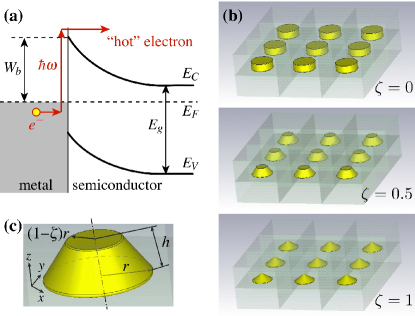
We consider a metallic nanoparticle embedded in a uniform semiconductor matrix (Fig. 1) in presence of a normally incident light wave of frequency , such that
| (1) |
It is assumed that the photon energy is insufficient to excite electron-hole pairs in the semiconductor matrix with gap energy , but exceeds the work function for the metal/semiconductor interface (see Fig. 1a), so that the photon energy transferred to an electron in metal can cause it to leave the nanoparticle.
Two mechanisms of energy transfer from the photon to the electron can be identified plas22-Tamm31 ; plas23-BrodskyBook ; plas24-BrodskyJETP . One is absorption of a photon by an electron in the bulk of the nanoparticle with subsequent transport of the “hot” electron to the surface and its emission by overcoming the Schottky barrier (the volume photoelectric effect plas25-Berini10 ). The other is absorption of a photon by an electron as it collides with the nanoparticle boundary, causing emission of that particular electron from the metal (the surface photoelectric effect). In both of these mechanisms, the spatial and momentum distribution of the emitted electrons is strongly influenced by (i) the spatial configuration of the nanoparticle surface and (ii) resonant field enhancement near that surface due to the plasmonic resonance.
While the question on which of the two mechanisms is stronger in nanostructures is yet to be answered, it was shown that electron collisions after photon absorption leading to rapid “hot” electron cool-down make surface-driven effects prevail over bulk effects in many cases plas22-Tamm31 ; ourTammBulk . So, following the previously developed Tamm theory of photoemission from plasmonic nanoparticles plas5-UskovUFN12 ; plas8-Novitsky12 ; ourPlas , we can express the photocurrent from a nanoparticle as
| (2) |
The integration is performed over the surface of the nanoparticle. The expression in Eq. (2) only takes into account the increased number of photoelectrons without account for the direction of their momentum as they leave the nanoparticle. As a quantity integrated for all electrons in all directions, it is applicable in the photoconductivity scenario when the emitted electrons are subsequently directed using an externally applied or a built-in potential, and their momentum direction upon leaving the nanoparticle can thus be totally disregarded.
In the absence of such potential, the initial velocity of the emitted photoelectrons starts to play a role in the definition of the photocurrent from a nanoparticle, which then has to assume a modified form,
| (3) |
where is the unit normal vector at the nanoparticle surface at point . In both Eqs. (2) and (3), the coefficient equals
| (4) |
where is the refractive index of the matrix and is the external quantum efficiency of the electron photoemission through the potential barrier at the metal/matrix interface ourPlas ; ourSpecIssue ; it strongly depends on the photon energy and varies from zero at (see Fig. 1a) to non-zero values for higher photon energies ourTammBulk . The admittance (inverse impedance) of the matrix medium relates the intensity of a plane wave with the electric field strength as .
When a plasmonic resonance is excited in the nanoparticle, the amplitude of the resonant fields inside it and near its surface usually greatly exceeds the amplitude of the incident field. Therefore, we can see from Eqs. (2)–(3) that in nanoparticles with centrosymmetric shapes (such as nanospheres, nanocubes, or nanodisks) the spatial symmetry of the resonant modes will lead to the cancellation of the directed photocurrent, so that even though . In other words, even though the incident wave can cause additional photoelectrons to be emitted over the Schottky barrier, the collective motion of these electrons will not induce an electromotive force.
The situation changes drastically when the shape of the nanoparticle and/or the field distribution of the resonant plasmonic mode lacks the center of symmetry. Eq. (3) then shows that the resulting photocurrent acquires directionality, so that photoemission from such a non-centrosymmetric nanoparticle results in net photocurrent () and induces electromotive force. The ratio , which can vary from 0 to 1, can be regarded as a measure of directionality for photoemission with respect to one nanoparticle.
In a metamaterial comprising an oriented arrangement of such non-centrosymmetric nanoparticles that is not too dense, the satisfactory approximation is that the neighboring particles do not modify the plasmonic resonance of each other in a significant way. In this case, the individual photocurrents from each particle sum up, with the resulting current density from a square nanoparticle lattice with period written as . Since the nanoparticles are axially symmetric with respect to the -axis (see Fig. 1c), and the lattice has 4-fold rotational symmetry, we expect that for a normally incident wave and , so we can write
| (5) |
where is the field incident on the lattice, and
| (6) |
relates the incident field with the local field and has the meaning of a field enhancement factor due to the localized plasmon resonance in the nanoparticles ourPlas ; ourSpecIssue . If the incident field is, e.g., -polarized, Eq. (5) can be rewritten as
| (7) |
which has the form equivalent to the photocurrent induced in some media with non-centrosymmetric crystal structure due to the photogalvanic (or bulk photovoltaic) effect Fridkin2001 ; bulkYoungPRL ; galvPhysE ,
| (8) |
where are again the components of the incident field, and coefficients , related to the components of the third-rank piezoelectric tensor Fridkin2001 , are non-zero only for noncentrosymmetric media. Examples include piezoelectrics or ferroelectrics such as , quartz with -centers, or -GaAs Fridkin2001 . We see that the photocurrent in Eq. (8) is nonlinear (quadratic) with respect to the field strength .
We can also rewrite Eq. (8) in a modified form bulkFridkinBatirov ,
| (9) |
where is the component of the incident light polarization vector, and is its intensity. In SI units, the components of the tensor have the dimension of inverse volts; normalized by the absorption coefficients, are related to the Glass coefficients for the high-voltage bulk photovoltaic effect in nonlinear crystals bulkFridkinBatirov ; GlassCoefs . One can similarly rewrite Eq. (7), introducing the plasmonic equivalent of Eq. (9) as
| (10) |
We see that Eq. (7) is formally equivalent to Eq. (8), standard for describing the photogalvanic effect in bulk media. However, one important difference has to be noted. In bulk media, directed photoelectrons are generated throughout the volume of the material. They have a finite lifetime since their initial velocity decays as they move. Hence the coefficients in Eq. (8) are proportional to that lifetime bookSturmanFridkin . In contrast, the geometry in Fig. 1b considered here deals with the injection of directed photoelectrons from a nanoparticle array into the surrounding medium. Hence there is no lifetime in Eqs. (5) and (7), which is emphasized by using a tilde over the coefficients in that formula. The behavior of photoelectrons after they have been emitted is a subject for further discussion. It is expected that when many nanoparticle layers are stacked together, the photoelectrons can be recaptured and re-emitted, and in the case of bulk metamaterial the effective lifetime for the directionally emitted electrons could be reintroduced.
III Directional photoemission
from conical nanoparticles
To confirm the predicted photogalvanic effect in a plasmonic metamaterial, we consider an array of gold nanoparticles whose shape is gradually varied from cylindrical to conical (Fig. 1b–c). The choice of conical nanoparticles is well-motivated from a fabricational standpoint, since nanodisks fabricated using lithographic means often acquire asymmetry and resemble cone-like shapes pracAtwaterAM10 ; revAtwater ; other asymmetric shapes such as hemispheres and nanopyramids are also readily fabricable using various techniques as1-Nakayama ; as2-Opal ; as3-Odom .
Let the nanocones under study have height ; the larger (bottom) facet has radius , and the radius of the smaller (top) facet is given by so that can be understood as the “asymmetry” or “conicity” parameter. The case corresponds to the centrosymmetric, disk-shaped particles, whereas the opposite case corresponds to maximally asymmetric nanocones. For the computational example, we use nm and nm.
Permittivity of gold was described by the Drude model with plasma frequency and collision frequency drude . The particles are embedded in a homogeneous GaAs matrix (, eV, eV), which results in the operating range between 870 and 1550 nm according to Eq. (1). For Au/GaAs interface, the values of range from zero at to about 0.0025 for ourTammBulk . The particles are arranged in a 2D square lattice with period nm. According to the earlier results plas8-Novitsky12 ; ourPlas , such a dense lattice prevents the appearance of higher-order diffraction and ensures that the lattice effects are outside of the operating range, so the resonant mode of a particle in a lattice largely coincides with that of an isolated particle ourPlas . Another benefit of making the lattice dense is the increase of the nanoparticles concentration, resulting in the increase of the total induced photocurrent as per Eq. (5).
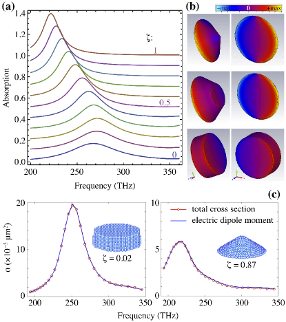
Simulations were carried out in the frequency domain using CST Microwave Studio. The results show that all the structures in question feature a rather broad absorption resonance corresponding to the excitation of a localized surface plasmon (Fig. 2a). As expected, small makes the lattice-related resonances occur outside of the operating frequency range, so the resonance is dominated by the response of a single plasmonic nanoparticle, broadened due to the presence of many of them ourPlas . Note that to reduce the influence of the discretization (“staircasing”) artifacts at sharp edges (which would anyway be unphysical from the fabricational point of view), all edges of the nanoparticles were smoothed with the curvature radius of nm. Together with the adaptive mesh refinement, this proved successful in eliminating numerical artifacts from meshing-related “hot spots”.
We further see that the resonance strongly depends on the nanoparticle shape plas8-Novitsky12 . As the shape changes from a cylinder to a cone, the resonance undergoes a very slight blue shift up to ; further increase of leads to a strong red shift accompanied by a rather significant narrowing of the resonance. Plotting the normal component of the resonant mode field on the nanoparticle surface (Fig. 2b), we notice that although the field at the smaller base (or tip) of the cone becomes progressively weaker as increases, the mode maintains the characteristic outside field pattern of a fundamental dipole resonance for all nanoparticles. To reconfirm this, we have calculated the extinction cross-section of conical nanoparticles using the discrete dipole approximation (DDA) method DDA1 ; DDA2 . Figure 2c shows that extinction properties of the nanoparticles are fully reproduced if only the electric dipole moment is kept in the cases of both low and high asymmetry.
The DDA results reproduce the red shift of the resonance as increases, which is qualitatively similar to what happens in a metal spheroid as it becomes more oblate DDAspheroid . Moreover, the results in Fig. 2c show the decrease of the effective dipole moment of a nanocone compared to a nanodisk. This decrease diminishes the coupling between the individual particles in the lattice, weakening the absorption peak broadening for larger , which is though to be the primary mechanism of the resonance narrowing for the nanocones.
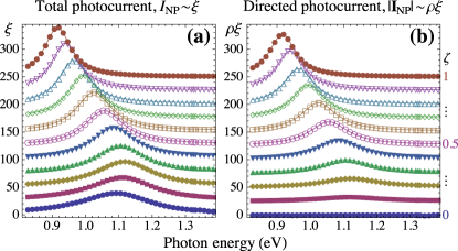
From the distribution of the local field at the nanoparticle surface, which was determined numerically at every frequency, we then calculate the photoemission current from each nanoparticle using Eqs. (2) and (3). The results are shown in Figs. 3a–b, respectively. It can be seen that the cylindrical nanoparticles have no preferred direction of the emitted photoelectrons. However, the more the nanoparticle shape evolves towards conical with -axis symmetry, the greater directionality along the -axis the photoelectrons acquire.
The sign of indicates that electrons tend to be emitted in the direction of the base of the cone. This can be explained by the field distributions in Fig. 2b. In a nanodisk, the two facets have equal field distribution and therefore photocurrent resulting from emission from the two facets balances each other; the same happens with the side walls, resulting in overall . In a cone, the field distribution (and hence, photoemission) at its base is similar to the facet of the nanodisk, but the field at the remaining surface of the cone is significantly weaker compared to the base because the center of mass of a nanocone gets shifted towards its base as its asymmetry increases, again qualitatively similar to an oblate metal spheroid DDAspheroid . Therefore, as increases, the smaller facet of the cone has a gradually declining contribution to the total photoemission process, thus increasing the photocurrent directionality.
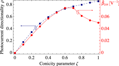
Since the operating frequency range only contains one plasmonic rsonance, the increase in is almost uniform across the spectrum. We can thus introduce an overall spectrally averaged for the structure with a given the resulting dependence is shown in Fig. 4. We can see that highly asymmetric nanoparticles () display significant that exceeds 0.5, while for fully conical nanoparticles .
Moreover, we see that the field enhancement also becomes greater when particles become more asymmetric, with maximum changing from about 40 for cylinders to almost 100 for cones. Using Eq. (10) and the expression for for Au/GaAs interface calculated in ourTammBulk at the maximum of the dependence (see Fig. 3a), we can finally derive the effective tensor component , also shown in Fig. 4. We see that the maximum value of around 0.07 is reached for conicity parameter values (Fig. 4). For more asymmetric shapes, the increase in and is compensated by the shift of plasmonic resonance towards , where rapidly approaches zero, leading to a slight decrease in to values around 0.05. Changing the nanoparticle’s aspect ratio in such a way that its plasmonic resonance gets shifted to higher frequencies (exceeding 1 eV) is expected to counteract this effect and further boost the directional photocurrent.
The resulting values of in Fig. 4 are seen to greatly exceed the typical values for ferroelectric crystals such as the experimentally determined in bulkFridkinBatirov . The obtained is also found to exceed the anomalously high values for bismuth ferrite known to outperform typical ferroelectric materials by about five orders of magnitude in the thin-film configuration ( around according to the recent measurements bulkBiFe and first-principle theoretical calculations bulkYoungPRL ). Furthermore, it exceeds the values calculated for the photogalvanic effect based on ratchet photocurrent from interaction of free electrons with asymmetric nanoscatterers without taking any plasmonic effects into consideration galvPhysE .
Hence, the plasmonic photogalvanic effect in metamaterials based on asymmetrically shaped nanoparticles can be confirmed to constitute a “giant” version of bulk photovoltaic effect present in non-centrosymmetric crystals.
IV Plasmonic versus conventional photogalvanic effect
Having established formal equivalence between the conventional bulk photovoltaic effect in non-centrosymmetric crystalline materials Fridkin2001 and the reported plasmonic effect in nanoparticles through the parallels between Eqs. (8) and (7), or similarly between Eqs. (9) and (10), we would like to discuss the similarities in the underlying physics behind these two effects in more detail.
Conventional photogalvanic effect galvUFN or bulk photovoltaic effect Fridkin2001 (sometimes called high-voltage bulk photovoltaic effect bulkGlass ) refers to the generation of intrinsic photocurrents occurring in single-phase materials without inversion symmetry bulkYoungPRL1 . Microscopically, it is associated with violation of the principle of detailed balance for photoexcited non-equilibrium carriers in noncentrosymmetric crystals: the probability of the electron transition between the states with momentum and , , does not, in general, equal the probability of the reverse transition: galvIOP . This gives rise to a flux of photoexcited carriers, which manifests itself as photocurrent with a certain direction even though the medium is homogeneous and uniformly illuminated.
The principle of detailed balance may be violated due to a variety of mechanisms, e.g., inelastic scattering of carriers on non-centrosymmetric centers, excitation of impurity centers with an asymmetric potential, or hopping mechanism that acts between asymmetrically distributed centers Fridkin2001 . Other effects that have been pointed out are excitation of non-thermalized electrons having asymmetric momentum distribution due to crystal asymmetry, delocalized optical transitions in lattice excitation of pyroelectrics bulkGlass , spin-orbital splitting of the valence band in gyrotropic media Fridkin2001 , and second-order nonlinear optical interaction known as “shift currents”, shown to be the dominating photocurrent cause in ferroelectrics bulkYoungPRL ; bulkYoungPRL1 .
The latter effect is strikingly similar to the plasmonic effect reported here because the expression for the “shift current”, , is essentially coincident with Eqs. (7)–(8); in both cases, the photocurrent is quadratic with respect to the field strength of incident light plas5-UskovUFN12 .
Another striking similarity arises when one compares the considered photoemission from nanoparticles with photoionization from atoms. Indeed, one can regard nanoparticles as atoms whose electrons are placed into a highly asymmetric potential well, which is formed by the boundary of metal with the surrounding medium. Then, it is known from atomic physics that the pattern of photoeffect from such atoms would depend on the shape of the atomic potential well. From this point of view, it is clear that changing the shape of the nanoparticles can efficiently deform the pattern of electron photoemission from such nanoparticles in much the same way as what happens in non-centrosymmetric crystals where asymmetry is inherent in the crystal lattice structure.
Hence, we have solid grounds to regard the reported plasmonic effect in nanoparticle arrangements as the plasmonic analogy (or “metamaterial counterpart”) to the conventional photogalvanic or bulk photovoltaic effect, if we think of nanoparticles as “meta-atoms” and equate the absence of the center of symmetry in them to a similar geometric feature of crystal lattice in bulk media. In some ways, it resembles the mesoscopic photovoltaic effect that was reported earlier to occur in ensembles of semiconductor microjunctions of larger dimensions (about ) in the microwave range meso1JETP ; meso2PRB .
Choosing between the terms photogalvanic and bulk photovoltaic to name the reported effect is worth another discussion. In homogeneous media, these two terms are essentially synonymous and have been used interchangeably. Indeed, historically the words “galvanic” and “voltaic”, attributed to Luigi Galvani and Alessandro Volta respectively (both of whom were behind the invention of a battery), have the same meaning. In later use, though, the term photovoltaic effect gained a much wider recognition and at the same time, became much more generic; it came to mean any effect of electric energy generation as a result of light illumination (perhaps with the exception of photoelectron emission into vacuum, for which the term photoelectric effect remains more popular). Still, the predominant usage realm of photovoltaic effects became that of the processes in the modern-day semiconductor solar cells, i.e., the effects related to generation and subsequent separation of electrons and holes in semiconductor structures. To distinguish these heterostructure effects from photocurrent generation in the bulk of a non-centrosymmetric homogeneous medium, the latter adopted the name “bulk photovoltaic effect”; its much less popular synonym “photogalvanic effect” has not needed this addition.
For this reason, in our attempt to classify the predicted plasmonic effect, adopting the name “plasmonic bulk photovoltaic effect” can be confusing because one is tempted to forget that a plasmonic metamaterial is only “effectively bulk” in the sense that a macroscopic excitation such as an incident plane wave will not discriminate the individual nanoparticles and will interact with the metamaterial as if it were homogeneous. Microscopically, though, it is not homogeneous; the very existence of localized surface plasmon excitations imply that there are surfaces that give rise to them. The wording “bulk plasmonic photovoltaic effect” would be even more dangerous because it may mislead one into thinking that bulk plasmons, rather than surface plasmons, are at work, which is not the case. Therefore, to avoid such confusions, we argue that plasmonic photogalvanic effect is the proper name for the reported phenomenon.
In the broader picture, it has attributes of both a bulk effect and a surface effect depending on the length scale, and in this way it bridges the gap between the inner photoelectric effect (defined as electric charge carrier generation due to photon absorption in a bulk material) and the outer photoelectric effect (defined as electric charge carrier emission from one medium into another across an interface) bookInnerOuter ; this is not to be confused with internal vs. external photoelectric effect, both of which are subclasses of the outer photoelectric effect depending on whether the second medium is solid or not bookInternalExternal .
One does need to keep in mind, however, that the present numerical demonstration of plasmonic photogalvanic effect, based on a 2D arrangement of nanoparticles, has only succeeded in demonstrating the equivalence for a “thin slab” of metamaterial, analogous to a thin film of a bulk non-centrosymmetric crystalline medium. Further comparison of plasmonic and conventional photogalvanic effect involving a 3D arrangement of nanoparticles should therefore be forthcoming. It is rather straightforward, the key challenge being the means to provide uniform illumination in a medium with sufficiently many lossy metallic inclusions under the condition of localized plasmonic resonance (and hence, highly inhomogeneous and strongly enhanced local fields). Overcoming this challenge may result in a cap on the maximum nanoparticle density and therefore, in a limit on how strong plasmonic photogalvanic effect can be.
That said, the results presented in the numerical demonstration in Section III point out that in terms of the relevant tensor components, plasmonic photogalvanic effect can be several orders of magnitude stronger than the conventional one. Hence, calling the effect giant plasmonic photogalvanic effect is warranted, on par with giant magnetooptical effects present in chiral metamaterials and similarly surpassing the naturally occurring chirality in bulk media by orders of magnitude GiantGyro .
V Conclusions and outlook
To summarize, we have theoretically predicted new functionality in photoconductive metamaterials: the giant plasmonic photogalvanic effect, analogous to photogalvanic (or bulk photovoltaic) effect in homogeneous non-centrosymmetric media bookSturmanFridkin . The reported effect is numerically demonstrated in a metamaterial containing similarly oriented non-centrosymmetric metallic nanoparticles embedded in a homogeneous semiconductor matrix, when illuminated by a wave with photon energies insufficient for the internal photoelectric excitation in the semiconductor. Due to the lower degree of symmetry in the nanoparticles (the absence of mirror symmetry in the - plane), the flux of “hot” electrons emitted from the nanoparticles with the assistance of a resonant plasmonic excitation aquires directionality. Averaged over the volume of the metamaterial, this directionality is manifest as an electromotive force resulting from homogeneous external light illumination (the photogalvanic effect).
We have also found that the resulting current density generated in a layer of nanoparticles grows as the particle shape changes from cylindrical to conical. Furthermore, we have calculated the component of the effective third-rank tensor that relates the induced current density to the incident electric field intensity [see Eq. (10)]. We have shown that the effective for the nanoparticle array exceeds the components for the naturally occurring ferroelectrics with bulk photovoltaic effect bulkBiFe ; bulkYoungPRL ; bulkFridkinBatirov by orders of magnitude. Hence, the reported plasmonic effect can be regarded as a “giant” version of the photogalvanic effect occurring in natural materials, adding to the assortment of effects that are much stronger in artificial metamaterials than in natural media.
On a fundamental level, the proposed effect is important for our understanding of plasmon-assisted electron photoemission processes, and constitutes a new way of exploring light-matter interaction at the mesoscopic scale. On a more applied level, our results can be used in a variety of ways, from a new way of characterizing plasmonic structures (distinct from purely optical or electron-microscopy approaches), to new designs of photodetectors operating outside of the spectral range for band-to-band transitions for semiconductors. It can also be used to increase the performance of photovoltaic elements by making use of longer-wavelength photons, which are normally lost in traditional cells based on the inner photoelectric effect uHalasSci11 ; plas8-Novitsky12 . The result that photoemission predominantly occurs at the base of the nanocones makes them particularly appealing for photovoltaic devices where nanoparticles are deposited on a semiconductor substrate.
Moreover, we can regard photoemission in non-centrosymmetric plasmonic nanoantennas as a “ratchet” (Brownian-motor) mechanism ratchetReimann ; ratchetHanggi that works as an optical rectifier or “rectenna” ratchetGreen . The fundamental concept of optical ratchet devices and optical rectennas attracts much attention in recent developments in nanotechnology ratchetAppErman ; ratchetAppSassine ; ratchetAppValev ; ratchetAppHatano .
Finally, we note that we have only considered the plasmonic analogue of the linear bulk photovoltaic effect, since the nanoparticle shape was chosen to be achiral. It is expected that chiral (or planar chiral) nanoparticles would provide the plasmonic analogue to the circular bulk photovoltaic effect bookSturmanFridkin ; bulkFridkinBatirov , described on analogy with Eq. (9) as
| (11) |
Thus, designing plasmonic nanostructures with anomalously high effective is expected to result in new ways to characterize both chiral plasmonic nanostructures and chirality-related properties of light.
Acknowledgements.
The authors would like to thank Jesper Mørk for valuable comments. S.V.Z. acknowledges support from the People Programme (Marie Curie Actions) of the European Union’s 7th Framework Programme FP7-PEOPLE-2011-IIF under REA grant agreement No. 302009 (Project HyPHONE). V.E.B. acknowledges support from SPIE Optics and Photonics Education Scholarship, as well as Otto Mønsteds and Kaj og Hermilla Ostenfeld foundations. I.E.P. and A.V.U. acknowledge support from the Russian MSE State Contract N14.527.11.0002 and from the CASE project (Denmark).References
- (1) W. Cai and V. M. Shalaev, Optical Metamaterials: Fundamentals and Applications (Springer, 2009).
- (2) V. M. Shalaev, “Optical negative-index metamaterials,” Nature Photon. 1, 41–48 (2007).
- (3) Z. Li, “Chiral metamaterials: from optical activity and negative refractive index to asymmetric transmission,” J. Opt. 15(2), 023001 (2013).
- (4) A. Poddubny, I. Iorsh, P. Belov, and Yu. Kivshar, “Hyperbolic metamaterials,” Nature Photon. 7, 948–957 (2013).
- (5) P. Biagioni, J. Huang, and B. Hecht, “Nanoantennas for visible and infrared radiation,” Rep. Prog. Phys. 75(2), 024402 (2012).
- (6) M. W. Knight, Y. Wang, A. S. Urban, A. Sobhani, B. Y. Zheng, P. Nordlander, and N. J. Halas, “Embedding plasmonic nanostructure diodes enhances hot electron emission,” Nano Lett. 13(4), 1687–1692 (2013).
- (7) A. Sobhani, M. W. Knight, Y. Wang, B. Zheng, N. S. King, L. V. Brown, Z. Fang, P. Nordlander, and N. J. Halas, “Narrowband photodetection in the near-infrared with a plasmon-induced hot electron device,” Nature Commun. 4, 1643 (2013).
- (8) S. V. Zhukovsky, V. E. Babicheva, A. V. Uskov, I. E. Protsenko, and A. V. Lavrinenko, “Enhanced electron photoemission by collective lattice resonances in plasmonic nanoparticle-array photodetectors and solar cells,” Plasmonics, in press, doi: 10.1007/s11468-013-9621-z (2013).
- (9) A. O. Govorov, H. Zhang, and Y. K. Gun’ko, “Theory of photoinjection of hot plasmonic carriers from metal nanostructures into semiconductors and surface molecules,” J. Phys. Chem. 117(32), 16616–16631 (2003).
- (10) H. Chalabi and M. Brongersma, “Plasmonics: Harvest season for hot electrons,” Nature Nanotechnology, 8, 229–230 (2013).
- (11) Y. Nishijima, K. Ueno, Y. Yokota, Kei Murakoshi, and H. Misawa, “Plasmon-assisted photocurrent generation from visible to near-infrared wavelength using a Au-nanorods/ electrode,” J. Phys. Chem. Lett., 1(13), 2031–2036 (2010).
- (12) Y. Takahashi and T. Tatsuma, “Solid state photovoltaic cells based on localized surface plasmon-induced charge separation,” Appl. Phys. Lett., 99(18), 182110 (2011).
- (13) M. W. Knight, H. Sobhani, P. Nordlander, and N. J. Halas, “Photodetection with active optical antennas,” Science 332(6030), 702–704 (2011).
- (14) E. Moulin, U. Paetzold, B. Pieters, W. Reetz, and R. Carius, “Plasmon-induced photoexcitation of “hot” electrons and “hot” holes in amorphous silicon photosensitive devices containing silver nanoparticles,” J. Appl. Phys. 113(14), 144501 (2013).
- (15) T. P. White and K. R. Catchpole, “Plasmon-enhanced internal photoemission for photovoltaics: Theoretical efficiency limits,” Appl. Phys. Lett. 101(7), 073905 (2012).
- (16) S. Mubeen, J. Lee, N. Singh, S. Krämer, G. D. Stucky, and M. Moskovits, “An autonomous photosynthetic device in which all charge carriers derive from surface plasmons,” Nature Nanotechnol. 8, 247–251 (2013).
- (17) I. E. Protsenko and A. V. Uskov, “Photoemission from metal nanoparticles,” Phys. Usp. 55(5), 508–518 (2012).
- (18) A. Novitsky, A.V. Uskov, C. Gritti, I.E. Protsenko, B.E. Kardynał, and A.V. Lavrinenko, “Photon absorption and photocurrent in solar cells below semiconductor bandgap due to electron photoemission from plasmonic nanoantennas,” Prog. Photovolt.: Res. Appl. 22(4), 422–426 (2014).
- (19) A. J. Leenheer, P. Narang, N. S. Lewis, and H. A. Atwater, “Solar energy conversion via hot electron internal photoemission in metallic nanostructures: Efficiency estimates,” J. Appl. Phys. 115, 134301 (2014).
- (20) M. Sun, H. Xu, “A novel application of plasmonics: Plasmon-driven surface-catalyzed reactions,” Small 8, 2777 (2012).
- (21) Y. Liu, H. Zhai, F. Guo, N. Huang, W. Sun, C. Bu, T. Peng, J. Yuan, and X. Zhao, “Synergistic effect of surface plasmon resonance and constructed hierarchical spheres for Dye-Sensitized Solar Cells,” Nanoscale 4, 6863–6869 (2012).
- (22) N. Liu, H. Wei, J. Li, Z. Wang, X. Tian, A. Pan, and H. Xu, “Plasmonic amplification with ultra-high optical gain at room temperature,” Sci. Rep. 3, 1967 (2013).
- (23) B. I. Sturman and V. M. Fridkin, The Photovoltaic and Photorefractive Effects in Noncentrosymmetric Materials (Gordon and Breach, Philadelphia, 1992).
- (24) I. Tamm and S. Schubin, “Zur Theorie des Photoeffektes an Metallen,” Zeitschrift für Physik 68(1–2), 97–113 (1931).
- (25) A.M. Brodsky and Y.Y. Gurevich, Theory of Electron Emission from Metals (Nauka, Moscow, 1973).
- (26) A. Brodsky and Y. Gurevich, “Theory of external photoeffect from the surface of a metal,” Sov. Phys. JETP 27, 114 (1968).
- (27) C. Scales and P. Berini, “Thin-film Schottky barrier photodetector models,” IEEE J. Quant. Electron. 46(5), 633–643 (2010).
- (28) A. V. Uskov, I. E. Protsenko, R. Sh. Ikhsanov, V. E. Babicheva, S. V. Zhukovsky, A. V. Lavrinenko, E. P. O’Reilly, and H. Xu, “Internal photoemission from plasmonic nanoparticles: Comparison between surface and volume photoelectric effects,” Nanoscale 6(9), 4716–4727 (2014).
- (29) S. V. Zhukovsky, V. E. Babicheva, A. V. Uskov, I. E. Protsenko, and A. V. Lavrinenko, “Electron photoemission in plasmonic nanoparticle arrays: Analysis of collective resonances and embedding effects,” to appear in Appl. Phys. A, http://arxiv.org/abs/1308.3345 (2013).
- (30) V. M. Fridkin, “Bulk photovoltaic effect in noncentrosymmetric crystals,” Crystalography Reports 46(4), 722–726 (2001).
- (31) A. D. Chepelianskii, M. V. Entin, L. I. Magarill, and D. L. Shepelyansky, “Theory of photogalvanic effect in asymmetric nanostructures arrays,” Physica E 1264–1266 (2008).
- (32) S. M. Young, F. Zheng, and A. M. Rappe, “First-principles calculation of the bulk photovoltaic effect in bismuth ferrite,” Phys. Rev. Lett. 109, 236601 (2012).
- (33) T. M. Batirov, K. A. Verkhovskaya, R. K. Dzhalalov, E. V. Dubovik, B. V. Mill, and V. M. Fridkin, “Bulk photovoltaic and photorefractive effects in a piezoelectric crystal,” Crystalography Reports 45(1), 154–156 (2000).
- (34) A. M. Glass, D. von der Linde, and T. J. Negran, “High-voltage bulk photovoltaic effect and the photorefractive process in ,” Appl. Phys. Lett. 25(4), 233 (1974).
- (35) V. Ferry, J. Munday, and H. Atwater, “Design considerations for plasmonic photovoltaics,” Adv. Mater. 22, 4794 (2010).
- (36) H. A. Atwater and A. Polman, “Plasmonics for improved photovoltaic devices,” Nature Mater. 9, 205–213 (2010).
- (37) K. Nakayama, K. Tanabe, and H. A. Atwater, “Plasmonic nanoparticle enhanced light absorption in GaAs solar cells,” Appl. Phys. Lett. 93, 121904 (2008).
- (38) A. Kirkeminde, M. Retsch, Q. Wang, G. Xu, R. Hui, J. Wud, and S. Ren, “Surface-passivated plasmonic nano-pyramids for bulk heterojunction solar cell photocurrent enhancement,” Nanoscale 4, 4421 (2012).
- (39) J. Henzie, J. Lee, M. H. Lee, W. Hasan, and T. W. Odom, “Nanofabrication of plasmonic structures,” Annu. Rev. Phys. Chem. 60, 147–165 (2009).
- (40) A. Ordal, R. J. Bell, R. A. Alexander Jr, L. L. Long, and M. R. Querry, “Optical properties of fourteen metals in the infrared and far infrared: Al, Co, Cu, Au, Fe, Pb, Mo, Ni, Pd, Pt, Ag, Ti, V, and W,” Appl. Opt. 24(24), 4493–4499 (1985).
- (41) A. B. Evlyukhin, C. Reinhardt, and B. N. Chichkov, “Multipole light scattering by nonspherical nanoparticles in the discrete dipole approximation,” Phys Rev. B 84, 235429 (2011).
- (42) A. B. Evlyukhin, C. Reinhardt, E. Evlyukhin, and B. N. Chichkov, “Multipole analysis of light scattering by arbitrary-shaped nanoparticles on a plane surface,” J. Opt. Soc. Am. B 30, 2589–2598 (2013).
- (43) K. Kelly, E. Coronado, L. Zhao, and G. Schatz, “The optical properties of metal nanoparticles: The influence of size, shape, and dielectric environment,” J. Phys. Chem. B 107, 668 (2003).
- (44) W. Ji, K. Yao, and Y. C. Liang, “Evidence of bulk photovoltaic effect and large tensor coefficient in ferroelectric thin films,” Phys. Rev. B 84, 094115 (2011).
- (45) V. Belinicher, B. Sturman, “The photogalvanic effect in media lacking a center of symmetry,” Sov. Phys. Usp. 23, 199 (1980).
- (46) G. Chanussot and A. M. Glass, “A bulk photovoltaic effect due to electron-phonon coupling in polar crystals,” Phys. Lett. A 59(5), 405–407 (1976).
- (47) S. M. Young and A. M. Rappe, “First principles calculation of the shift current photovoltaic effect in ferroelectrics,” Phys. Rev. Lett. 109, 116601 (2012).
- (48) A. Grachev, E. Nippolainen, and A. Kamshilin, “Photogalvanic effect induced by an electric field,” New J. Phys. 8, 78 (2006).
- (49) V. I. Fal’ko and D. E. Khmel’nitskii, “Mesoscopic photovoltaic effect in microjunctions,” Sov. Phys. JETP 68, 186 (1989).
- (50) J. Liu, M. A. Pennington, and N. Giordano, “Mesoscopic photovoltaic effect,” Phys. Rev. B 45, 1267–1272 (1992).
- (51) F. C. Champion, University Physics, part 5 (Blackie & Sons Ltd., Chicago, 1960), p. 728.
- (52) V. V. Afanas’ev, Internal Photoemission Spectroscopy: Principles and Applications (Elsevier, Oxford, 2008).
- (53) M. Kuwata-Gonokami, N. Saito, Y. Ino, K. Jefimovs, T. Vallius, J. Turunen, and Y. Svirko, “Giant optical activity in quasi-two-dimensional planar nanostructures,” Phys. Rev. Lett. 95, 227401 (2005).
- (54) P. Reimann, “Brownian motors: noisy transport far from equilibrium,” Phys. Rep. 361, 57–265 (2002).
- (55) P. Hänggi, F. Marchesoni, and F. Nori, “Brownian motors,” Ann. Phys. (Leipzig) 14, 51–70 (2005).
- (56) R. Corkish, M. A. Green and T. Puzzer, “Solar energy collection by antennas,” Solar Energy 73(6), 395–401 (2002).
- (57) S. Sassine, Y. Krupko, J. Portal, Z. Kvon, R. Murali, K. Martin, G. Hill, and A. Wieck, “Experimental investigation of the ratchet effect in a two-dimensional electron system with broken spatial inversion symmetry,” Phys. Rev. B 78, 045431 (2008).
- (58) L. Ermann, A. Chepelianskii, and D. Shepelyansky, “Symmetry breaking for ratchet transport in the presence of interactions and a magnetic field,” Phys. Rev. E 87, 022912 (2013).
- (59) V. K. Valev, N. Smisdom, A. V. Silhanek, B. De Clercq, W. Gillijns, M. Ameloot, V. V. Moshchalkov, and T. Verbiest, “Plasmonic ratchet wheels: switching circular dichroism by arranging chiral nanostructures,” Nano Lett. 9(11), 3945 (2009).
- (60) T. Hatano, T. Ishihara, S. G. Tikhodeev, and N. A. Gippius, “Transverse photovoltage induced by circularly polarized light,” Phys. Rev. Lett., 103, 103906 (2009).