Carrier-number fluctuations in the 2-dimensional electron gas at the LaAlO3/SrTiO3 interface
Abstract
The voltage-spectral density of the 2-dimensional electron gas formed at the interface of LaAlO3/SrTiO3 has been thoroughly investigated. The low-frequency component has a clear 1/f behavior with a quadratic bias current dependence, attributed to resistance fluctuations. However, its temperature dependence is inconsistent with the classical Hooge model, based on carrier-mobility fluctuations. The experimental results are, instead, explained in terms of carrier-number fluctuations, due to an excitation-trapping mechanism of the 2-dimensional electron gas.
pacs:
73.20.-r, 72.70.+m, 73.40.-cPolar/non-polar oxide interfaces can host a 2-dimensional electron gas (2DEG).Ohtomo A well-known example is the LaAlO3/SrTiO3 interface (LAO/STO), made by depositing an epitaxial LAO film onto a single-crystal STO with single TiO2-plane termination. LAO/STO interfaces are conducting, provided LAO thickness exceeds the threshold of unit cells.Thiel The properties of LAO/STO heterojunctions have been widely investigated (see, e.g., Refs. Mannhart, and Zubko, ), and it is known that the mobile electrons populate a quantum well, within the STO side of the junction, with a confinement depth of few nanometers.Copie ; Popovic ; Cantoni The conductance band DOS is constituted of three overlapped 3d t2g sub-bands (namely, Ti3dxy, Ti3dxz, and Ti3dyz), with lifted degeneracy due to the breakdown of lattice symmetry imposed by the interface, and populated by charges injected from the donor states. The nature of such donors is still controversial. They are mainly identified either as valence band or in-gap states located at the LAO surface (electronic reconstruction model),Popovic ; Santander ; Berner or as defect states located in STO (models based on cation intermixing or oxygen vacancies).Chambers The electronic conduction can be qualitatively understood in terms of charge carrier of the 2DEG hopping between otherwise empty Ti4+ (i.e., Ti(d0)) sites. Such states are prone to localization, in the presence of either interface disorder, due to their bidimensional nature (Anderson localization), or of a strong coupling with the lattice (polaronic localization),Devreese that might well be attributed to the Jahn-Teller effect taking place in Ti(d1) cations. It has been proposed in Ref. Popovic, that such localization mainly affects the Ti3d states deriving from the interfacial TiO2 layer, and in particular the low-energy Ti3dxy sub-band, while Ti3d states from the very next atomic layers might host mobile electrons.
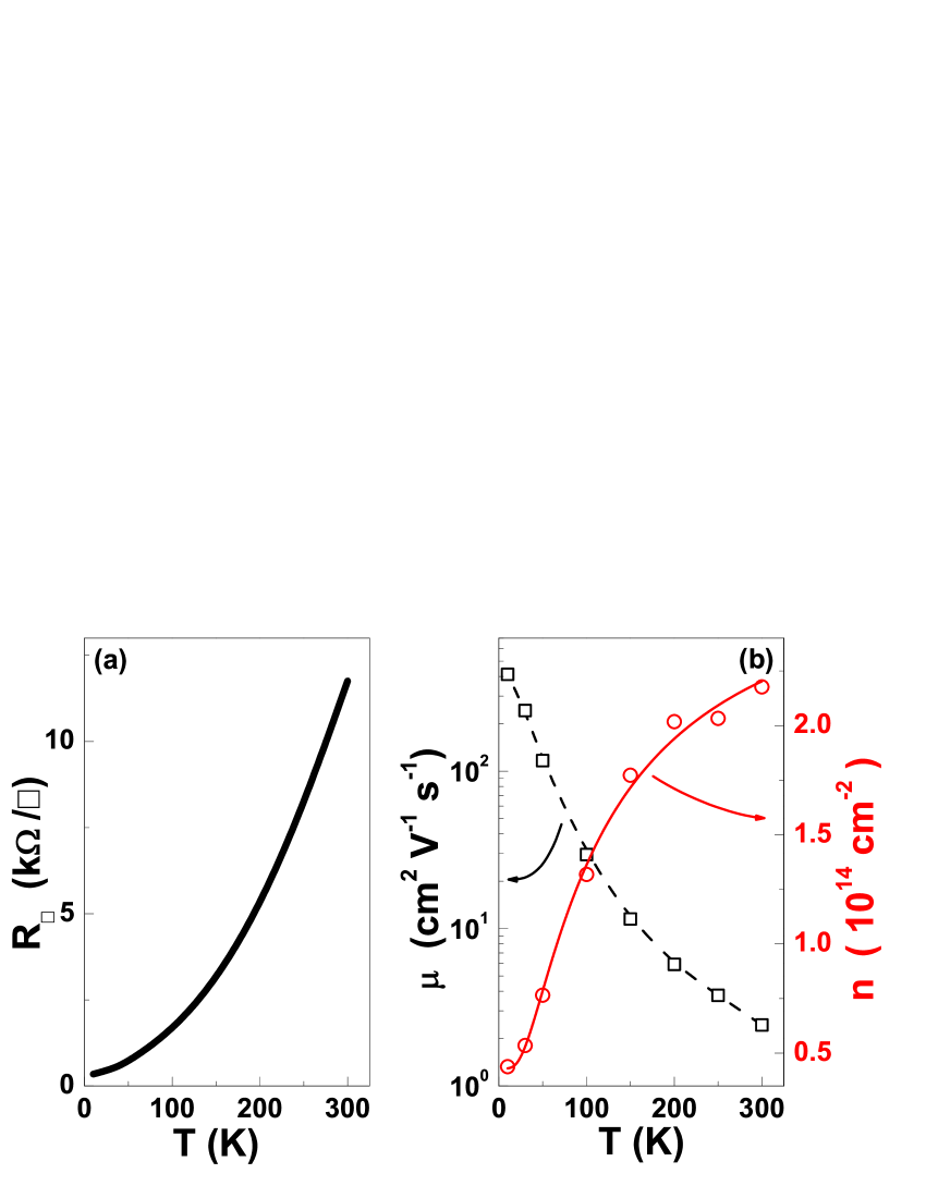
LAO/STO shows a metallic sheet resistance vs. temperature in a wide range of temperature, with typical value k/ at room temperature, that drops to zero at the superconducting transition, normally in the mK range.Caviglia The carrier density and mobility are usually determined from Hall effect and magnetoresistance measurements, including the observation of Schubnikov-De Haas oscillations.Caviglia2 In particular, the 2DEG charge carrier density ranges from to cm-2, depending on the fabrication conditions, with a sensitive variation on temperature (see, e.g., Ref. Dubroka, ). The mobility is also affected by the fabrication process; typical values are about cm2V-1 at room temperature and reach up to cm2V-1 at low temperature. As a general phenomenological trend, the lower is the charge carrier density, the higher the mobility.Huijben
In view of the possible applications of LAO/STO based devices, it is important to characterize the transport properties by also addressing the intrinsic electric noise. Noise in semiconductors has been deeply investigated;2DEG-Semic while, besides a few seminal works on the subject, the electric noise in conducting oxides remains a young and stimulating field of research, still open to both theoretical and experimental activity.MangaNoise The so-called ”electric noise spectroscopy” has already demonstrated good potential for the comprehension of non conventional transport phenomena in oxides (see, e.g., Refs. Barone-LSMO, ; Barone-PCMO, ; Barone-WL, ). It may, therefore, contribute to clarify still unsolved fundamental questions regarding the electronic properties of LAO/STO.
A detailed characterization and interpretation of the noise spectral density in LAO/STO interface is here reported. The samples were fabricated by RHEED-assisted laser ablation, following standard procedures described in Ref. Napoli-Interfaces, , giving sharp, high quality structures,Cantoni and reproducible transport properties.DiGennaro Au wires were bonded to the samples by ultrasonic bonder in the standard four-probe Van der Pauw geometry. and Hall effect measurements were carried out on a batch of samples in a He-flux cryostat from K to room temperature and in magnetic fields up to T. Resistance and I-V curves were measured both in constant and pulsed mode. Current values from to mA were used, in order to rule out Joule-heating effects. Noise measurements were made in a closed-cycle refrigerator at temperatures between and K, with a stability better than K. A low-noise digital current supply was used for biasing the samples. The output voltage signal, amplified with a low-noise PAR5113 preamplifier, was acquired by dynamic signal analyzer HP35670A. The equivalent input voltage-spectral density, due to the electronic chain, was typically V2/Hz. A specific experimental procedure, described in detail in Ref. Barone-NoiseRed, , was applied to minimize the electrical noise generated by the contacts.
In the following the data from a representative LAO/STO sample with unit cells thick LAO film grown on STO substrate at ∘C in an oxygen pressure mbar are reported. The sheet resistance is shown in Fig. 1(a); the carrier density and the mobility (as deduced by Hall effect measurements in a single band approximation) are shown in Fig. 1(b). The temperature dependence of the carrier density can be satisfactorily described by (see the solid line in Fig. 1(b))
| (1) |
where and are mobile and trapped charge carriers, respectively. The best fitting parameters are cm-2, cm-2, meV. From Eq. (1), at the conduction band is populated with charge carriers, while are trapped in a very narrow band at energy below the chemical potential . These trapped states may be interpreted as large polarons or as Anderson-localized states. The thermal activation of localized electrons promotes a consistent number of carriers to the mobile states, and explains the strong temperature dependence of seen by the Hall effect measurements. In this context, the total number of electrons in the quantum well is given by .
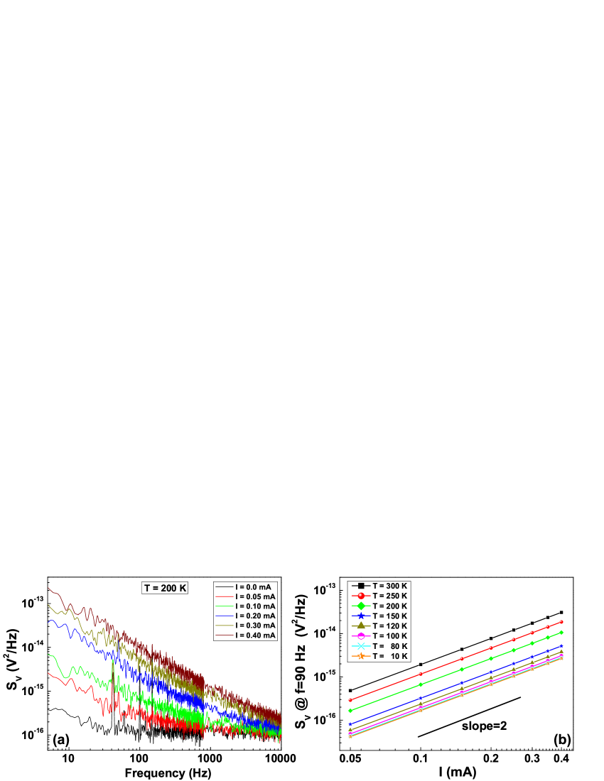
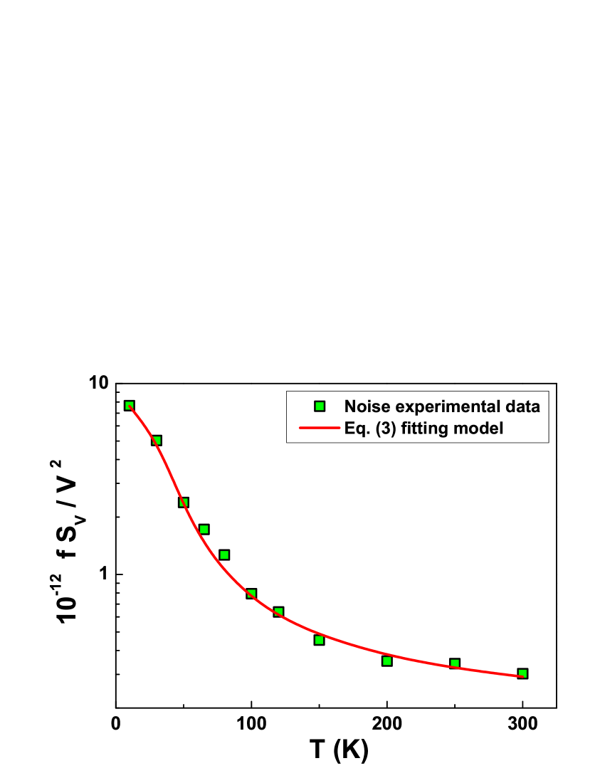
In Fig. 2(a) the spectral noise measured at K is shown for different bias currents. At all temperatures, the frequency dependence of the spectral traces is characterized by a pure 1/f behavior (Flicker noise)1/fNote at low frequencies, while, at higher frequency, tends to a constant value. The latter being the sum of the Johnson noise , and the background readout electronic noise. The sharp peaks in the spectra are a spurious effect, due to coupling to external noise sources and are excluded from the noise analysis. The dependence of on the bias current is shown in Fig. 2(b) and is quadratic in the whole temperature range, with an exponent . This is a clear indication that the 1/f noise is generated by resistance fluctuations.Kogan It is, therefore, possible to define a ”normalized noise level”, i.e., the product , that is a function of the temperature only, as shown in Fig. 3.
By standard statistics it is obtained
| (2) |
where , , and are the variances of the sample resistance , of the total carrier number (with , being the effective sample area), and of the electron mobility , respectively. The relation in Eq. (2) highlights two possible sources of resistance fluctuations, i.e., carrier-number fluctuations and mobility fluctuations. The latter is always dominating in metals. In the high-frequency range, is mainly determined by the thermal fluctuations of the mean free path, leading to the Johnson white noise. At low frequencies, the statistical variance of the mean free path dominates. The mobility is connected to the ensemble average of the mean free path; therefore, its variance follows the scaling law . The phenomenological Hooge formula captures this concept; the Flicker noise level due to mobility fluctuations is then given by , with .Kogan The results for LAO/STO do not follow this behavior. The data, instead, are very well fitted by
| (3) |
where is the total carrier density given by Eq. (1). This implies that the noise level scales with the inverse square of the mobile carrier number. The red solid curve in Fig. 3 is the plot of the function in Eq. (3), with cm-4. In consideration of Eq. (2), these results on LAO/STO are interpreted as indicative of carrier-number fluctuations.
A similar behavior has been described by McWhorter,McWhorter and observed in semiconducting structures hosting a 2DEG.Noise-Semic In this work, the model of carrier-number fluctuations has been developed for LAO/STO 2DEG to explain both the 1/f dependence, and the dependence of . The full details of the model derivation are reported as Supplemental Material (see Ref. SuppMat, ). The main assumptions are given in the following, together with the outline of the mathematical procedure.
Referring to Eq. (1), due to the stochastic processes of excitation-trapping, the number of mobile electrons deviates from its equilibrium value. This process is described by the function , that satisfies the rate equation
| (4) |
where is an uncorrelated noise generator, and is the characteristic time for the equilibration of mobile electrons with traps. After some manipulations,SuppMat from Eq. (4) it is possible to obtain the Fourier transform of , , and the spectral noise density as
| (5) |
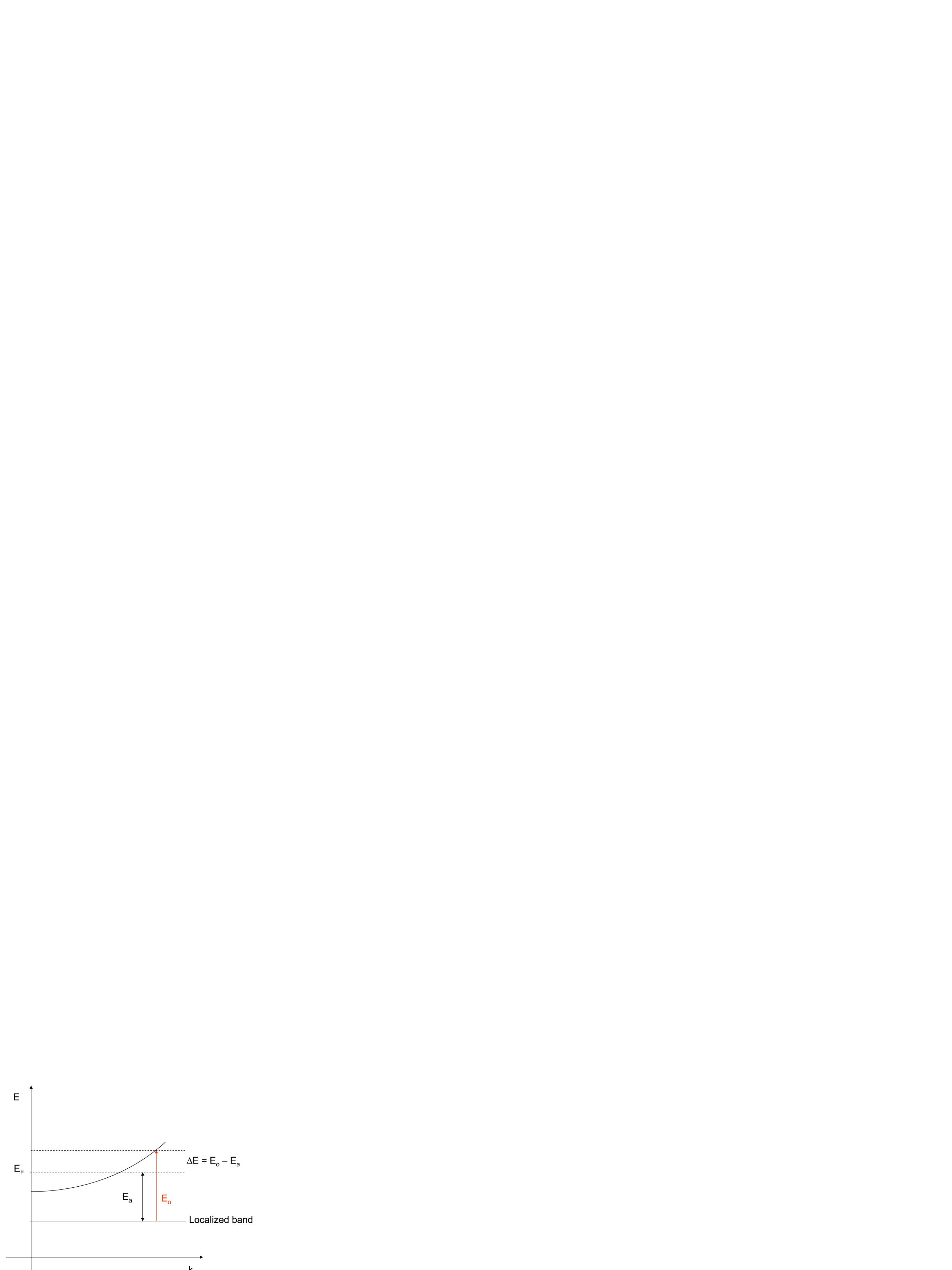
where , and is the variance on the stochastic variable . In order to determine , the mechanism of excitation-trapping in oxides has to be considered. It is assumed that the excitation from a trap is mainly due to scattering with acoustic phonons, which carry negligible moment (i.e., it is vertical in the k-space). According to the sketch in Fig. 4, such process requires an activation energy , which is supposed to be uniformly distributed above the threshold . Therefore, when substituting in Eq. (5) and summing over , it is obtained: . Recalling that , the normalized voltage-spectral density is derived as
| (6) |
Equation (6) is the same expression as Eq. (3), where is identified with the temperature-independent variance . A more refined calculation of , reported in Ref. SuppMat, , shows that indeed its temperature dependence is very weak. As a final comment, the noise behavior of the LAO/STO samples studied here is significantly different from that of doped STO.Guerrero In the latter case the noise level does not scale with the inverse square of carriers number. However, doped STO shows a very high mobility, indicating the suppression of electron self-trapping; hence, it is reasonable to infer that the noise generation in STO depends on mobility fluctuations rather than on carrier-number fluctuations.
In conclusion, transport properties of LAO/STO interface have been characterized in detail by Hall effect and spectral noise measurements. The experimental findings support the existence of a thermally activated mechanism which promotes charge carriers from a narrow, underlying band (attributed to polarons or to Anderson-localized states), to the conduction band. The low-frequency Flicker noise spectra have pure 1/f dependence, with a scaling, allowing the attribution of the noise to resistance fluctuations. The noise level dependence on temperature cannot be consistently explained in terms of the classical Hooge picture. It is, instead, shown that a model based on the fluctuation of the carrier number describes correctly the experimental observations.
References
- (1) A. Ohtomo, H. Y. Hwang, Nature 427, 423 (2004).
- (2) S. Thiel, G. Hammerl, A. Schmehl, C. W. Schneider, and J. Mannhart, Science 313, 1942 (2006).
- (3) J. Mannhart, D. H. A. Blank, H. Y. Hwang, A. J. Millis, and J.-M. Triscone, MRS Bulletin 33, 1027 (2008).
- (4) P. Zubko, S. Gariglio, M. Gabay, P. Ghosez, and J.-M. Triscone, Annu. Rev. Cond. Mat. Phys. 2, 141 (2011).
- (5) O. Copie, V. Garcia, C. Bödefeld, C. Carrétéro, M. Bibes, G. Herranz, E. Jacquet, J.-L. Maurice, B. Vinter, S. Fusil, K. Bouzehouane, H. Jaffrès, and A. Barthélémy, Phys. Rev. Lett. 102, 216804 (2009).
- (6) Z. S. Popović, S. Satpathy, and R. M. Martin, Phys. Rev. Lett. 101, 256801 (2008).
- (7) C. Cantoni, J. Gazquez, F. Miletto Granozio, M. P. Oxley, M. Varela, A. R. Lupini, S. J. Pennycook, C. Aruta, U. Scotti di Uccio, P. Perna, and D. Maccariello, Adv. Mater. 24, 3952 (2012).
- (8) A. F. Santander-Syro, O. Copie, T. Kondo, F. Fortuna, S. Pailhès, R. Weht, X. G. Qiu, F. Bertran, A. Nicolaou, A. Taleb-Ibrahimi, P. Le Fèvre, G. Herranz, M. Bibes, N. Reyren, Y. Apertet, P. Lecoeur, A. Barthélémy, and M. J. Rozenberg, Nature 469, 189 (2011).
- (9) G. Berner, M. Sing, H. Fujiwara, A. Yasui, Y. Saitoh, A. Yamasaki, Y. Nishitani, A. Sekiyama, N. Pavlenko, T. Kopp, C. Richter, J. Mannhart, S. Suga, and R. Claessen, Phys. Rev. Lett. 110, 247601 (2013).
- (10) S. A. Chambers, Surface Science 605, 1133 (2011).
- (11) J. T. Devreese, S. N. Klimin, J. L. M. van Mechelen, and D. van der Marel, Phys. Rev. B 81, 125119 (2010).
- (12) A. D. Caviglia, S. Gariglio, N. Reyren, D. Jaccard, T. Schneider, M. Gabay, S. Thiel, G. Hammerl, J. Mannhart, and J.-M. Triscone, Nature 456, 624 (2008).
- (13) A. D. Caviglia, S. Gariglio, C. Cancellieri, B. Sacépé, A. Fête, N. Reyren, M. Gabay, A. F. Morpurgo, and J.-M. Triscone, Phys. Rev. Lett. 105, 236802 (2010).
- (14) A. Dubroka, M. Rossle, K. W. Kim, V. K. Malik, L. Schultz, S. Thiel, C. W. Schneider, J. Mannhart, G. Herranz, O. Copie, M. Bibes, A. Barthélémy, and C. Bernhard, Phys. Rev. Lett. 104, 156807 (2010).
- (15) M. Huijben, A. Brinkman, G. Koster, G. Rijnders, H. Hilgenkamp, and D. H. A. Blank, Adv. Mater. 21, 1665 (2009).
- (16) Y. Chen, C. M. Van Vliet, P. M. Koenraad, and G. L. Larkins, Jr., J. Appl. Phys. 86, 6206 (1999); A. Balandin, K. L. Wang, A. Svizhenko, and S. Bandyopadhyay, IEEE Trans. Electron Devices 46, 1240 (1999); A. Matulionis, R. Katilius, J. Liberis, L. Ardaravicius, L. F. Eastman, J. R. Shealy, and J. Smart, J. Appl. Phys. 92, 4490 (2002).
- (17) X. D. Wu, B. Dolgin, G. Jung, V. Markovich, Y. Yuzhelevski, M. Belogolovskii, and Y. M. Mukovskii, Appl. Phys. Lett. 90, 242110 (2007); L. Méchin, J.-M. Routoure, S. Mercone, F. Yang, S. Flament, and R. A. Chakalov, J. Appl. Phys. 103, 083709 (2008).
- (18) C. Barone, C. Adamo, A. Galdi, P. Orgiani, A. Yu. Petrov, O. Quaranta, L. Maritato, and S. Pagano, Phys. Rev. B 75, 174431 (2007).
- (19) C. Barone, A. Galdi, N. Lampis, L. Maritato, F. Miletto Granozio, S. Pagano, P. Perna, M. Radovic, and U. Scotti di Uccio, Phys. Rev. B 80, 115128 (2009).
- (20) C. Barone, F. Romeo, A. Galdi, P. Orgiani, L. Maritato, A. Guarino, A. Nigro, and S. Pagano, Phys. Rev. B 87, 245113 (2013).
- (21) P. Perna, D. Maccariello, M. Radovic, U. Scotti di Uccio, I. Pallecchi, M. Codda, D. Marré, C. Cantoni, J. Gazquez, M. Varela, S. J. Pennycook, and F. Miletto Granozio, Appl. Phys. Lett. 97, 152111 (2010); C. Aruta, S. Amoruso, R. Bruzzese, X. Wang, D. Maccariello, F. Miletto Granozio, and U. Scotti di Uccio, Appl. Phys. Lett. 97, 252105 (2010); S. Amoruso, C. Aruta, R. Bruzzese, X. Wang, and U. Scotti di Uccio, Appl. Phys. Lett. 98, 101501 (2011); C. Aruta, S. Amoruso, G. Ausanio, R. Bruzzese, E. Di Gennaro, M. Lanzano, F. Miletto Granozio, M. Riaz, A. Sambri, U. Scotti di Uccio, and X. Wang, Appl. Phys. Lett. 101, 031602 (2012).
- (22) E. Di Gennaro, U. Scotti di Uccio, C. Aruta, C. Cantoni, A. Gadaleta, A. R. Lupini, D. Maccariello, D. Marré, I. Pallecchi, D. Paparo, P. Perna, M. Riaz, and F. Miletto Granozio, Adv. Opt. Mater., doi: 10.1002/adom.201300150.
- (23) C. Barone, A. Galdi, S. Pagano, O. Quaranta, L. Méchin, J.-M. Routoure, and P. Perna, Rev. Sci. Instrum. 78, 093905 (2007).
- (24) By fitting the low-frequency regions with the function , the best fit value was obtained.
- (25) S. Kogan, Electronic Noise and Fluctuations in Solids (Cambridge University Press, Cambridge, 1996).
- (26) A. L. McWhorter, Semiconductor Surface Physics (University of Philadelphia Press, Philadelphia, 1957).
- (27) S. T. Hsu, D. J. Fitzgerald, and A. S. Grove, Appl. Phys. Lett. 12, 287 (1968); H. E. Maes and S. H. Usmani, J. Appl. Phys. 54, 1937 (1983).
- (28) See Supplemental Material at [URL……] for a detailed description of the mathematical procedures and of the theoretical evaluations performed.
- (29) R. Guerrero, A. Solignac, M. Pannetier-Lecoeur, Y. Apertet, P. Lecoeur, and C. Fermon, Phys. Rev. B 82, 035102 (2010).