Size effects in superconducting thin films coupled to a substrate
Abstract
Recent experimental advances in surface science have made it possible to track the evolution of superconductivity in films as the thickness enters the nanoscale region where it is expected that the substrate plays an important role. Here, we put forward a mean-field, analytically tractable, model that describes size effects in ultrathin films coupled to the substrate. We restrict our study to one-band, crystalline, weakly coupled superconductors with no impurities. The thin-film substrate/vacuum interfaces are described by a simple asymmetric potential well and a finite quasiparticle lifetime. Boundary conditions are chosen to comply with the charge neutrality condition. This model provides a fair description of experimental results in ultrathin lead films: on average, the superconducting gap decreases with thickness and it is always below the bulk value. Clear oscillations, remnants of the shape resonances, are still observed for intermediate thicknesses. For materials with a weaker electron-phonon coupling and negligible disorder, a modest enhancement of superconductivity seems to be feasible. The relaxation of the charge neutrality condition, which is in principle justified in complex oxide heterostructures and other materials, would lead to a much stronger enhancement of superconductivity by size effects.
I Introduction
Research on superconducting thin films has a long tradition in condensed matter physics. In the early 1960s, theoretical mean-field models Thompson and Blatt (1963) predicted oscillations of the superconducting gap and the critical temperature for nanosize film thickness with peaks that greatly exceeded the bulk limit. This nonmonotonic size dependence, usually referred to as shape resonances, has a simple origin. As thickness increases from the two-dimensional limit, new states become eventually available with the quantum numbers of an infinite well of size the thickness of the film. This additional subband enhances superconductivity as the spectral density is proportional to the dimensionless electron-phonon coupling constant. After the first peak, for larger thicknesses, the spectral density decreases until a new subband becomes available and a new peak occurs in the critical temperature.
Initial experimental results in granular thin films of Al Cohen and Abeles (1968) and other materials Kresin and Tavger (1966) also reported a substantial enhancement of the critical temperature with respect to the bulk limit. However, granular materials are intrinsically disordered and impurities suppress shape resonances so a direct relation between theoretical and experimental results was hard to establish.
It was later realized Allen (1975); Yu et al. (1976) that no enhancement is observed in more realistic theoretical models that impose charge neutrality at the interfaces. More refined experiments with smoother films and a better experimental control Jaeger et al. (1989) observed no enhancement of superconductivity but rather a transition at a temperature lower than the bulk mean-field theory prediction.
Recent progresses in nanotechnology and surface science, in particular epitaxial deposition and scanning tunneling microscopy/spectroscopy (STM), have dramatically improved the experimental control in low dimensions, which has led to many exciting results Qin et al. (2009); Zhang et al. (2010); Brun et al. (2009); Bose et al. (2010). For instance, experiments on ultrathin Pb films with thicknesses ranging from a single to a few atomic monolayers Guo et al. (2004); Qin et al. (2009); Zhang et al. (2010) found that superconductivity is still present although weaker than in the bulk limit. Oscillations of the superconducting gap and the critical temperature, below the bulk value, for intermediate thickness, were also reported. Theoretical models proposed to described these results Chen et al. (2006); Shanenko et al. (2007) had free parameters and did not include important features such as the role of the substrate, the finite lifetime of quasiparticles, or an adequate description of the interface. As the thickness decreases, we expect that these features become increasingly important. More detailed first-principles calculations Jia et al. (2006) of the interface in the ultrathin limit do not address superconductivity explicitly. Strikingly, experimental results in oxide interfaces Reyren et al. (2007), and even single- layered iron-based superconductors Liu et al. (2012), exhibit, in some cases, an enhancement of the critical temperature with respect to the bulk limit. The theoretical reasons of this behavior are not yet well understood.
Motivated by these challenges, we put forward a minimal model for ultrathin superconducting films coupled to the substrate which is analytically tractable but that we expect to capture most of the relevant physics without free parameters, except the quasiparticle lifetime. However, we have found that its role is relatively minor at least in STM experiments. A refined model of the film/substrate interface, based on experimental data, would probably account for this parameter, however, this is beyond the scope of the paper.
In order to avoid the intricacies of the Kosterlitz-Thouless transition, we restrict ourselves to the low-temperature limit of weakly coupled one-band superconductor where a mean- field approach is still accurate. The film and the substrate are described by an asymmetric potential well plus a finite quasiparticle lifetime. Charge neutrality is included, although in some cases, such as in complex oxide heterostructures Zubko et al. (2011), it is unclear whether it applies. We note that in these materials, charge spreading across the interface alters boundary conditions at the interfaces leading to an electrostatic binding between the layers that can prevent the charge neutrality condition to hold. Disorder is not considered as the experiments can be carried out in the limit where the effect of impurities is negligible.
We report results for the superconducting gap () at zero temperature as a function of the film thickness for a broad range of the parameters that define the substrate and also for different electron-phonon coupling constants. The dependence of the results on the validity of the charge neutrality condition Yu et al. (1976) is also investigated in detail. On average, the superconducting gap decreases with thickness. However, remnants of the shape resonances are still observed in some range of parameters. For a weak coupling to the substrate, and a weak electron-phonon coupling, a modest enhancement of superconductivity is observed for certain thicknesses even if the charge neutrality condition holds. Much larger enhancement is expected for material in which the charge neutrality condition does not hold. Finally, we show that this theoretical model provides a fair qualitative description of the Pb ultrathin-film experiments mentioned above.
The paper is organized as follows. In the next section, we introduce the microscopic model that describes superconductivity and the asymmetric potential well that, together with the finite lifetime, models the substrate. The model is then solved in Sec. III by a combination of mean-field and semiclassical techniques. Then, we present results of the superconducting gap as a function of the thickness for different values of the parameters. Based on this information, we discuss the range of realistic experimental settings for which it is feasible to observe shape resonance and/or an enhancement of superconductivity and discuss the relevance of these results for recent Pb ultrathin-film experiments.
II Model
We put forward a model for a superconducting thin film coupled to the substrate. Superconductivity is described by a mean-field approach. The substrate is modeled by an asymmet- ric finite well that depends on the difference between the bulk chemical potential of the materials in the film and the substrate. This confinement leads to the quantization of the momentum component perpendicular to the film plane. We also introduce a finite quasiparticle finite lifetime to describe tunneling into the substrate and any other source of decoherence. Charge neutrality is also taken into account to model the interface, but we also present present results without it as we believe that in some materials it might not fully apply. We start with a description of the theoretical model employed to describe superconductivity.
II.1 Mean field approach to superconductivity in thin films
In a finite-size system, the BCS Hamiltonian in terms of a set of good quantum numbers is given by
| (1) |
where is the dimensionless coupling constant, is the system volume, is the mean level spacing [inverse of the spectral density of states at the Fermi energy ()], is the spin index, , are the usual quasiparticle annihilation and creation operators. The interaction matrix elements are where are the three-dimensional quasiparticle eigenfunctions with the eigenstates of the one-dimensional problem in the direction perpendicular to the film.
A mean field approach to the Hamiltonian above leads to the following Bardeen-Cooper-Schrieber (BCS) gap equation at zero temperature,
| (2) |
The sum is restricted to those states such that is inside the Debye window: where is the Debye frequency.
We consider a thin film of lateral size much larger than its thickness. Therefore, the sum in Eq. (2) can be substituted by an integral in the in-plane momentum components, where we imposed periodic boundary conditions, and a finite sum in the perpendicular dimension.
With the previous considerations Eq. (2) leads to the following system of equations for , :
| (3) |
where is the thin-film area, and ( is the film thickness) is obtained after having performed the and integrals in . is the two-dimensional density of states and the in-plane effective mass. The factor asinh comes from the integration in the in-plane momentum components.
Since depends on , Eq. (3) is a system of non-linear equations which leads to a momentum-dependent order parameter, . Assuming that the mean level spacing is much smaller than the bulk gap, we define the superconducting gap as de Gennes (1964) the minimum energy needed to excite quasiparticles, namely . This observable, which is measured by STM and other spectroscopic techniques, is the one that we use to characterize superconductivity in the system. In order to eliminate the momentum dependence of the gap, and further simplify the calculation, we replace by , the highest occupied state. In this way, an approximate solution of Eq. (3) is simply,
| (4) |
In Figs. 3 and 4, we show explicitly that, especially for larger values of the electron-phonon coupling constant, this is a good approximation, namely, . Another reason to use this additional approximation is that the corrections of the superconducting gap induced by a finite quasiparticle lifetime, studied in Sec. II.2.3, can easily be computed from Eq. (4), while a calculation from Eq. (3) is technically very demanding.
II.2 Model of the thin-film coupling to the substrate
The model of the coupling between the thin film and the substrate/vacuum has three ingredients: the effective potential felt by the quasiparticles due to the substrate, the finite quasiparticle lifetime, and the charge neutrality condition.
II.2.1 Effective potential: An asymmetric finite well
The model of an asymmetric finite well has been previously implementedCzoschke et al. (2005) to study the energy spectrum and size effects in nonsuperconducting thin films. We employ the same effective potential felt by the quasiparticles in the thin film as a consequence of the substrate. As is sketched in Fig. 1, the potential has three parameters: the height of the film/substrate interface, the height of the film/vacuum interface, and the film thickness .
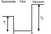
For we take the sum of the ionization level plus the (bulk) Fermi energy of the film material. For we choose the mismatch between and the Fermi energy of the substrate, or conduction band edge (CBE), plus an extra contribution due to the height of a Schottky barrier at the interface. In principle a more complicated potential above the CBE might give better quantitative results. However we stick to a simpler more general approach as a truly realistic potential could result in a time-dependent problem.van Dijk and Nogami (2002) Moreover the exact details of the potential are expected to be sensitive to the substrate material.
Before turning our attention to the solution of the Schrödinger equation in this potential we briefly comment on the dispersion relation and the boundary condition that we have employed.
Dispersion relation. Following previous worksThompson and Blatt (1963) we use a quadratic dispersion relation but with three parameters,
| (5) |
where and determine the position of the band and the effective mass controls the curvature. The motivation for introducing is that it allows to describe a back-folded conduction band (see Fig. 2) in sp metals such as Pb and Al commonly employed in thin-film experiments Guo et al. (2004); Qin et al. (2009); Kirchmann et al. (2010); Zhang et al. (2010); Aballe et al. (2001a).
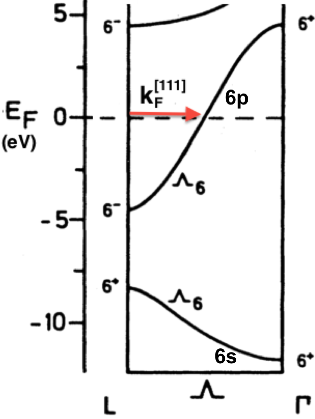
For comparison with experimental results we take that quantization in the momentum-space direction , where and are the crystallographic points corresponding to zero momentum and . This fixes where is the distance between atomic planes in the [111] direction. For a face-centered cubic cell (lattice constant). We do not consider the decrease in the lattice constant at low temperatures. On the other hand (the maximum value of in Eq. (5)) corresponds to the momentum at which the band reaches the Fermi energy. It is such that the Fermi momentum obtained from de Haas-van Alphen experiments equals .
BenDaniel-Duke boundary conditions. As usual, we impose continuity of the wavefunction in both interfaces. For the continuity of the first derivative we consider the effective masses in the film and substrate. These are known as the BenDaniel-Duke boundary conditions, commonly used in heterostructures BenDaniel and Duke (1966),
| (6) |
We have placed the film/substrate interface at and the film/vacuum interface at . We have defined and as the effective masses in the film and substrate, respectively. In the vacuum region, we have taken the free electron mass, .
With the previous considerations, the quantization condition for (the component perpendicular to the film) is
| (7) |
with , , , , and . The total thin-film eigenstates are then given by
| (8) |
where and and , the in-plane momentum components, are subject to periodic boundary conditions.
II.2.2 Charge neutrality
As was mentioned earlier, Dirichlet/rigid boundary conditions at the interfaces, a key ingredient for the observation of large shape resonances, are not consistent Allen (1975) with the principle of charge neutrality in film surfaces. Despite the fact that our boundary conditions allow the eigenstates to extend beyond the interface, with a typical size controlled by the step heights and , charge neutrality is not yet satisfied.
In order to comply with this condition, it was proposed Sugiyama (1960) to extend the potential a distance which is chosen so that surface charge neutrality holds. This shift induces a phase shift, , which together with , the phase shift induced by the potential, must satisfy,
| (9) |
The length is obtained by using Eq. (8) and taking into account that the quantized component of the momentum is ,
| (10) |
As was shown elsewhere Yu et al. (1976), the larger the stronger the average suppression of superconductivity. Once is known, the quantized energy levels and eigenstates are computed for a well of thickness where is the geometrical film thickness. We shall see that the charge neutrality condition also modifies the chemical potential, the matrix elements , and therefore the superconducting energy gap.
Effectively, a finite caused by charge neutrality, amounts to a modification of the boundary conditions. Therefore, it should not change the electron density or the phonon-mediated interaction. We also stress that this approximate method to satisfy charge neutrality is only valid as long as Garcia-Moliner and Flores (1979). Such condition might not be satisfied for films of only a few monolayers (ML) thick. Furthermore, in the film/substrate interface, there is a transition layer (wetting layer) Chan et al. (2003) in which the film atoms are bonded to both the substrate and other atoms of the film. Thus, it is not clear to what extent charge neutrality is applicable in this interface. Moreover, as was mentioned previously, in complex oxide heterostructures Zubko et al. (2011) and other materials, net electric fields in the surface could severely suppress charge neutrality.
II.2.3 Finite lifetime
In this section, we introduce the last ingredient of our model for the coupling of the thin film to the substrate: a finite quasiparticle lifetime. The introduction of a finite quasiparticle lifetime is motivated by the existence of a non-zero probability of tunneling into the substrate. It is also an effective way to account for the realistic potential at the interface and other sources of quasiparticle decoherence, such as inelastic scattering. We shall see that it also plays an important role in the calculation of the superconducting gap and the chemical potential. We start with a theoretical description of the level broadening caused by a finite quasiparticle lifetime .
Smoothing of the spectral density. From the quantization condition (7), can be expressed as a function of the energy, . After using the Poisson summation formula, the density of states of one-dimensional quantum well is expressed as,Brack and Bhaduri (1997)
| (11) |
where is the lowest energy state. For no level broadening () which results in a set of Dirac delta functions. However, as mentioned above, tunneling into the substrate or any decoherence mechanism induces a broadening of the energy levels which effectively is described by introducing the cutoff function . The precise form of depends to some extent of the physical mechanism that induces the broadening but, in most cases, at least exponentially fast. Here, following the results of Sec. in Ref.Brack and Bhaduri (1997) for the case of tunneling, we employ a Gaussian cutoff,
| (12) |
where , is the effective mass in the direction perpendicular to the film, and is the lifetime.
Once the energy spectrum is smoothed by a finite lifetime, it is straightforward to calculate the chemical potential and the superconducting order parameter. However, before doing so, we have to evaluate the modification of the matrix elements which also enter in the gap equation.
Matrix elements for states with a finite lifetime. In order to calculate how the matrix elements are modified for a finite quasiparticle lifetime we use the approach put forward by Dijk and Nogamivan Dijk and Nogami (2002) based on the calculation of the probability of an initial state to stay inside the well.
The study of unstable or unbound eigenstates in a quantum system is an intrinsically time-dependent problem. Even though we are not interested in a time-evolution analysis, this framework allows to obtain the superposition between the initial wavefunction and the bound states. This superposition is given by the probability to stay in the film,
| (13) |
where is the initial wavefunction expressed as a linear combination of the bound and quasi-bound eigenstates. The latter can be casted as Moshinsky functionsvan Dijk and Nogami (2002) which eventually escape from the potential. Therefore, for large times, is given by the product of the amplitude of the bound states inside the potential, , multiplied by the superposition of the initial state and the bound eigenstate, namely , where , i.e.,
| (14) |
where is a bound state of the potential well. For large times it is expected that . Therefore the probability of finding the particle confined in the well will be very small provided that is small. It is then natural to express the matrix elements that enter in the gap equation as,
| (15) |
We now rewrite the eigenstates in Eq. (8) as
| (16) |
where, , were defined previously and , , and, from the normalization condition,
We also assume that the ‘initial” unstable state has an energy: , where is the quantized energy given by Eqs. (5) and (7). The initial state is given by the same type of wavefunction as Eq. (16) but with the following modifications:
-
(1)
We replace and (see Sec. II.2.1) by and . A complex part in or leads to divergent terms in the matrix elements.
-
(2)
For we substitute the quantized momentum by a complex-valued . We let and and substitute in the dispersion relation of Eq. (5), with and . Moreover , and above are replaced by, , and . That results in the following expression for the energy levels,
| (17) |
We have now all the necessary information to compute the initial state and then the weighting factor . We find it more convenient to express as a function of energy since the BCS gap equation will be expressed also in terms of this variable. To that end, we substitute in Eq. (15) by . The resulting final expression for the matrix elements is therefore,
| (18) |
II.2.4 Superconductivity in thin films in the presence of a substrate and a finite quasiparticle lifetime
Having obtained explicit expressions for the matrix elements (18) and the spectral density (11), it is straightforward to find the chemical potential and the superconducting gap . For instance, for ,
| (19) |
where is the electron density, and are the energies corresponding to the out-of-plane and in-plane momentum components, respectively. The former is quantized, , and is the number of occupied states. The smoothed spectrum is taken into account by replacing the sum in by an integral in energy,
| (20) |
valid for . Similarly, for the energy-dependent order parameter [Eq. (3)],
| (21) |
where is given in Eq. (18) and . This is a non-linear Fredholm integral equation of the second kind with a non-degenerate kernel. A more tractable expression is obtained by substituting by in the previous equation. In other words the gap is approximated by the order parameter evaluated at the energy of the highest occupied state and, for consistency, the interaction is replaced with . These approximations, that neglect the energy dependence of the order parameter, result in the following algebraic expression for the energy gap,
| (22) |
III Results
In this section we study the superconducting order parameter [Eq.(22)] for a one-band thin film coupled to a substrate as a function of film thickness and the parameters that define the substrate and the superconducting material. Our calculation includes the charge neutrality condition which should hold in Pb and other metallic superconductors except maybe in the limit of a few ML thickness. We also present results without imposing the charge neutrality condition as it is believed that in some materials, such as complex oxide heterostructures, Zubko et al. (2011), might not hold. We have two main motivations for this study: to provide a qualitative description of recent experiments involving Pb ultra-thin Guo et al. (2004); Zhang et al. (2010) films and also to clarify whether, in some range of parameters, size effects in thin films can enhance the critical temperature with respect to the bulk limit.
As was mentioned previously, the coupling to the substrate is modeled by the asymmetric finite well depicted in Fig. 1. The height in the film/vacuum interface is taken to be the bulk Fermi energy of the film plus the work function of the corresponding material. The height in the film/substrate interface is chosen to be the mismatch of the Fermi energies of the thin film and substrate materials plus the height of the Schottky barrier. We assign a finite quasiparticle lifetime to all states, including those under the barrier. This is necessary as the exact details of the potential at the interface are not well understood. Moreover, inelastic scattering and other processes will induce level broadening even when tunneling is not relevant. Based on recent experiments in Pb films Kirchmann et al. (2010), we assume a linear dependence of . The first term on the right-hand side, with the film thickness, describes tunneling into the substrate. The constant accounts for other size-independent mechanisms of level broadening.
III.1 Parameters: Pb films grown over a Si substrate
In this section, we introduce the range of parameters that we use in the calculation of the superconducting gap. First, we focus in one of the best studied settings Guo et al. (2004): Pb thin films grown over a Si substrate.
As discussed in Sec. II.2.1, the dispersion relation is described in terms of three parameters , , and , the effective mass in the direction perpendicular to the film. The first is fixed by the inter-atomic plane distance while the other two are set in order to describe the bulk Pb Fermi level and the minimum of the Pb band in the crystallographic point. Other relevant parameters in the calculation of the chemical potential and the energy gap are the in-plane effective mass and the electron density . The exact value of the in-plane effective mass and its dependence with the film thickness are still a subject of discussion Upton et al. (2004); Dil et al. (2006). We are not interested to study this effect at the moment and fix it to a constant value. We also impose that for a very large thickness, Eq.(19) leads to a chemical potential equal to the Fermi energy. With these considerations in mind we now state the values of the parameters we employ,
| (23) |
is close to the value reported in the literature Anderson and Gold (1965), while is taken from Refs. Qin et al. (2009); Pan et al. (2011). nm is the distance between (111) planes. With these parameters, the energy of the band that we study (see Fig. 2) ranges from eV at the point to the Fermi energy, eV Horn et al. (1984). Finally, for the substrate effective mass in the direction perpendicular to the interface we take Dresselhaus et al. (1955).
The next step to model the thin film is to the impose the charge neutrality condition. From Eq.10) and by using the parameters above, we have found that, in order to comply with this condition, the thin-film thickness must be effectively extended to with,
| (24) |
This is less than half the distance between (111) atomic planes approximately. This correction is smaller than for a free-standing filmYu et al. (1976) since the potential from Fig. 1, in contrast to an infinite potential well, allows already leaking of probability out of the film.
The parameters of the asymmetric potential that characterize the substrate are chosen as follows: for the height in the film/vacuum interface, we take the work function above the Fermi energy, eV. The height of potential at the substrate–thin-film interface is the mismatch between the CBE of the substrate and the bulk Fermi energy of the film plus the height of the Schottky barrier. For Pb/Si films, the Si CBE is eV above the Pb Fermi energy,Kirchmann et al. (2010) while we use eV for the height of the Schottky barrier corresponding to the orientation Heslinga et al. (1990). The asymmetric well potential is therefore characterized by,
| (25) |
Pb is not a weakly coupled superconductor so in principle the Eliashberg theory of superconductivity is more suitable to describe its properties. However the BCS prediction for the temperature dependence of the superconducting order parameter describes the experimental data reasonably well Eom et al. (2006); Qin et al. (2009), even for a single Pb atomic monolayer Zhang et al. (2010). For that reason, and taking into account that our main interest is the superconducting gap, we have decided to use the simpler BCS introduced previously to describe size effect in this material. We employ the following values of the Debye energy and the dimensionless coupling constant,Poole et al. (2007)
| (26) |
The last element in our model is the quasipartcle lifetime . For sufficiently small , we expect suppression of all size effects. This scale corresponds to a level broadening comparable to the one-dimensional mean level spacing, , where is defined in Eq. (5). The lifetime related to this energy is,
| (27) |
which for Pb is fs, where is the number of monolayers. Therefore, for , decoherence effects are small but for size effects related to quantum coherence will be strongly suppressed.
We employ a simple linear model for the lifetime,
| (28) |
with and the thickness. As was explained above, if tunneling into the substrate is relevant, is expected to be proportional to the thickness . This a good approximation provided the tunneling probability is constant for every thickness considered. In other words, we assume the interface potential does not change as the film thickness changes. Additionally, we include a constant term which accounts for other decoherence effects. In principle, it is tempting to relate to level broadening by electron-electron scattering. The scattering rate can be estimated from Fermi liquid theory: by substituting by , the one-dimensional mean level spacing. This yields a scattering rate eV, with in nm, which is more than two orders of magnitude smaller than the critical broadening . Therefore, it seems that it does not play a significant role in our system. We take so that, by tuning , we can study the full range of corrections induced by a finite lifetime. In that way we can determine, for a given set of parameters, the range of ’s for which corrections due to a fine lifetime are relevant. Finally we also assume that the smoothing of the spectral density is well described by Eq. (11).
III.2 Size effects in the superconducting energy gap
In this section, we first investigate the superconducting order parameter for Pb thin films coupled to a Si substrate in the absence of tunneling. We study the role of the coupling to the substrate in the shape resonances as well the effect of charge neutrality in suppressing superconductivity. We then discuss the smoothing of size effects by a finite lifetime . Finally, we move from Pb in order to investigate size effects in a weakly coupled superconducting thin film by simply modifying the Debye energy and dimensionless coupling constant while leaving the rest of the parameters unchanged.
III.2.1 Infinite lifetime
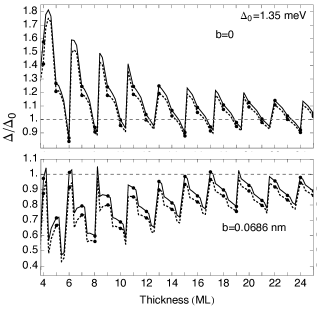
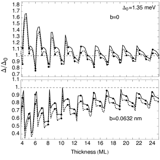
In this section, we consider the limit of no level broadening () with the substrate described by the asymmetric well (Fig. 1). The momentum-dependent order parameter is obtained from Eq. (3) where, as was mentioned in Sec. II.1, the superconducting gap is the minimum of the order parameter. We also approximate the solution of Eq. (3) by assuming a independent order parameter Eq. (4). In Figs. 3 and 4, we analyze the differences between the two predictions for different values of the asymmetric potential.
The pattern of shape resonances is
qualitatively similar in both cases. It is clear however that the approximate solution (4) is
always below the actual gap (3). This difference is more evident in Fig.
4 where the potential is shallower and the coupling to the substrate is therefore stronger. Given that the system of equations (3), can easily be
solved without any approximation, in principle there is no substantial advantage in using the
approximate solution. However, once a finite lifetime is considered, the approximate solution to the order parameter is still easily obtained from Eq.
(22), while the momentum-dependent order parameter ought to
be calculated from the integral equation (21),
is much more difficult to solve. For that reason, and because the results are qualitatively similar, we stick to Eq. (22) to compute the superconducting gap in the rest of the paper.
We are now ready to study the role of the substrate in our results.
In Fig. 3, we compute the superconducting gap with the parameters defined in Eq. (23).
For the film/substrate height we take eV which accounts for the
Fermi level mismatch with the substrate plus the height of the Schottky
barrier. In Fig. 4 we remove the Schottky barrier contribution leaving
eV where eV corresponds to the Fermi level mismatch with
the substrate. As was expected from the model used to couple the film to the
substrate, introduced in Sec. II.2.1, and the expressions of the BCS interaction
matrix elements, introduced in Sec. II.1, we observe that a
decrease of the potential height is accompanied by an average suppression of superconductivity. This is a simple consequence of two facts, the states are more extended into the substrate and the potential has
less bound states.
Moreover, as a consequence of the coupling to the substrate, the pattern of shape resonances differs from that of an infinite well Thompson and Blatt (1963) where decreases monotonically with the thickness until another state is occupied. Our results, depicted in Figs. 3 and 4, show as the potential height decreases, the momentum dependence of the order parameter becomes more relevant yielding an additional non monotonic behavior with additional features. These extra features are originated by the combined effect of the momentum-dependent interaction, the finite number of states in the asymmetric well, and the off-centered dispersion relation (5). The maxima and minima do not necessarily correspond to a different number of occupied states in the considered band ( band in Fig. 2).
As the thickness increases, the occupied states are lowered in the potential well (more bounded) which yields the moderate, smooth increase observed in the above plots between two prominent peaks. For some thickness the lower state in the upper band reaches the minimum at the point and thereupon this electron occupies a state in the lower band. At the same time another available state in the band is occupied and thus, even though the number of occupied states in the band is the same, these are higher in energy (less bounded) yielding a sudden decrease. Finally, for a larger thickness the number of occupied states in the band increases and a large increase is observed.
The previous figures show the effect of charge neutrality is qualitatively similar to that in an infinite potential well Yu et al. (1976), the average decreases the thinner the film is. Furthermore, as decreases, the charge neutrality correction, measured by , is smaller. In other words, both charge neutrality and a reduction of the potential height have a similar effect: to suppress superconductivity so that for all thicknesses the gap is below the bulk limit.
As was mentioned in Sec. II.2.2, the method used to impose charge neutrality is only valid in the limit . For Pb films in the range of thickness studied thickness, however, the validity of the method is less clear as the thickness decreases. Furthermore, it is still under discussion as to whether, or to what extent, this condition realizes in realistic nano-structures.Chaib et al. (2005)
III.2.2 Finite lifetime
We now study the role of a finite lifetime that describes tunneling out of the film and other sources of decoherence. Following results of previous sections we use the smoother density of states (11) to compute first the chemical potential (20) and finally the superconducting energy gap (22).
We assume a linear dependence of
with the thickness. Shape resonances in the
superconducting gap at zero temperature, depicted in Fig. 5, are
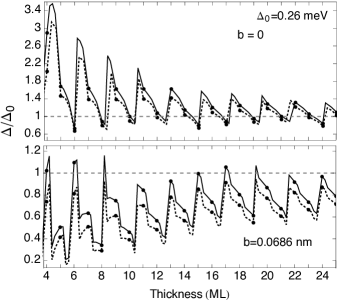
suppressed for comparable to [Eq. (27)], the time scale related to the mean level spacing in the asymmetric well potential. More
precisely, for Pb/Si films of less than ML the suppression is considerable
when (see the blue data). This suppression is clearer if one considers the experimentally accessible thicknesses (integer numbers of monolayers): the red and blue dots in the previous figure show that it is indeed expected to measure small oscillations in of a Pb thin film.
For smaller , the effect of level broadening completely smears size effects however in this range of lifetime the leading effect is to suppress superconductivity, , due to the modification introduced in the interaction matrix elements [Eq.(18)].
It is also clear that, especially for small thicknesses, charge neutrality is the dominant mechanism for suppression of superconductivity. It reduces substantially the value of the gap so that it is under the bulk value in the full range of parameters investigated.
III.2.3 Comparison with experiments
Recent STM experiments on a single monolayer of Pb deposited on Si Zhang et al. (2010) indicate sharp peaks in the tunneling data which correspond, approximately, to , two orders of magnitude larger than the one used here. This suggests that in this setting, tunneling into the substrate is negligible even for one atomic monolayer.
In this limit (see results depicted in Figs. 3 and 4), we have observed that, in agreement with the experimental results, size effects in the presence of the substrate, and including the charge neutrality condition, lead to a superconducting gap which is below the bulk limit. As the film thickness approaches the 1-ML limit, the exponential tails of the thin-film eigenstates into the substrate become longer and therefore we expect a strong suppression of the gap. Strictly speaking, this limit can not be studied quantitatively within our model since we neglect other effects that might become relevant in this situation, such as surface phonons or the enhancement of Coulomb interactions. However, our model still predicts a strong suppression superconductivity.
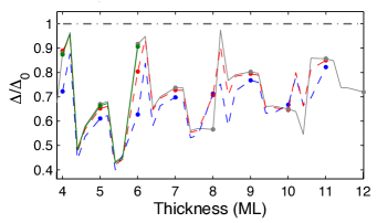
The results presented in Fig. 5, which include a finite lifetime, provide a good description of the superconducting gap in thin Pb/Si films obtained by transport measurements Guo et al. (2004). Our model reproduces correctly the small oscillations of the critical temperature observed experimentally in the region ML, the gradual suppression of the average gap as thickness is reduced and the smoothing of shape resonance for ML.
We note that the main difference between the two experiments is the presence of a capped layer in Ref. Guo et al. (2004) needed to carry out transport measurements. Even if tunneling into the substrate is negligible, as the STM results of Ref. Zhang et al. (2010) suggest, the film coupling to the overlayer still causes important decoherence effects which in our model correspond to a much smaller choice of than in the description of the STM experiment.
In summary, by tuning we are able to describe qualitatively the experimental results of Refs. Guo et al. (2004); Zhang et al. (2010). We note in the particular case of Pb/Si films the Si band gap in the crystallographic direction perpendicular to the interface yields a strong state confinement in the Pb film and thus tunneling into the substrate is suppressed. However, for other cases, such as Al films, the confinement is not caused Aballe et al. (2001b) by a band gap and thus tunneling can be a relevant source of decoherence that can be included with the model presented in Sec. II.2.3. Nonetheless, in this case it is likely that more sophisticated theoretical models of the interface are necessary for a quantitative description of the experimental results.
III.2.4 Weakly coupled superconductors
From the results of the previous section it seems rather unrealistic, at least in Pb, to enhance superconductivity by size effects. Lead is a strong coupled superconductor so it would be interesting to explore whether size effects are stronger in materials characterized by a weaker coupling constant . Indeed, from Eq. (4) it is straightforward to show that the first-order correction to is inversely proportional to the coupling constant . Therefore, the smaller , the larger the finite size correction. Even if charge neutrality applies, the oscillations of the superconducting gap are expected to show higher maxima, with respect to the bulk limit, for smaller which might lead to an enhancement of superconductivity. In this section, the dimensionless coupling constant is decreased to and the Debye energy is set to meV. We analyze the case of and maintain the same parameters for the band structure and the asymmetric potential [Eqs. (23)-(25)], as here our goal is to explore the dependence on the coupling constant rather than to model a specific material.
The results, depicted in Fig. 6, show a considerable enhancement of superconductivity when charge neutrality is not imposed. If it is included a moderate enhancement is still observed for a few values of the thickness. As for Pb, see Figs. 3 and 4, the exact solution (continuous line), Eq. (3), predicts a larger gap than the approximation, Eq. (4) (dashed line). Indeed we observe a net enhancement only in the case . This is a strong suggestion that an enhancement of superconductivity might occur for a finite lifetime provided that the gap is computed directly from Eq. (21). We note that the approximate solution (blue) shows no enhancement of with respect to the bulk limit even for so finite corrections, Eq. (22), would induce a further suppression of the energy gap.
In summary, weakly coupled superconducting materials are more promising candidates to observe an enhancement of superconductivity in thin films and nanostructures provided the quasiparticle lifetime is much larger than , Eq. (27).
IV Conclusions
We have investigated analytically the effect of the substrate on superconducting thin films. We aim to provide a description of recent Pb thin-film experiments and also to identify a region of parameters in which size effects could enhance superconductivity. Superconductivity is modeled by a mean-field formalism. The model of the coupling of the thin film to the substrate has three ingredients: an asymmetric quantum well, a finite quasiparticle lifetime (that describes tunneling into the substrate and other decoherence mechanisms), and the charge neutrality condition on the interfaces. For Pb on a Si substrate, we observe small oscillations, remnants of shape resonances, of the energy gap as thickness is decreased but always below the bulk limit for realistic values of the quasiparticle lifetime and the interface potential. This is fully consistent with the transport measurements of Ref. Guo et al. (2004) in which a capped layer induces additional level broadening, for sufficiently thin films. In the limit of negligible broadening our results are also consistent with the in situ STM experiments of Ref.Zhang et al. (2010) in which a capped layer is not present. For materials with a smaller electron-phonon coupling constant, size effects are stronger. We identify a range of parameters, fs, thicknesses ML, for which a modest enhancement of superconductivity is feasible even if charge neutrality holds. A stronger enhancement is expected provided that charge neutrality does not apply. This seems to be the case in complex oxide heterostructures.
Acknowledgements.
ARB acknowledges support from a la Caixa foundation fellowship. AMG acknowledges supports from EPSRC, grant No. EP/I004637/1, FCT, grant PTDC/FIS/111348/2009 and a Marie Curie International Reintegration Grant PIRG07-GA-2010-268172.References
- Thompson and Blatt (1963) C. J. Thompson and J. M. Blatt, Phys. Lett. 5, 6 (1963).
- Cohen and Abeles (1968) R. W. Cohen and B. Abeles, Phys. Rev. 168, 444 (1968).
- Kresin and Tavger (1966) V. Kresin and B. Tavger, Zh. Eksp. Teor. Fiz. 50, 1689 (1966), [Sov. Phys. JETP 23, 1124 (1966)].
- Allen (1975) R. E. Allen, Phys. Rev. B 12, 3650 (1975).
- Yu et al. (1976) M. Yu, M. Strongin, and A. Paskin, Phys. Rev. B 14, 996 (1976).
- Jaeger et al. (1989) H. M. Jaeger, D. B. Haviland, B. G. Orr, and A. M. Goldman, Phys. Rev. B 40, 182 (1989).
- Qin et al. (2009) S. Qin, J. Kim, Q. Niu, and C.-K. Shih, Science (New York, N.Y.) 324, 1314 (2009).
- Zhang et al. (2010) T. Zhang, P. Cheng, W.-J. Li, Y.-J. Sun, G. Wang, X.-G. Zhu, K. He, L. Wang, X. Ma, X. Chen, Y. Wang, Y. Liu, H.-Q. Lin, J.-F. Jia, and Q.-K. Xue, Nat. Phys. 6, 104 (2010).
- Brun et al. (2009) C. Brun, I. Hong, F. Patthey, I. Y. Sklyadneva, R. Heid, P. M. Echenique, K. P. Bohnen, E. V. Chulkov, and W.-D. Schneider, Phys. Rev. Lett. 102, 207002 (2009).
- Bose et al. (2010) S. Bose, A. M. García-garcía, M. M. Ugeda, J. D. Urbina, C. H. Michaelis, I. Brihuega, and K. Kern, Nat. Mat. 9, 550 (2010).
- Guo et al. (2004) Y. Guo, Y.-F. Zhang, X.-Y. Bao, T.-Z. Han, Z. Tang, L.-X. Zhang, W.-G. Zhu, E. G. Wang, Q. Niu, Z. Q. Qiu, J.-F. Jia, Z.-X. Zhao, and Q.-K. Xue, Science 306, 1915 (2004).
- Chen et al. (2006) B. Chen, Z. Zhu, and X. Xie, Phys. Rev. B 74, 132504 (2006).
- Shanenko et al. (2007) A. A. Shanenko, M. D. Croitoru, and F. M. Peeters, Phys. Rev. B 75, 014519 (2007).
- Jia et al. (2006) Y. Jia, B. Wu, H. H. Weitering, and Z. Zhang, Phys. Rev. B 74, 035433 (2006).
- Reyren et al. (2007) N. Reyren, S. Thiel, A. Caviglia, L. F. Kourkoutis, G. Hammerl, C. Richter, C. Schneider, T. Kopp, A.-S. Rüetschi, D. Jaccard, et al., Science 317, 1196 (2007).
- Liu et al. (2012) D. Liu, W. Zhang, D. Mou, J. He, Y.-B. Ou, Q.-Y. Wang, Z. Li, L. Wang, L. Zhao, S. He, Y. Peng, X. Liu, C. Chen, L. Yu, G. Liu, X. Dong, J. Zhang, C. Chen, Z. Xu, J. Hu, X. Chen, X. Ma, Q. Xue, and X. J. Zhou, Nat. Commun. 3, 931 (2012).
- Zubko et al. (2011) P. Zubko, S. Gariglio, M. Gabay, P. Ghosez, and J.-M. Triscone, Annu. Rev. Condens. Matter Phys. 2, 141 (2011).
- de Gennes (1964) P. G. de Gennes, Rev. Mod. Phys. 36, 225 (1964).
- Czoschke et al. (2005) P. Czoschke, H. Hong, L. Basile, and T.-C. Chiang, Phys. Rev. B 72, 075402 (2005).
- van Dijk and Nogami (2002) W. van Dijk and Y. Nogami, Phys. Rev. C 65, 024608 (2002).
- Kirchmann et al. (2010) P. S. Kirchmann, L. Rettig, X. Zubizarreta, V. M. Silkin, E. V. Chulkov, and U. Bovensiepen, Nat. Phys. 6, 782 (2010).
- Aballe et al. (2001a) L. Aballe, C. Rogero, P. Kratzer, S. Gokhale, and K. Horn, Phys. Rev. Lett. 87, 156801 (2001a).
- Horn et al. (1984) K. Horn, B. Reihl, A. Zartner, D. E. Eastman, K. Hermann, and J. Noffke, Phys. Rev. B 30, 1711 (1984).
- BenDaniel and Duke (1966) D. BenDaniel and C. Duke, Phys. Rev. 152, 683 (1966).
- Sugiyama (1960) A. Sugiyama, J. Phys. Soc. Jp. 15, 965 (1960).
- Garcia-Moliner and Flores (1979) F. Garcia-Moliner and F. Flores, Introduction to the Theory of Solid Surfaces (Cambridge University Press, 1979).
- Chan et al. (2003) T.-L. Chan, C. Z. Wang, M. C. Hupalo, M. Tringides, Z.-Y. Lu, and K. M. Ho, Phys. Rev. B 68, 045410 (2003).
- Brack and Bhaduri (1997) M. Brack and R. Bhaduri, Semicalssical Physics (Addison-Wesley, New York, 1997).
- Upton et al. (2004) M. H. Upton, C. M. Wei, M. Y. Chou, T. Miller, and T. C. Chiang, Phys. Rev. Lett. 93, 026802 (2004).
- Dil et al. (2006) J. Dil, J. W. Kim, T. Kampen, K. Horn, and A. Ettema, Phys. Rev. B 73, 161308 (2006).
- Anderson and Gold (1965) J. Anderson and A. Gold, Phys. Rev. 139, A1459 (1965).
- Pan et al. (2011) S. Pan, Q. Liu, F. Ming, K. Wang, and X. Xiao, J. Phys: Cond. Mat. 23, 485001 (2011).
- Dresselhaus et al. (1955) G. Dresselhaus, A. Kip, and C. Kittel, Phys. Rev. 98, 368 (1955).
- Heslinga et al. (1990) D. R. Heslinga, H. H. Weitering, D. P. vanderWerf, T. M. Klapwijk, and T. Hibma, Phys. Rev. Lett. 64, 1589 (1990).
- Eom et al. (2006) D. Eom, S. Qin, M. Y. Chou, and C. K. Shih, Phys. Rev. Lett. 96, 027005 (2006).
- Poole et al. (2007) C. J. Poole, H. Farach, and R. Creswick, Superconductivity, 2nd ed. (Academic Press, Amsterdam, 2007).
- Chaib et al. (2005) H. Chaib, L. Eng, and T. Otto, J. Phys: Cond. Mat. 17, 161 (2005).
- Aballe et al. (2001b) L. Aballe, C. Rogero, S. Gokhale, S. Kulkarni, and K. Horn, Surf. Sci. 485, 488 (2001b).