A first principles investigated optical spectra of oxizided graphene
Abstract
The electronic and optical properties of mono, di, tri, and tetravacancies in graphene are studied in comparison to each other, using density functional theory. In addition, oxidized monovacancies are considered for different oxygen concentrations. Pristine graphene is found to be more absorptive than any defect configuration at low energy. We demonstrate characteristic differences in the optical spectra of the various defects for energies up to 3 eV. This makes it possible to quantify by optical spectroscopy the ratios of the defect species present in a sample.
While graphene is a zero band gap material, but a finite band gap is needed for various applications aiming at graphene based electronic devices schwierz ; kaloni3 . Functionalization is one of the possible methods to open a band gap for example by simple oxidation wu ; priya ; kaloni . Graphene oxide (GO) with epoxy, carbonyl, or hydroxyl groups could allow to tune the a band gap and therefor tailor the electronic, mechanical, and optical properties dai ; andre . The atomic structure of GO has been studied experimentally weiwei ; ajayan and theoretically sumit . Recently, GO nanostructures have created a lot of attention due to the fact that it paved the way for solution based synthesis of graphene sheets, low cost, easy processibility, and compatibility with various substrates Joung . The band gap of GO can be tunable by just varying the oxidation level. Fully oxidized GO can act as an electrical insulator and partially oxidized GO can act as a semiconductor Loh . Moreover, experiments demonstrat that GO nanostructures have promising applications in photocatalysis Krishnamoorthy . Reduction of GO may pave the way to mass production of graphene shenoy .
While GO is usually insulating, a controlled deoxidation can lead to an electrically and optically active material that is transparent and conducting. Furthermore, in contrast to pristine graphene, GO is fluorescent over a broad range of wavelengths, owing to its heterogeneous electronic structure Loh . It can contain different chemical compositions of carbon, oxygen, and hydrogen weiwei ; lu . While commonly hydroxyl and epoxy groups are found, there can be small contributions of carbonyl and carboxyl groups. Experimentally, a coverage of between 25% and 75% has been observed, reflecting that typically a quarter of the CC bonds are double bonds whereas the rest are single bonds Katsnelson . Adsorption behavior of oxygen atoms on the graphene sheets has been studied by using first-principles calculations ito and found that the lattice constant increases with the increase of the ratio of because of the formation of the epoxy group. At 50% ratio, a finite band gap of 3.39 eV is reported ito .
The attachment of a carbonyl group leads to an almost planar electronic configuration because the formation of C=O bonds induces little strain in the graphene sheet. On the contrary, the attachment of an epoxy group leads to a non-planar distorted electronic configuration for those C atoms which are connected to O, which creates a significant strain on neighboring CC bonds shenoy . The combination of and configurations as well as defects breaks the hexagonal symmetry of pristine graphene and a band gap is opened. The coexistence of and configurations is confirmed experimentally yun and theoretically shenoy . The defects associated with dangling bonds enhance the reactivity substantially.
Recently, a theoretical investigation of the electronic and optical properties of GO (without vacancies) for different functional groups and various compositions has been reported in Ref priya . The authors found that carbonyl groups are favourable for photoluminescense and that the optical gap of reduced GO is samaller than the optical gap of pristine and fully oxidize graphene. Theoretical and experimental studies Katsnelson1 ; Wang indicate that hydroxyl, carboxyl, and other functional groups can easily be attached to vacancies in graphene than to pristine graphene. Therefore, a study of the electronic and optical properties of defective GO becomes critical. Optical properties of oxidized mono-, di-, tri-, and tetra-vacancies in graphene have not been reported so far. In this work, we use first principles calculations of to provide insight into this topic.
Our calculations are based on density functional theory and carried out using the generalized gradient approximation of Quantum Espresso pacakage, paolo ; pbe . All calculations are performed with a plane wave cutoff energy of 544 eV. We use a Monkhorst-Pack Monk of k-mesh for the Brillouin zone integration in order to relaxing the structures and achieving highly accurate electronic structure. We observe that a supercell of graphene is sufficiently large for monovacancies and oxidized monovacancies kaloni . Our supercell has a lattice constant of Å and extends Å in the perpendicular direction. It has been reported that nearby vacancies behave independently when they are separated by 7 Å andrey . Hence, we use a supercell for di-, tri-, and tetra-vacancies to avoid artificial interaction of the periodic images. This supercell has a lattice constant of Å and again Å. The cell parameters and atomic positions are fully relaxed until a force convergence of 0.05 eV/Å and an energy convergence of 10-7 eV are reached. The relaxed structures are used to calculate the optical properties by WIEN2k Wien2k code. For the optical calculations, a dense mesh of uniformely distributed k-points is required. Hence, the Brillouin zone integration is performed using tetrahedron method with 180 k-points in the irreducible part of the Brillouin zone. Well converged solutions are obtained for =7, where is the plane-wave cut-off and is the smallest of all atomic sphere radii.
The dielectric function () is known to describe the optical response of the medium. The interband contribution to the imaginary part of the dielectric function is calculated by summing all transitions from occupied to unoccupied states (with fixed k) over the Brillouin zone, weighted with the appropriate matrix elements giving the probability for the transitions. The imaginary part of dielectric function is given as in wooten by
| (1) |
Where M is dipole matrix, i and j are the initial and final states, respectively, is the Fermi distribution function for the states, and is the energy of electron in the state. The real part of the dielectric function can be extrated from the imaginary part using the Kramers-Kronig relation wooten ; Yu in the from
| (2) |
Where P implies the principle value of the integral.
The reflectivity spectra are derived from Fresnel’s formula for normal incidence assuming an orientation of the crystal surface parallel to the optical axis using the relation fox
| (3) |
The knowledge of both real and imaginary parts of the dielectric tensor allows the calculations of the important optical functions. We calculate the absorption, the real part of optical conductivity, and the electron energy-loss spectrum using the following expressions fox ; delin
| (4) |
| (5) |
| (6) |
This approach has been successfully applied to narrow band gap materials including rare earth Zintl compounds Zintl ; Zintl1 , and oxides singh . For a reliable integration, a set of 180 k-points in the irreducible wedge of the Brillouin zone is used. A Lorentzian broadening is used to simulate the effects of finite life-time and finite resolution of the optical measurement.
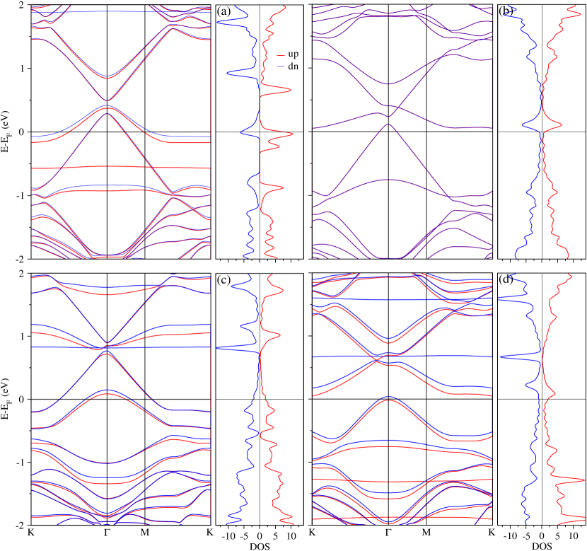
The calculated values of formation energy of mono-, di-, tri-, and tetra-vacancies in graphene are 7.50, 6.94 eV, 11.45 eV, and 12.58 eV, respectively. This means the formation of a divacancy in graphene is more favourable than the formation of a single vacancy. Furthermore, a divacancy is known to be more stable than two isolated monovacancies (whose migration energy barrier is rather low), because the dangling C-C bonds of atoms next to the vacancy can be passivated by eachother Lee . The vacancies in graphene induce ferromagnetism with total magnetic moments of 1.35 , 1.00 , 2.00 for mono-, tri-, tetra-vacancies, respectively. Di-vacancies shows no spin-polarization. The results of our band structure (BS) calculations for mono-, di-, tri-, and tetra-vacancies are shown in Fig. 1 together with the corresponding DOS. For the sake of comparison we have included the BS (dotted lines) of pristine graphene. For an oxidized monovacancy, the magnetic and electronic properties have been reported in previous literature kaloni ; dai ; Yazyev . In supercell, the Dirac cone is shifted to the -point due to Brillouin zone folding in supercell. In case of the tetra-vacancy, the BS shows that a single minority spin band crosses the Fermi energy () at the -point and leaves the system metallic, whereas for the di-, tri-vacancies both majority and minority bands cross . Moreover, an upward shift of the Dirac point is indicative of a hole-doped system. In case of the di-vacancy, the DOS is identical for the majority and minority spins, reflecting spin-degeneracy. It means pristine graphene becomes ferromagnetic by a single vacancy defect and can be non-magnetic metal by divacancy.
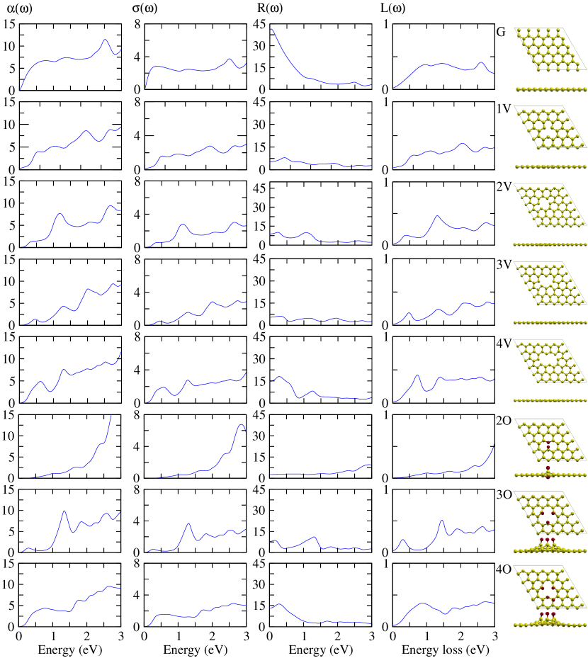
The optical spectroscopy is a valuable tool in material science. Here, In the optical calculations, selfenergy and excitonic effects are not taken into account. It has been shown for graphene that in the energy range upto 3 eV, where the approximation of Dirac particles is valid, the influence of the many-particle effects is negligible. The calculated optical spectra of pristine graphene and its functionalized derivatives are addressed in Fig 1. The optical spectra show that for the two adsorbed O atoms, a band gap of 0.5 eV is opened due to the symmtery breaking and increased characters. A semiconducting behaviour for this configuration is conformed by our previous calculations of BS and DOS kaloni . As comparised to pristine graphene, all defects are found to create metallic states as shown in Fig 1.
In general, pristine graphene is more absorptive as compared to the other systems but for di-vacancy, absoption between 7.5 eV to 10 eV is higher than pristine graphene. The peak at 4.5 eV for pristine graphene splits into two peaks at 2.7 eV and 5 eV by the splitting of the Dirac cone for two attached O atoms. The splitting increasing with the O coverage. For di-vacancy and three adsorbed O atoms an additional sharp peak at 1.25 eV (visible region) is found which is absent for other systems. The pristine graphene have high reflectivity in the low energy as compared to other cases. The reflectivity is higher for the tetra-vacancy (most pronounced metallicity) as compare to mono-, di-, and tri-vacancies, but lower than for pristine graphene. The reflectivity in low energy range is the lowest for the case of monovacancy with two attached O atoms, due to its semiconducting nature and increases again for three and four attached O atoms. The most prominent peaks in become broaden and the magnitude also decreases as one moves from pristine graphene to tetra-vacancies. The is low for tri-, tetra-vacancies and monovacancy with four attached O atoms as compared to remaining systems. A large peak is observed at around 4.6 eV in all optical spectra for all the systems which is attributed to the transitions of the aromatic CC atoms. The maximum peak in energy loss spectra is at 4.9 eV, which is assigned to the energy of the volume plasmon . This maximum peak positions remain same for all systems. The peaks in optical spectra originates from the transition from valence band to conduction band. The dominating peak in the energy loss spectrum broadens from graphene to the oxidize vacancies with monovacancy.
In conclusion, we have studied the optical properties of graphene derivatives (clean and oxidized vacancies) by means of density functional theory. We find that the formation of divacancies in graphene is energetically favourable. Divacancies are also exceptional in the sense that they do not lead to a local magnetic moment. Mono, di, tri, and tetravacancies are found to be metallic, while an oxidized monovacancy with two adsorbed oxygen atoms leads to a band gap of 0.5 eV (due to a splitting of the Dirac cone). Our optical spectra show that pristine graphene has the highest absorption in the energy range below 2.5 eV. In two cases (tetravacancy and monovacancy with three adsorbed oxygen atoms) a prominent absorption peak appears in the visible range. Our calculations suggest that the types of (oxidized) defects present in a graphene sample can be quantified by optical spectroscopy. With this knowledge, the electronic and optical properties of graphene derivatives can be tuned by controlled oxidation and reduction.
References
- (1) F. Schwierz, Nat. Nanotechnol. 5, 487 (2010).
- (2) T. P. Kaloni, Y. C. Cheng and U. Schwingenschlögl, J. Mater. Chem. 22, 919 (2012)
- (3) X. Wu, M. Sprinkle, X. Li, F. Ming, C. Berger, and W. A. de Heer, Phys. Rev. Lett. 101, 026801 (2008)
- (4) P. Johari and V. B. Shenoy, ACS Nano 9, 7640 (2011).
- (5) T. P. Kaloni, Y. C. Cheng, R. Faccio, and U. Schwingenschlögl, J. Mater. Chem. 21, 18284 (2011).
- (6) J. Dai and J. Yuan, Phys. Rev. B 81, 165414 (2010).
- (7) K. A. Mkhoyan, A. W. Contryman, J. Silcox, D. A. Stewart, G. Eda, C. Mattevi, S. Miller, and M. Chhowalla, Nano Lett. 9 1058 (2009).
- (8) W. Cai, R. D. Piner, F. J. Stadermann, S. Park, M. A. Shaibat, Y. Ishii, D. Yang, A. Velamakanni, S. J. An, M. Stoller, J. An, D. Chen, and R. S. Ruoff, Science 321, 1815 (2008).
- (9) W. Gao, L. B. Alemany, L. Ci, and P. M. Ajayan, Nat. Chem. 1, 403 (2009).
- (10) S. Saxena, T. A. Tyson, S. Shukla, E. Negusse, H. Chen, and J. Bai, Appl. Phys. Lett. 99, 013104 (2011).
- (11) D. Joung, A. Chunder, L. Zhai, and S. I. Khondaker, Appl. Phys. Lett. 97, 093105 (2010)
- (12) K. P. Loh, Q. Bao, G. Eda, and M. Chhowalla, Nat. Chem. 2, 907 (2010).
- (13) K. Krishnamoorthy, R. Mohan, and S. J. Kim, Appl. Phys. Lett. 98, 244101 (2011).
- (14) A. Bagri, C. Mattevi, M. Acik, Y. J. Chabal, M. Chhowalla, and V. B. Shenoy, Nat. Chem. 2, 581 (2010).
- (15) N. Lu, Y. Huang, H.-B. Li, Z. Li, and J. Yang, J. Chem. Phys. 133, 034502 (2010).
- (16) D. W. Boukhvalov and M. I. Katsnelson, J. Am. Chem. Soc. 130, 10697 (2008).
- (17) J. Ito, J. Nakamuraa, and A. Natori, J. Appl. Phys. 103, 113712 (2008).
- (18) H. K. Jeong, Y. P. Lee, R. J. W. E. Lahaye, M.-H. Park, K. H. An, I. J. Kim, C.-W. Yang, C. Y. Park, R. S. Ruoff, and Y. H. Lee, J. Am. Chem. Soc. 130, 1362 (2008).
- (19) D. W. Boukhvalov and M. I. Katsnelson, Nano Lett. 8, 4373 (2008).
- (20) X. Wang, S. M. Tabakman, and H. Dai, J. Am. Chem. Soc. 130, 8152 (2008).
- (21) P. Giannozzi, S. Baroni, N. Bonini, M. Calandra, R. Car, C. Cavazzoni, D. Ceresoli, G. L. Chiarotti, M. Cococcioni, I. Dabo, A. Dal Corso, S. de Gironcoli, S. Fabris, G. Fratesi, R. Gebauer, U. Gerstmann, C. Gougoussis, A. Kokalj, M. Lazzeri, L. Martin-Samos, N. Marzari, F. Mauri, R. Mazzarello, S. Paolini, A. Pasquarello, L. Paulatto, C. Sbraccia, S. Scandolo, G. Sclauzero, A. P. Seitsonen, A. Smogunov, P. Umari, and R. M. Wentzcovitch, J. Phys. Condens. Matt. 21, 395502 (2009).
- (22) J. P. Perdew, K. Burke, and M. Ernzerhof, Phys. Rev. Lett. 77, 3865 (1996).
- (23) H. J. Monkhorst and J. D. Pack, Phys. Rev. B 13, 5188 (1976).
- (24) V. V. Nelayev and A. I. Mironchik, Materials Phys. and Mechanics 9, 26 (2010).
- (25) P. Blaha, K. Schwarz, G. Madsen, D. Kvasicka, and J. Luitz, WIEN2k, An Augmented Plane Wave + Local Orbitals Program for Calculating Crystal Properties (Technical University of Vienna, Vienna, 2001).
- (26) F. Wooten: Optical Properties of Solids (Academic Press, New York, 1972).
- (27) Y. P. Yu and M. Cardona 1999 Fundamentals of Semiconductors: Physics and Materials Properties 2nd edn, Berlin: Springer (1999)
- (28) M. Fox, Optical Properties of Solids, New York: Oxford University Press (2001).
- (29) A. Delin, O. Eriksson, R. Ahuja, B. Johansson, M. S. S. Brooks, T. Gasche, S. Auluck and J. M. Wills, Phys. Rev. B 54 1673 (1996).
- (30) N. Singh and U. Schwingenschlögl, Chem. Phys. Lett. 508, 29 (2011).
- (31) N. Singh and U. Schwingenschlögl, Appl. Phys. Lett. 100, 151906 (2012).
- (32) D. J. Singh, R.C. Rai, J.L. Musfeldt, S. Auluck, N. Singh, P. Khalifah, S. McClure, and D. G. Mandrus, Chem. Mat. 18, 2696 (2006).
- (33) G.-D. Lee, C. Z. Wang, E. Yoon, N.-M. Hwang, D.-Y. Kim, and K. M. Ho, Phys. Rev. Lett. 95, 205501 (2005).
- (34) O. V. Yazyev and L. Helm, Phys. Rev. B 75, 125408 (2007).