AuthorComment \defineavatarGHauthor=Gregor Hlawacek,color=yellow,opacity=0.5,voffset=5pt \pdfcommentsetupavatar=GH
Helium Ion Microscopy
Abstract
Helium Ion Microcopy (HIM) based on Gas Field Ion Sources (GFIS) represents a new ultra high resolution microscopy and nano–fabrication technique. It is an enabling technology that not only provides imagery of conducting as well as uncoated insulating nano–structures but also allows to create these features. The latter can be achieved using resists or material removal due to sputtering. The close to free–form sculpting of structures over several length scales has been made possible by the extension of the method to other gases such as Neon. A brief introduction of the underlying physics as well as a broad review of the applicability of the method is presented in this review.
I Introduction
High resolution imaging, in particular in biology and materials science, is mostly done using Scanning Electron Microscopy (SEM). The ease of use and the widespread availability has made this the number one method for imaging in the aforementioned fields. Structuring and manipulation of nano–sized features is traditionally the domain of Focused Ion Beams. Here, mainly liquid metal ion sources (LMIS) using Gallium are used. However, other techniques such as various types of GFIS,Tondare (2005) alloy LMIS,Bischoff (2005) magneto optical trap sources (MOTIS)Hanssen et al. (2008) and multicusp plasma sourcesJi et al. (2002) are runners–up. Good reviews discussing these two techniques can be found in Refs. [Goldstein et al., 2003] and [Utke, Hoffmann, and Melngailis, 2008] for SEM and FIB, respectively.
Helium Ion Microscopy presents a technique that unites many of the advantages of SEM and FIB in a single tool. More importantly, it also overcomes some of the deficiencies of SEM and FIB. In particular, the possibility to image biological and in general insulating samples without coating at highest resolution is important for many scientific questions currently discussed in materials science and biology. Another important charged particle beam technique—namely Transmission Electron Microscopy (TEM)—depends on very thin samples free of defects from the preparation. The unique nano–sized beam of the HIM makes it possible to not only mill and pattern smallest features but also do this with minimal damage to the crystal lattice.
In the following we will give an outline of the working principle and signal generation in helium ion microscopy, followed by two sections highlighting specific imaging applications and examples of materials modification.
I.1 Working principle
The initial idea of a scanning ion microscope has been put forward by Knoll and Ruska already in 1932.Knoll and Ruska (1932) The working principle of a helium ion microscope can be divided into three different stages.
-
1.
Helium ionization and acceleration
-
2.
Beam formation and control
-
3.
Sample interaction
In this introduction we will only briefly touch points 1 and 2. Instead, we will focus on the physics that is important to understand the application of the technique to imaging and nanofabrication.
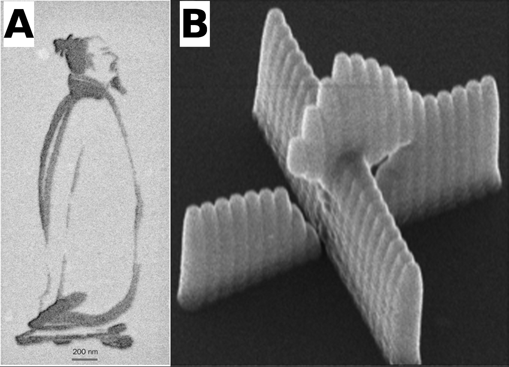
The first is made possible by using a newly developed Gas Field Ion Source (GFIS). GFIS have been investigated for a long timeOrloff and Swanson (1979); Tondare (2005); Horiuchi, Itakura, and Ishikawa (1988a); Sato (1992) for their use in microscopes.Escovitz, Fox, and Levi-Setti (1975); Orloff and Swanson (1975); Itakura, Horiuchi, and Yamamoto (1985); Horiuchi, Itakura, and Ishikawa (1988b) The idea is based on the initial design of a field ion microscope by E. Müller.Müller (1951); Melmed (1996) However, only recently a stable ion source with a high brightness and small virtual source size has been realized by Ward, Notte and Economou for use in a microscope.Ward, Notte, and Economou (2006) It is based on an emitter whose apex has been shaped into a three sided pyramid (see Fig. 1). Work is done currently to understand and optimize the supertip formation process in order to maximise the achievable current.Kalbitzer (2004); Pitters et al. (2013); Urban, Wolkow, and Pitters (2012); Urban, Pitters, and Wolkow (2012); Pitters, Urban, and Wolkow (2012); Rahman et al. (2013)
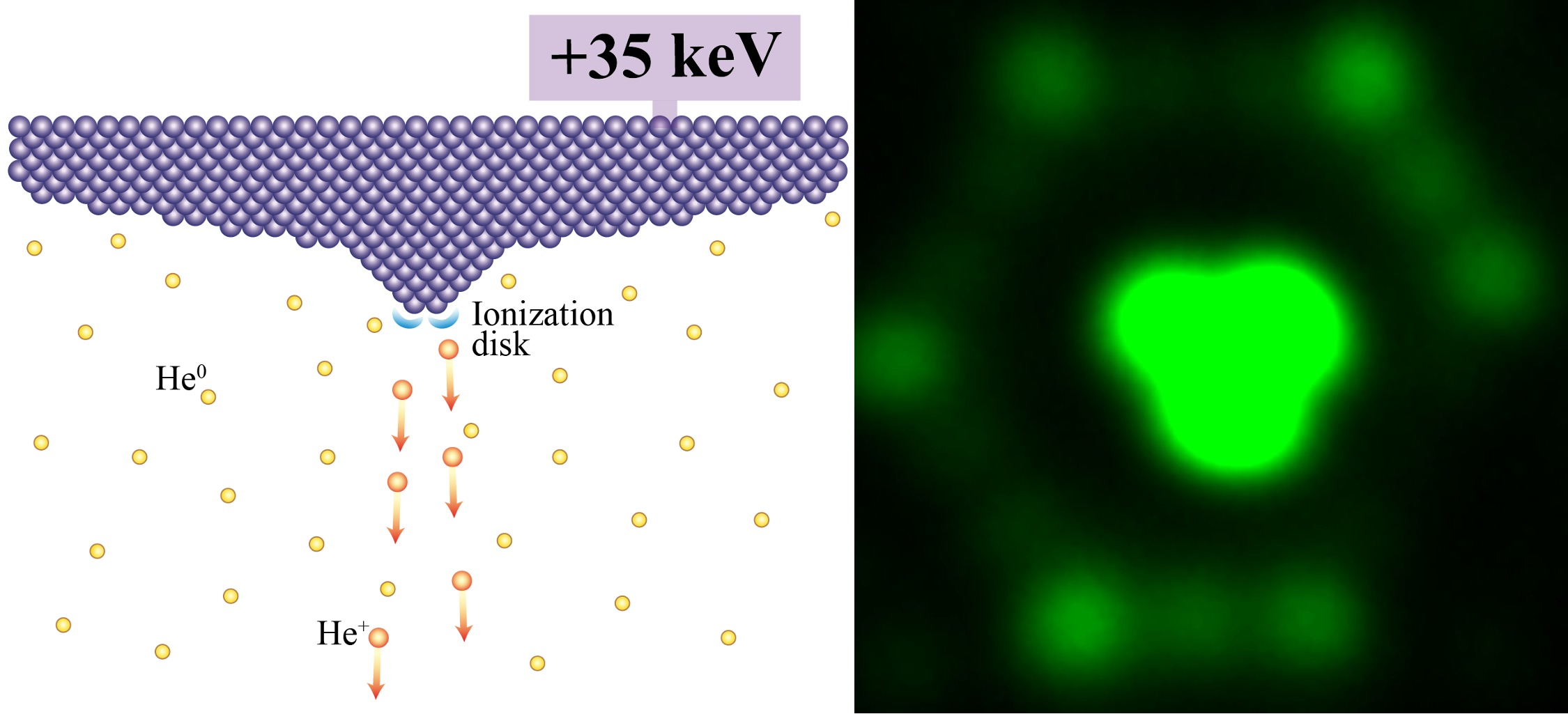
Using Scanning Field Ion Microscopy (SFIM) the apex of the tip can be monitored and shaped using high fields that can ultimately remove weakly bound atoms from the apex. In this way the configuration of the tip apex can be controlled at the atomic level. Although monomers are possible, trimers are more stable. Figure 1(b) shows a SFIM image of the tip. The trimer in the center and the edge of the first two shelves below the trimer are visible. The combination of a pyramidally shaped tip and the carefully shaped apex concentrates the electric field, so that subsequent helium ionization predominantly happens at the top most atoms of the pyramid. Using apertures in the beam path allows to select current originating from ionization events on a single apex atom. Typical source parameters are listed in table 1.
| Virtual source size | 0.25 nm | estimated |
| Angular intensity | 0.5–1 µA sr-1 | measured |
| Brightness | A cm-2sr-1 | calculated |
| Energy spread | 1 eV (0.25 eV – 0.5 eV)Ernst et al. (1993) | measured |
The second point is technologically demanding and requires a high degree of knowledge on the design and implementation of the involved electrostatic lenses, quadrupoles, octopoles, etc. For more details the reader is refereed to numerous monographs available on charged particle optics such as [Orloff, Utlaut, and Swanson, 2003; Rose, 2009]. The critical source parameters important for the ion optical performance of the column are given in table 1. The energy spread of 1 eV is an upper bound. Earlier measurements indicate that the values could in fact be lower by a factor of two to four.Ernst et al. (1993) One of the important consequences of the parameters listed in table 1 is the image side beam convergence angle . Typical values for are well below 1 mrad. This small beam divergence results in a large depth of field
| (1) |
Here, denotes the minimum feature that can be resolved in the image. Assuming identical resolutions the HIM will have a superior depth of field as compared to low–voltage SEM with typical values of 8 mrad.Hill, Notte, and Ward (2008)
Once the focused ion beam strikes the sample, the interaction of the accelerated particles with the substrate atoms and electrons will give rise to a large number of different signals. We will cover the available signals in the following section. Before we do so, we will briefly discuss the processes that occur during ion/sample interaction and that are important for the achievable resolution in charged particle beam imaging. Besides the small beam diameter, the shape and size of the actual interaction volume between the impinging particle and the sample plays an important role to reach ultimate resolution.
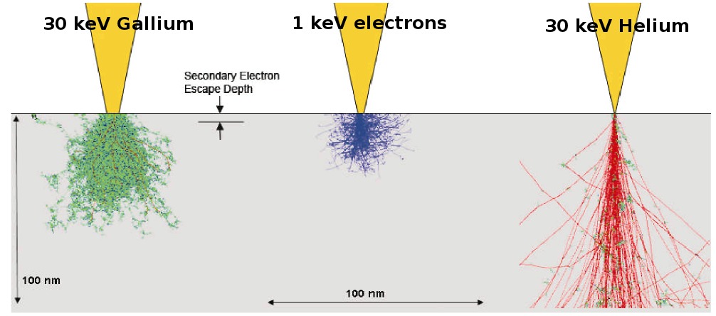
Figure 2 compares Monte Carlo (MC) simulation results for different charged particle beams. From the figure it is evident that the interaction volume relevant for secondary electron (SE) generation of the focused He beam is smaller than for the other two.Notte et al. (2007) For the case of a Ga beam the large cross section of Ga with—in this case Si—leads to substantial scattering in the near surface region relevant for the SE signal generation. For a low energy electron beam—needed to simultaneously optimize resolution and surface sensitivity in SEM—electron–electron scattering in the sample widens the beam dramatically in the first few nanometers deteriorating the achievable resolution. Scattering also occurs in HIM. In the case of a 30 keV He beam scattering occurs with the nuclei of the sample atoms. However, due to the low mass of helium, scattering is not very efficient in the first few nanometers of sample material. This results in minimal beam divergence inside the sample. Consequently the collected SE originate from a cylinder with a minimal volume. The somewhat lower energy of the SE in HIMPetrov and Vyvenko (2011) and the lower characteristic escape depth for SE in HIM for light elementsRamachandra, Griffin, and Joy (2009) enhances this difference between SEM and HIM even further.
I.2 Signals
Next we will discuss available particles and correoponding signals. We will in particular highlight their benefits and drawbacks when used for imaging and what kind of physical quantities can be accessed using them. The sequence in which they are discussed is determined by their abundance in the tool. This also corresponds to the ease of use and how widespread the technique is available in the current instrument base. An initial overview of some of the different contrast mechanisms is given by Bell.Bell (2009); Scipioni et al. (2009)
I.2.1 Secondary electrons
Secondary electron (SE) emission generated by ions can be split into two parts. In the logical order we will first discuss SE generation followed by the transport of electrons through the material. The latter is important as the generated electrons still need to reach and subsequently leave the surface into the vacuum so they can be detected. As has been proposed by BetheBethe (1941) the rate of secondary electron generation (electrons per incoming ion) is proportional to the stopping power of the incident particle in eV/Å.
| (2) |
Here, denotes a scaling constant. It is assumed that at least in the relevant near surface region, atomic collisions do not play an important role and depends only on the electronic stopping power.
The generated SE1 are mostly excited by the incoming ions via kinetic emission (KE).Ohya et al. (2008) Two types of secondary electrons of type 2 (SE2) exist in ion beam imaging. Type 2 electrons can be generated either by recoiling target atoms or from other SEs of type 1. The second type of SE2 generation (SE generated by SE) does not play an important role in HIM. This becomes clear when looking at the maximum energy of the SE, which is taken to be equal to the energy loss of the impinging He for a head–on collisionOhya et al. (2008); Rösler (1985)
| (3) |
Here, is the electron mass, the ion velocity, and denotes the Fermi–velocity. The cross section for such a collision is highest if the ion velocity— m/s for a primary energy of 35 keV—matches the Fermi–velocity of the electrons in the material. For gold and 35 keV He this yields a maximum SE energy of 45 eV. However, this energy is approximately equal to—or even below—the effective energy needed for SE generation by electrons in many materials.Lin and Joy (2005) Thus the size of the electron–electron collision cascade is restricted.
However, kinetic excitation of electrons is also possible by recoil atoms, provided they are fast enough so that their speed still matches the Fermi–velocity of the target material. Electrons produced by recoiling target atoms are usually called SE2. Ramachandra et al.Ramachandra, Griffin, and Joy (2009) calculated the ratio between SE2 and SE1 as function of energy and material. The conclusion that can be drawn from their calculation is that for higher primary energies a smaller SE2/SE1 ratio can be achieved for most materials and consequently a higher resolution is possible.
The other process for electron emission is potential emission (PE) via Auger neutralization. However, only for very low energies below 5 keV PE becomes dominantFerrón et al. (1981); Ramachandra, Griffin, and Joy (2009) over KE.
Once secondary electrons have been generated they still need to escape from the solid. This process can be described as a diffusion process. The characteristic length scale of this diffusion process—the effective diffusion length of secondary electrons —is of the order of 1 nm for nearly all materials.Ramachandra, Griffin, and Joy (2009) This leads to the fact that only the first few nanometers of the material add to the emitted SEs. Measurements of the effective SE yield in HIM show variations between 1 for carbon and values as high as 8 for platinum.Notte et al. (2007)
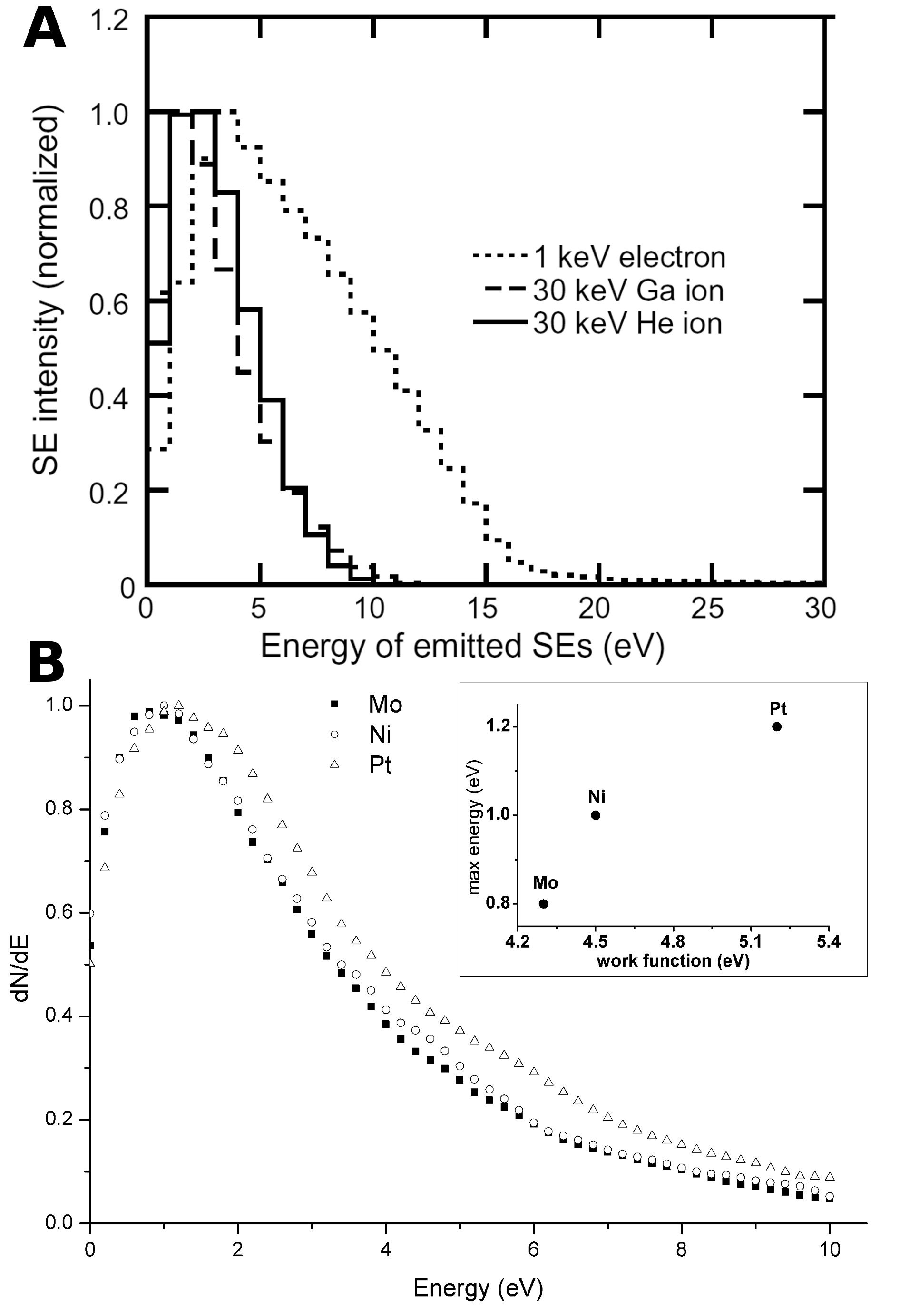
The number and energy distribution of these ion induced secondary electrons differs from what is found in a SEM. A sharper maximum at lower energies is usually foundOhya et al. (2009); Petrov, Vyvenko, and Bondarenko (2010) in HIM. In Fig. 3(a) a comparison of calculated SE yields in SEM, Ga–FIB and HIM is presented. The calculations done by Ohya et al. still overestimate peak position as well as peak width.Petrov and Vyvenko (2011) These differences between actual measurement results of SE yields in a HIM and calculations are attributed to SE generation mechanisms not considered in the calculations. Indications exist that bulk plasmon excitations can play an important rolePetrov and Vyvenko (2011); Riccardi et al. (2000) for SE generation in HIM. An actual measurement of SE yield as a function of SE energy and the work function dependence of the distribution maximum is presented in Fig. 3(b).
A consequence of the particular energy distribution of SE in HIM and the small SE generation volume is an enhanced surface sensitivity. This has been shown in a recent comparative study of HIM and SEM imaging performance on carbon coated gold nano–rods.Hlawacek et al. (2013) Only at very low acceleration voltages is SEM able to visualize the thin carbon layer covering the gold particles. However, low voltage SEM suffers from carbon deposition in the imaged area making detailed studies challenging. An example of the high sensitivity of HIM with respect to the material work function is the visualization of different half unit cell surface termination in Ti3SiC2.Buchholt et al. (2011) Depending on the position of the cleavage plane the surface is either terminated by Si (half unit cell) or Ti (full unit cell). The difference in the chemistry of the top surface layer of atoms results in different SE yields for the two terminations. As a result they can be discriminated in HIM.
A software package called IONiSE developed by P. Rack and coworkers is available that allows the calculation of the expected SE yield for a large number of materials.Ramachandra, Griffin, and Joy (2009) Although good agreement has been achieved between simulation and experiment, only a limited number of analytical applications based on SE yield are known.Petrov and Vyvenko (2011)
Sample topography in HIM is made visible in a similar way as in SEM. The dependence of the SE yield on the specimen tilt with respect to the incoming beam can be described the following secant law
| (4) |
However, experimental studies showed that the actually measured SE yield at the detector deviates from the expected secant behaviour.Bell (2009) The deviations lead to a more linear response curve, which in turn should reduce the strong edge effect known from SEM. Nevertheless, a very strong edge effect has been observed in thin layers.Behan et al. (2012); Fox et al. (2013)
In summary, the achievable high resolution and surface sensitivity in HIM is based on the fact that the SEs originate from a cylinder at the beam penetration point with a diameter of approximately 1 nm—given by the beam diameter—and a length of less than 3 nm—determined by . This small probe volume helps to achieve very high image resolution in HIM. It should be noted that obtaining such high resolution images has become substantially easier since the introduction of UHV HIM.van Gastel et al. (2011) At small fields of views usually high fluences are reached as a consequence of the large pixel density. In an UHV HIM implantation and sputtering can still negatively affect the sample during imaging. Carbon deposition on the other hand can be excluded.Veligura et al. (2012) The removal of hydrocarbons from the sample chamber vacuum prevents the formation of carbon deposits in the imaged area. As a consequence some exceptional imaging results could be achieved (see Fig. 6(b)).
I.2.2 Backscattered helium
What backscattered electrons are to the SEM, backscattered helium (BSHe) atoms and ions are to HIM. This rather bold statement is true in several ways, as will be highlighted in the next paragraphs.
Two different ways to utilize BSHe are available in current HIM. First, and most commonly used, is a microchannel plate (MCP) detector to acquire qualitative element distribution maps. Second, a silicon drift detector can be used to obtain spectroscopic information from microscopic areas. The latter allows quantitative element identification based on the same principles as Rutherford backscattering spectroscopy (RBS).
While SE images usually are rich in morphological contrast, BSHe images obtained with the MCP are poor in topography and rich in elemental contrast. In contrast to the SE images, the information in these images originates from the bulk of the sample. To measure them the MCP is inserted below the pole piece in the primary beam path. While a center hole allows the primary beam to reach the sample, this geometry maximizes the solid angle, and thus the collection efficiency of the detector. The obtained contrast can be understood by examining the Rutherford scattering cross section
| (5) |
where is the elementary charge, and and denote the atomic number of impinging and target particle, respectively. Assuming that the target atom is at rest, is the energy of the impinging particle, is an arbitrary element of solid angle, and is the scattering angle. For fixed —helium for this review—and a given energy, a dependence on leads to a strong contrast between different elements. A more detailed analysis of the scattering cross section shows that a dependence that is related to the structure of the periodic table of elements also exists. This is a result of the change in screening along the rows of the periodic table. In Fig. 4, experimentally obtained BSHe yields for various elements are presented.
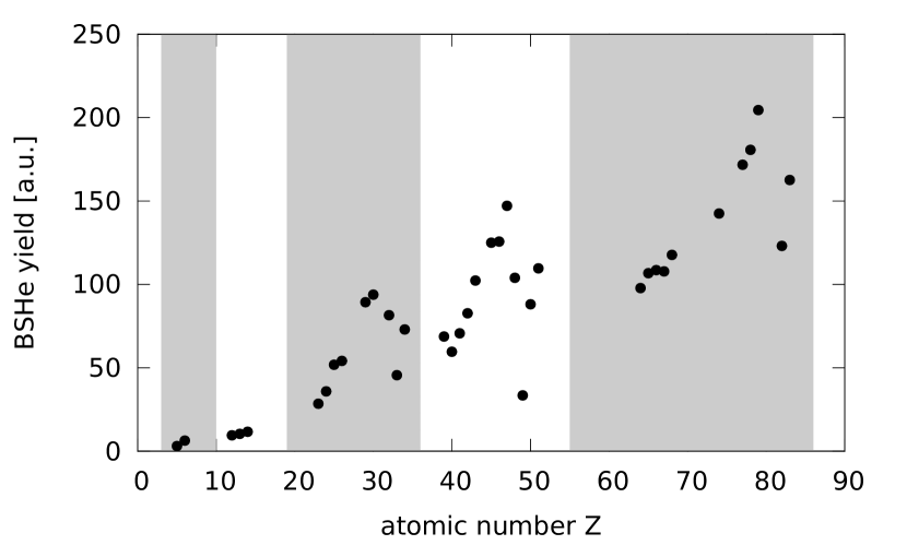
The dependence of the yield on the structure of the periodic table is clearly present.
At this point it is important to realize that a high sensitivity is needed from the detector that is used. Under standard imaging conditions in HIM, typically 500 or less ions are used per pixel. Assuming a high backscatter yield of 20% and taking into account the detector solid angle, no more than 50 ions will reach the detector. A large fraction of these backscattered He particles are also neutralBehan et al. (2010) due a charge transfer process which occurs once they enter the sample. However, this would represent an ideal case for a heavy element bulk target. In practice these numbers can be substantially smaller and not a single ion should be lost in the detector.Hlawacek et al. (2013)
One should realize that contrary to the electrons discussed in the previous section, BSHe represent a bulk signal. Depending on the atomic number sampling depth, between a few tens of nanometers and a few hundred nanometers can be achieved. As can be seen from equ. (5), the backscatter efficiency can be increased by lowering the acceleration voltage. As a side effect, this will also reduce the range of the helium and thus the sampling depth.
In addition to the qualitative element distribution, also quantitative information on the elemental composition can be obtained. For a binary collision—when momentum and energy are conserved—the kinetic energy of the backscattered helium
| (6) |
depends on the on the ratio of the masses of the impinging () and target () particle. Measuring the energy loss at a fixed angle allows the mass of the collision partner, as well as its position relative to the sample surface, to be determined. At high keV or low MeV energies this is known as Rutherford Backscatter Spectroscopy (RBS). This method is known to deliver high sensitivity and excellent depth-resolution. The nature of the involved square function makes the method very sensitive to differences between light elements. A silicon drift detector with a resolution of approximately 4 kV can be used for this purpose. However, due to the relatively low primary energy of only 35 keV, the measured peaks are not as well defined as in classical RBS. Nevertheless, the nature of HIM allows such spectra from areas of only several µm2 to be obtained.Behan et al. (2012) The technique has been successfully applied to measure ZrO2 layer thicknesses on Si substrates with monolayer sensitivitySijbrandij et al. (2010) and for thickness measurements of cobalt/nickel nano–rings.Behan et al. (2012)
The achievable resolution is not only limited by the detector. As a result of the already low primary energy, the backscattered particles have a high probability to undergo multiple scattering events. This occurs for the impinging, as well the backscattered helium particle. Consequently, a statistical broadening of the exit energies of the BSHe exists. It has been shown by simulations that even for an ideal combination, such as a 75 nm thick heavy hafnium oxide film on silicon, an intrinsic uncertainty of 14% exists for the depth resolution of Hf. Given the current detector resolution this value is further increased to 60%.van Gastel et al. (2013) Compositional characterization will have even larger errors due to a severe peak overlap.Behan et al. (2012)
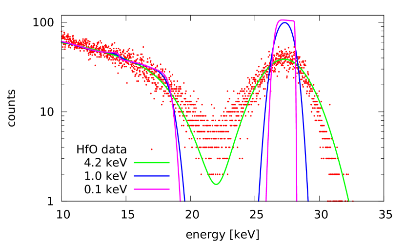
Figure 5 presents an experimentally obtained spectrum from hafnium oxide. The SIMNRAMayer (1999); Sijbrandij et al. (2010) calculated fits to obtain elemental composition and layer thickness have been added for different real and ideal detector resolutions. An increase of detector resolution to 1 kV would substantially improve the quality of the obtained spectra and consequently of the fit accuracy. These curves should be taken to be an indication of what could be possible and not an exact representation of the achievable resolution. One also needs to keep in mind that the majority of the backscattered particles are neutral,Behan et al. (2010); Arafah et al. (1989) complicating any post scattering treatment.
The yield of both signals—secondary electrons as well as back scattered helium—also depends on the crystalline orientation of the sample with respect to the beam. This allows for two additional contrast mechanisms in HIM. The well known channeling contrastBell (2009); Petrov, Vyvenko, and Bondarenko (2010) can be exploited to obtain the crystal orientation of samples with a large lateral resolution.Veligura et al. (2012) This technique makes use of calculations of the blocked area fraction, which yields results similar to stereographic projections of channeling minima or Laue back reflection patterns.
One of the surprising results is that despite the very small wavelength of He ions, Scanning Transmission Ion Microscopy (STIM) is possible. Both dark field and bright field images could be recorded in which thickness fringes and line defects could be identified.Notte et al. (2010)
I.2.3 Photons
Generally speaking, ionoluminescence (IL) is a phenomenon of light emission due to the optical transitions of an electronic system which has been excited by ion irradiation. Three main stages can be distinguished in the luminescence process:Marfunin (1979); Götze and Kempe (2009)
-
1.
energy absorption and excitation of the electronic system;
-
2.
system relaxation and energy transfer to the emission centers;
-
3.
transition of the system into the ground state by photon emission.
During sample bombardment with He+ ions, light can be obtained from the excited backscattered neutral He,Kerkdijk and Thomas (1973); Baird, Zivitz, and Thomas (1975) excited sputtered atoms and molecular complexes,van der Weg and Rol (1965); White (1978); Tolk, Tsong, and White (1977) or from the sample material itself.White (1978); Ghose and Hippler (1998) For the case where emission originates from excited species which have left the sample, the spectrum consists of discrete Doppler–broadened lines. These lines corresponds to the optical transitions within atomic (or molecular) orbitals. This light is usually observed at a distance up to a few millimeters from the target surface.White (1978) In the case of organic samples, ionoluminescence reveals the electronic structure of the organic compounds.Pallon et al. (1997)
For the investigation of material properties we are mainly interested in the luminescence from the sample itself. The physics of the emission processes is usually described by considering the sample’s electronic band structure, or by using configuration coordinate diagrams.Marfunin (1979) According to its origin, there are two general types of luminescence: extrinsic and intrinsic.Scherz (1992) In the case of extrinsic luminescence, the light generation is related to the presence of impurity atoms or ions (so–called activators) in the sample material. Depending on their electronic structure, activators can be divided in the following groups:
-
1.
transition metal ions with dn electronic configuration (e.g. Ti3+, Cr3+, Mn2+);
-
2.
ions with s2 - configuration (e.g. Tl+, Pb2+, Sb3+);
-
3.
rare–earth elements (REE2+/3+);
-
4.
actinides (e.g. UO, Cm3+).
Sometimes the presence of a certain impurity (sensitizer) is needed for the luminescence of an activator (for example Ce3+ for activation of Tb3+ ions Hoffman (1971)). As opposed to sensitizers, quenchers suppress light emission from an activator. For example, Fe2+ ions act as quenchers for emission from Mn2+ in apatite.Filippelli and Delaney (1993) At high activator concentrations self–quenching may occur due to resonant absorption processes.
Intrinsic luminescence on the other hand, is emission from the sample material itself. Two cases can be distinguished. First, optical transitions from delocalized states, or in other words the recombination of free electrons from the conduction band with holes in the valence band. This can include direct and indirect transitions. The radiative recombination of free excitons also falls in this category. Second, optical transitions from localized states can also be attributed to intrinsic luminescence. This includes the following processes: recombination of excitons trapped at defect sites (so–called self–trapped excitonsWilliams and Song (1990)), emission from excited defects—known as color centers (e.g. nitrogen–vacancy centers in diamondDoherty et al. (2013)), and transitions of charge carriers from delocalized into localized states. The shape and width of the emission peaks and bands strongly depends on electron–phonon interactions and thermal effects. A strong electron–phonon interaction leads to a Stokes shift and peak broadening. As a result, it is desirable to perform ionoluminescence measurements at cryogenic temperatures, which has not been done to date in HIM.
Since ionoluminescence is in many aspects similar to the cathodoluminescence (CL) phenomenon often observed in scanning electron microscopy (SEM), databases of CL studies can be employed for the interpretation of IL spectra. Ionoluminescence studies are significantly complicated by the fact that an ion beam not only induces light emission, but also directly influences the optical properties of the target due to defect creation. Ion irradiation can lead to target coloration (e.g. in alkali halidesSchwartz (1997)) and enhanced emission, but also quench the luminescence (e.g. semiconductor materialsBoden et al. (2012a)). However, the use of HIM to observe IL phenomena allows these processes to be followed in–situ with a high lateral resolution.
II Microscopy
In this section we will try to give an overview of applications of helium ion microscopy that make use of the special imaging capabilities of the HIM. Although, the high resolution is the most prominent fact that allows for very accurate critical dimension measurements,Postek et al. (2011) many successful applications of HIM make use of other distinct characteristics of HIM. This overview is by no means complete but will attempt to highlight interesting and eventually surprising imaging applications.
II.1 Insulating and biological samples
The use of electrons for charge neutralization enables HIM to obtain high resolution images of insulating, and in particular uncoated, biological samples. In Fig. 6(a) a high resolution HIM image of a butterfly wing is presented.Boden et al. (2012b) The black ground scales of Papilio ulysses and other butterflies are imaged without any prior coating, which allows the smallest features to be identified. The large depth of field in HIM also makes it ideal for creating anaglyphs using different angles for imaging. High precision measurements of otherwise not accessible feature heights are possible this way.Boden et al. (2012b)
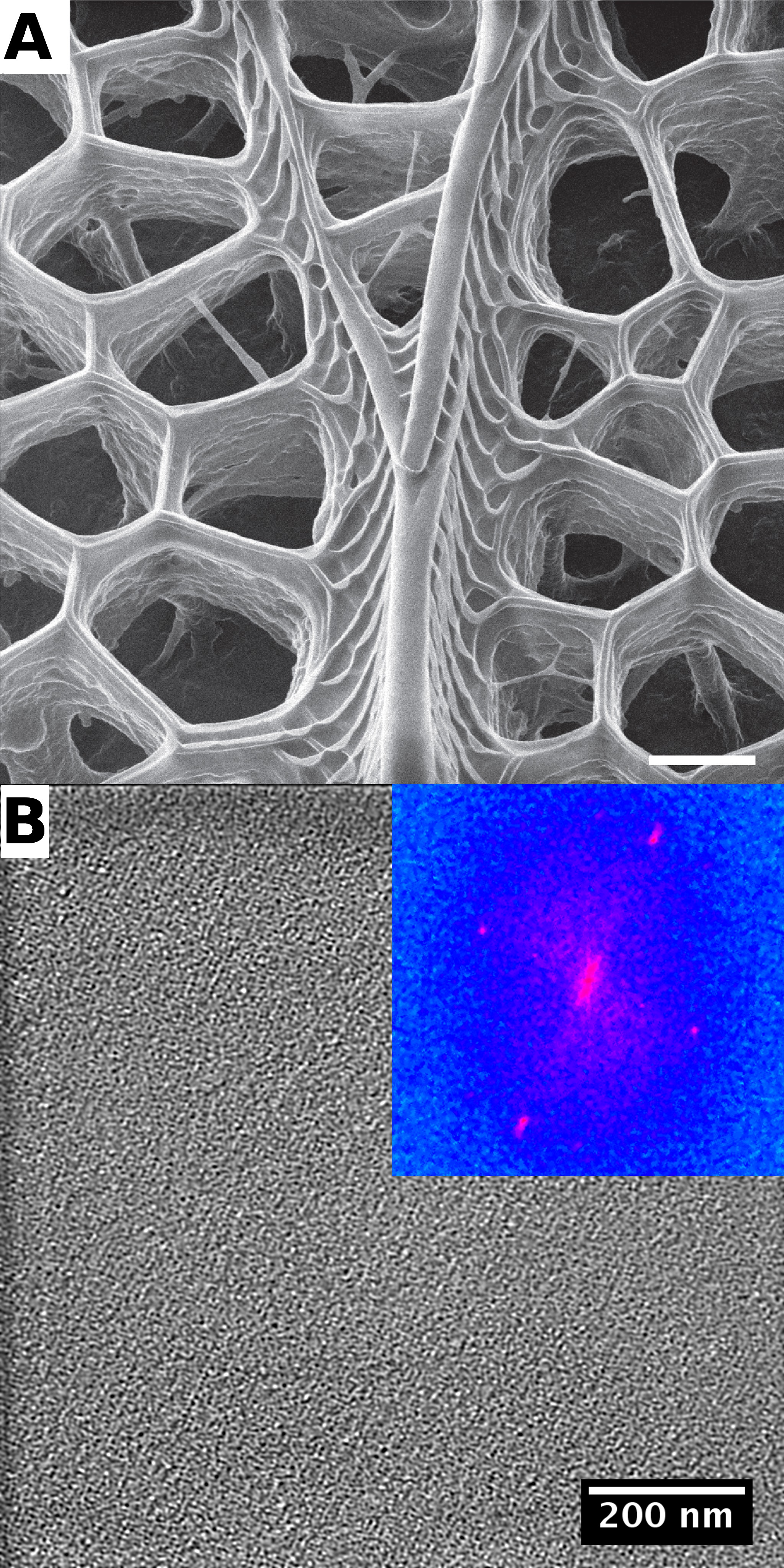
However, only very few groups have demonstrated the applicability of HIM for imaging of cells.Scipioni et al. (2009); Jiang et al. (2010); Joens et al. (2013) This is astonishing since very high resolution should be possible. Figure 6(b) demonstrates the achievable resolution on such biological, soft and insulating samples. The imaged protein crystal (flat bovine liver catalyse) exhibits a simple rectangular unit cell with a lattice spacing of 8.8 nm 6.7 nm. These values are in excellent agreement with the expected values from literature.Luftig (1967)
II.2 Subsurface imaging
The use of BSHe for imaging allows amongst other things subsurface processes such as the formation of buried contacts to be visualized. This overcomes an existing limitation in how we currently try to follow subsurface diffusion processes. Helium ion microscopy offers a unique, destruction free method to reveal the in–plane shape of a diffusion front. In Fig. 7 results of a HIM study on the subsurface formation of Pd interconnects are presented.van Gastel et al. (2012)
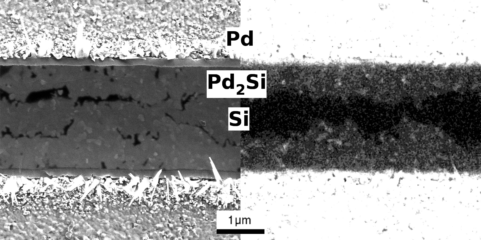
While a large degree of surface detail is present in the SE image presented in Fig. 7(a), no direct indication of the buried Pd2Si interconnect is visible. However, from the simultaneously recorded BSHe image shown in Fig. 7(b) the morphology of the Pd diffusion front can be seen. The benefit of this method over cross section approaches is evident. Besides the obvious ease with which the shape of curved interfaces can be resolved, sample preparation is also substantially easier. Knowledge of the non–straight nature of the diffusion front is important to understand the reason for large variations in device performance. The shape of the subsurface diffusion front is not accessible using cross section techniques. Because the penetration depth of the ions can be varied by using different primary energies, it is also possible to get an estimate of the thickness of the cover layer.van Gastel et al. (2012)
II.3 Ionoluminescence
There are several reviewsWhite (1978); Townsend, Khanlary, and Hole (2007); Townsend (2012) introducing various applications of IL for material characterization that also reveal possible complications of the technique. Here, we will focus on IL imaging with light ions and results obtained with HIM.
The possibility to do IL imaging using a HIM was demonstrated by Boden et al.Boden et al. (2012a) The authors tested a wide range of samples such as quantum dots (QD), semiconductors, rare–earth doped nanocrystals, and Ce3+ doped garnet. Both bulk samples and nanocrystals doped with REE were found to exhibit IL. This is a result of the optical transitions of the electrons in the dopant. However, the IL signal was found to decay with prolonged beam exposure. This decay has been attributed to defect accumulation which hinders electron transport to the actual emitting rare–earth atoms.
Several direct bandgap semiconductor materials were investigated in Ref. [Boden et al., 2012a], but no IL was detected. However, recently we managed to obtain clear ionoluminescence information from such a material. Figure 8 shows the IL image obtained from a thin GaN film on sapphire using a fluence of only cm-2.
The dark lines in the IL image (Fig. 8) are dislocations that are initially present in the film. These act as centers for non–radiative recombinationSugahara et al. (1998) and appear dark. The black dot with the grey halo in the center of the image is the result of the long term irradiation of a single pixel prior to recording the image. Due to the high dose applied there all IL is quenched rapidly. This is the result of the creation of various types of defects that provide non–radiative paths for the electron de–excitation.Kucheyev et al. (2001)
In contrast to bulk semiconductors, the authors of Ref. [Boden et al., 2012a] could record IL images of agglomerates of semiconductor quantum dots. It is suggested, that crystal defects in QDs are generated at a lower rate due to the small size of the particles (5 nm). Hard nuclear collisions occur deeper in the bulk, while in the first tens of nanometers electronic stopping is predominant. The observed emission corresponds to the expected band–gap transition. Nevertheless, the signal is quenched with increasing ion fluence. While QD aggregates were detected with relative ease, attempts to record IL images with higher magnification showing single QDs were not successful.
Alkali halides are known to exhibit intrinsic IL as a result of defect production due to the ion beam radiation.Veligura et al. (2013a); Bazhin, Rausch, and Thomas (1976); Aguilar, Chandler, and Townsends (1979) Figure 9 demonstrates
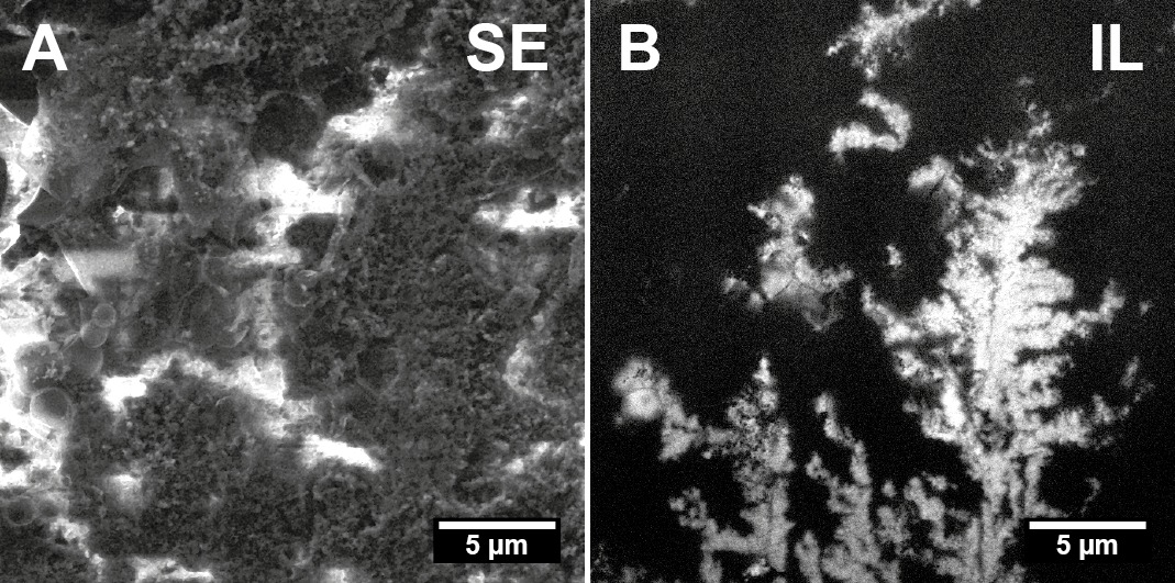
simultaneously acquired images of residues from NaCl solution on a metal substrate. The bright areas in the SE image (Fig. 9(a)) are the aluminum substrate. The darker areas that exhibit a rough appearance are NaCl and residue from the drop–cast solution used. The IL image (Fig. 9(b)) clearly shows the presence of NaCl as bright ramified structures.
Ogawa et al.Ogawa et al. (2012) have reported IL measurements on SiO2 using HIM. Interestingly they observe an increase of the IL intensity with increasing fluence. The authors identify several differences between CL and IL spectra from the same sample, but the nature of the IL signal remains unclear.
The use of IL for analysis of biological samples is possible, but not very often used. The advantage of IL imaging over conventional fluorescence imaging is an absence of diffraction limits that restrict the spatial resolution. In that respect, application of IL in HIM for bio–imaging looks promising. Few groups have used proton beams with energies in the MeV range to investigate biological samples such as cellsWatt et al. (2009) and skin tissue.Pallon et al. (1997) In another study several promising dyes have been identified and can now be used to stain cells specifically for IL investigations.Rossi et al. (2001) However, only limited work is done using IL for imaging of biological samples. Using a classical ion source, a resolution of 150 nm has been demonstrated for ionoluminescence images in STIM mode.Norarat et al. (2013)
II.4 Imaging of thin and soft layers
Graphene, the prototypical thin layer that currently receives a lot of attention, has successfully been imaged by several groups.Lemme et al. (2009); Pickard et al. (2010); Fox et al. (2013); Bell (2009); Nakaharai et al. (2013) This was done for both suspended and free standing graphene. In Fig. 10 a SiO2 supported graphene flake has been imaged using mild imaging conditions.
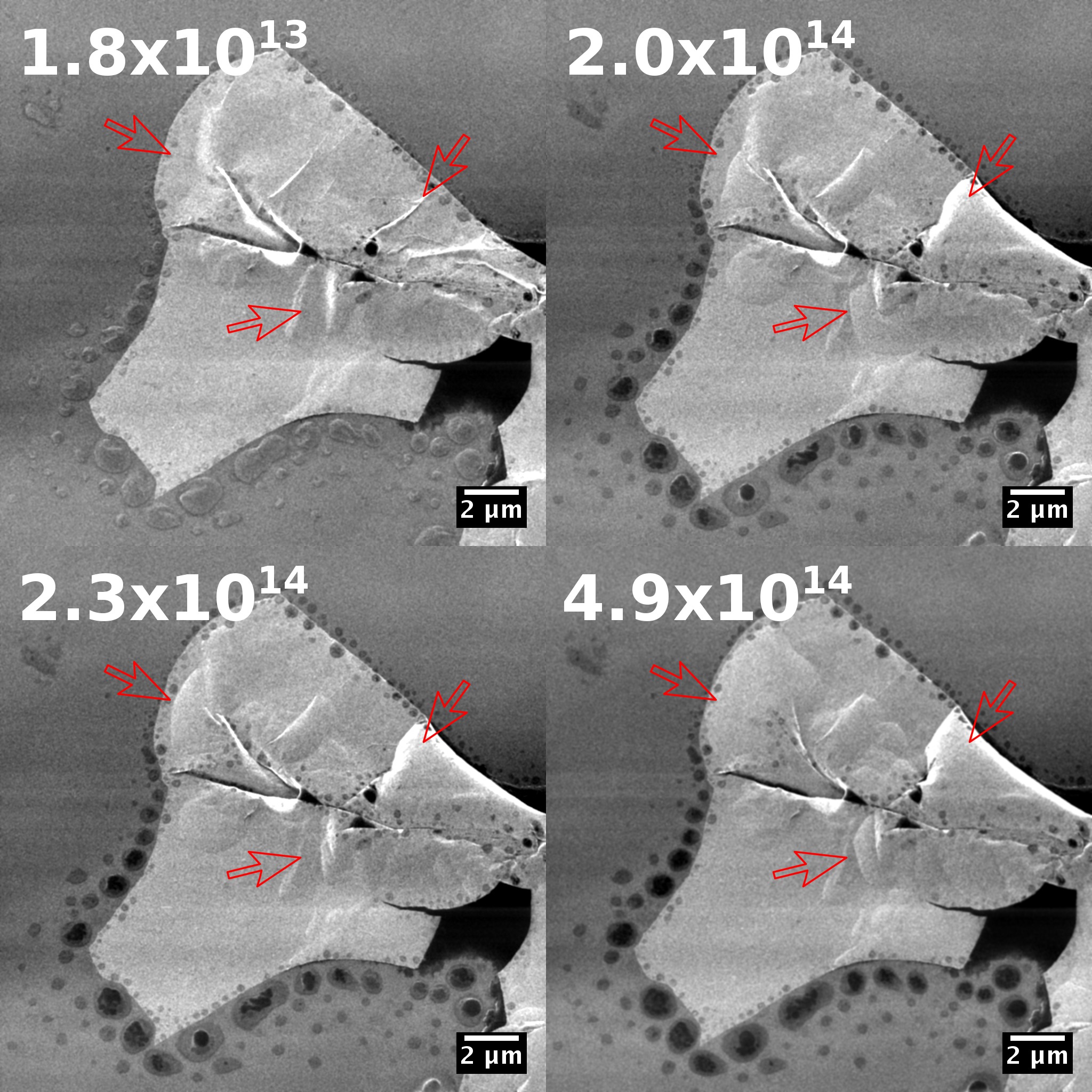
The flakes can be imaged easily with substantial contrast, despite their ultra thin nature. The sequence of images presented in Fig. 10 shows the formation and collapse of helium filled bubbles. Graphene has been shown to be impermeable for many gases including helium,Bunch et al. (2008) hence the backscattered helium remains trapped below the graphene sheet. These bubbles fill with He until either the rim of the flake or a hole in the layer is reached. This will allow the He to escape and the bubble then collapses. This process can be observed for the central bubble between doses of 2.0 cm-2 (initial filling) and 2.3 cm-2 (collapse and start of refilling). The filling of the bubbles and subsequent deformation of the graphene sheet results in the stretching of wrinkles and folds that are present in the sheet. Assuming that the bubble has the shape of a spherical cap with a height of 100 nm and a diameter of 4 µm we can calculate the pressure under the graphene sheet. Using the ideal gas law and a backscatter yield of 0.006, as obtained from SRIMZiegler, Biersack, and Ziegler (2008), we arrive at a pressure on the order of 10 mbar. This value agrees reasonably well with the observed pressure range for gas bubbles under graphene on SiO2 obtained elsewhere.Bunch et al. (2008)
First principles calculations indicate that it should be possible to reveal the graphene lattice using HIM due to minute changes in the electron emission across the lattice.Zhang, Miyamoto, and Rubio (2012) However, the realization of such an image might be difficult due to the destructive nature of the helium beam. It is not clear if sufficient signal can be collected before the defects will alter the local atomic configuration.Fox et al. (2013) Defects created in graphene due to the ion–graphene interaction have been investigated theoretically.Lehtinen et al. (2011); Ålgren et al. (2012); Lehtinen et al. (2010) Recent experimental investigations indicate that already at very low doses severe damage is done to the graphene sheet and many defects are created.Fox et al. (2013) Safe imaging doses for suspended graphene seem to be as low as 1013 to 1014 cm-2.Fox et al. (2013) For supported graphene, as shown above, the critical dose is certainly lower due to the more destructive nature of recoils from the support material.
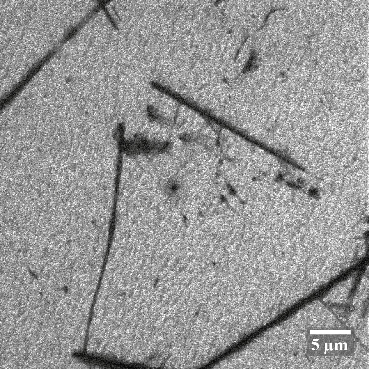
An exceptional imaging result has been achieved for carbon nano membranes (CNM).Turchanin and Gölzhäuser (2012) Such free standing membranes, that are formed by cross linking self–assembled monolayers and then removing the substrate, are difficult to image using conventional SEM. However, in HIM these CNMs are not only visible, but morphological details such as folds and nanometer sized holes created by slow highly charged ions, are also visible.Ritter et al. (2013)
Given the nature of ultra thin films and the sampling volume of the available secondary imaging particles in HIM, the SEs are the obvious choice for imaging such samples. An example of the successful application of HIM to soft layers is the visualization of the phase separation in a mixed poly(3-hexylthiophene)/[6,6]-phenyl-C61-butric acid methyl ester (P3HT/PCBM).Pearson et al. (2011) Such blends are typically used in organic photovoltaic solar cells and represent an important materials class. Although both molecules are essentially carbon, the different number of and bonds in the two polymers results in minute changes of the SE yield.Kishimoto et al. (1990) An other example is the clear identification of self–assembled monolayers (SAM) deposited onto SiO2.Hlawacek et al. (2012); George et al. (2012) Here, differences in work function allow the identification of SAM molecules and give rise to the observed contrast.
A delicate method of visualizing non–continuous ultra thin layers and their different properties utilizes BSHe. For a substrate oriented in a channeling condition, a very low BSHe signal is recorded due to the extended range of He along the low index channeling direction.Veligura et al. (2012) However, at places where a thin surface layer with different atomic positions is present, scattering will occur and an increased BSHe signal can be observed. Although the relative mass of the elements in the adlayers and the underlying bulk are important, this effect works for any combination of bulk and adlayer elements.Mocking, Hlawacek, and Zandvliet (2012) In particular it works for light elements on a heavy substrate.Hlawacek et al. (2012); George et al. (2012)
II.5 Voltage contrast
Similar to SEM, local electromagnetic fields in the sample will influence the yield, angular distribution and energy of the generated SE. This can be utilized to image dopant distributionJepson et al. (2009) and electronic potential distribution. A similar application utilizes static capacitiveUra and Aoyagi (2000) contrast to reveal conducting features buried below an insulating cover.Scipioni et al. (2009)
III Materials modification
The availability of different gases for GFIS—such as NeonRahman et al. (2012); Livengood et al. (2011)—and the combination with a classic liquid metal Gallium Focused Ion Beam (FIB)Notte (2012); Wu et al. (2013) makes the technique interesting for various types of materials modifications. The fine beam produced by the GFIS has the potential to engineer structures with a length scale that is well below what is currently possible with LMIS based FIB techniques. Contrary to e–beam writing, which can achieve similar critical lengths, the removal of material is also possible.
III.1 Resist patterning
Writing structures into resists is usually done using gas injection systems (GIS) in FIB or, if higher resolutions are needed, by using e–beam lithography. In particular the latter suffers from the so–called proximity effect.Chang (1975) The deposition parameters necessary to achieve a constant feature size will depend on the distance to the next feature in the proximity of the beam. This effect is a consequence of the relatively large lateral range of the electrons in the resist material. Structures produced by low mass ion beams are less sensitive to this effect.Itakura, Horiuchi, and Yamamoto (1985) The near complete absence of this effect is related to the fact that in the surface near region there is practically no scattering when using ion beams (see also Fig. 2). Furthermore, very little backscattering occurs in the usually relatively light resist materials. In addition the very low energy SE (<10 eV)Petrov and Vyvenko (2011); Ramachandra, Griffin, and Joy (2009); Ohya et al. (2009); Petrov, Vyvenko, and Bondarenko (2010) in HIM are localized close to the beam path, whereas the SEs in e–beam lithography have a higher energy (>100 eV) and therefore travel relatively long distances in the resist material.Seah and Dench (1979) As a consequence resist modification by ions happens only in a very small volume along the beam path. An extensive overview comparing electrons and ions for their useful application in lithography is given by Melngailis.Melngailis (1993)
With the availability of He GFIS new standards have been set in terms of achievable line width.Winston et al. (2009); Maas et al. (2010); van der Drift and Maas (2012); Alkemade et al. (2012) This has at least partially been made possible by the above discussed, near complete, absence of the proximity effect when using a highly focused He beam. However, to date resists initially developed for e–beam lithography such as hydrogen sylsesquioxane (HSQ) and polymethyl methacrylate resist (PMMA) are used. New resist materials optimized for the large amount of energy deposited by the ion beam could potentially lead to even better results.
III.2 Beam induced deposition
Several precursor materials have been explored including MeCpPtMe3, TEOS, and XeF2.Chen et al. (2010); Maas et al. (2010); Scipioni et al. (2011); Alkemade and van Veldhoven (2012); Sanford et al. (2009) Recently, also a tungsten based metal precursors has successfully been used.Kohama et al. (2013) With this extremely flexible method a wide range of features can be directly sculpted including 3D structures. Figure 11 shows examples of structures created using Ion Beam Induced Deposition (IBID) in the group of P. Alkemade.Alkemade et al. (2012)
However, a detailed understanding of the deposition process is needed to unleash the full potential of the method for resist patterning. A model has been proposed that identifies primary ions and secondary electrons as being responsible for the vertical growth of the structures. Scattered ions and recoil atoms on the other hand are responsible for the lateral growth of the structures.Alkemade et al. (2010) Simulation software (EnvisION) based on this model is available and can be used to predict the metal deposition process in HIM.Chen et al. (2010) The program is based on available concepts and code of an electron–beam–induced simulationSmith, Fowlkes, and Rack (2008) and the IONiSERamachandra, Griffin, and Joy (2009) Monte Carlo program. Experimental confirmation of results showed the applicability of the simulation method.Chen et al. (2010)
III.3 Direct write lithography
Different from what has been discussed in the previous section, here we will discuss structuring results that do rely on the sputtering of sample atoms. Sputtering is a well known phenomenon that has been extensively studied.Sigmund (1987); Thompson (1981); Behrisch and Eckstein (2007) However, with only a few exceptions these works usually focus on ions of lower energies of only a few hundred eV to a few keV for the relevant gases Helium and Neon. For higher energy ranges the bombardment species is either not a noble gas or generally a heavier element. The energy range of interest for HIM is not so well investigated. Surprisingly, many as yet unexplained phenomena, such as very high and fluence dependent sputter yields are observed.Fowley et al. (2013) Due to the sub nanometer size and the collimated nature of the HIM ion beam, it is possible to mill features with very small critical dimensions not possible with current FIB technology. We start by discussing results obtained on the most simple milled structure—a pore. Such pores are successfully used for biomolecule detection. The achievable diameter can be as small as 4 nm, which is 60% smaller compared to other one step milling techniques.Yang et al. (2011) Most importantly the quality of these pores for biomolecule detection is comparable to state–of–the–art pores fabricated using TEMStorm et al. (2005) or FIB.Li et al. (2001) However, these techniques create smallest pores by closing existing bigger pores in a controlled way. The method relies on the fluidization of the material under irradiation and subsequent deformation which is driven by the surface tension and diffusion of ad–atoms created by an ion beam.Storm et al. (2005); Li et al. (2001) Although it has not been demonstrated to date, this should also be possible by careful implantation of He into the area surrounding the pore. In addition to the effects observed elsewhere,Storm et al. (2005); Li et al. (2001) an additional volume increase and subsequent reduction of pore size can occur due to the formation of nano-sized He bubbles.Veligura et al. (2013b); Fox et al. (2012) Substantial redistribution of unsputtered material has already been observed when milling bigger pores.Marshall, Yang, and Hall (2012) As a result, comparable diameters should be achievable.
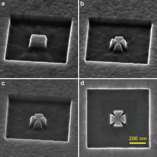
Recently a GFIS using NeonTan et al. (2010) became available. Its combination with a classical liquid metal Gallium FIB column allows for efficient milling of structures at several length scales.Notte (2012) Figure 12 shows a structure milled into gold using all three beams. While initial cut outs are made using the LMIS gallium source (Fig. 12(a)) finer details are cut using the GFIS and Neon (Fig. 12(b)). Smallest details with a length scale of the order of 10 nm are patterned using helium and the GFIS (Fig. 12(c)). The same gas source combination is also used for imaging of the structures.
Another exciting application of helium ion beams for direct write lithography is the successful preparation of devices based on graphene.Boden et al. (2011) The possibility to precisely cut graphene with nanometer precision has been demonstrated earlier by Lemme et al.Lemme et al. (2009) Unfortunately, the unique properties of graphene are very sensitive to damage introduced by the impinging ions.Lucchese et al. (2010) Consequently, only very small fluences of the order of cm-2 can be used to image graphene without damaging it to the extent that the unique properties are lost.Fox et al. (2013) Unfortunately, this excludes high resolution imaging of supported as well as free standing graphene.
III.4 Helium implantation and defect engineering
Helium implantation is unavoidable in HIM. It is therefore important to understand the associated defect structures, their evolution and response to external influences. It has to be made clear that the phenomena discussed in this section appear at doses higher than those normally used in HIM imaging. However, special applications (BSHe or IL imaging) may require relatively high doses. Obviously, He implantation plays an important role when the HIM is used for materials modification, as discussed in the previous section. A dramatic example is shown in Ref. [Wang et al., 2012] in the context of the fabrication of domain wall magnetoresistance devices. Although successful fabrication of domain wall magnetoresistance devices was demonstrated at lower doses, at higher doses the implanted He leads to a swelling and surface deformation that in turn results in the destruction of the patterned devices.
Initial studies that allow the comparison of experimental damage volumes with SRIM were made by Livengood et al.Livengood et al. (2009) One of the results in this publication is summarized in an overview over the different damage regimes that are to be expected for a wide range of He doses (see Fig. 13).
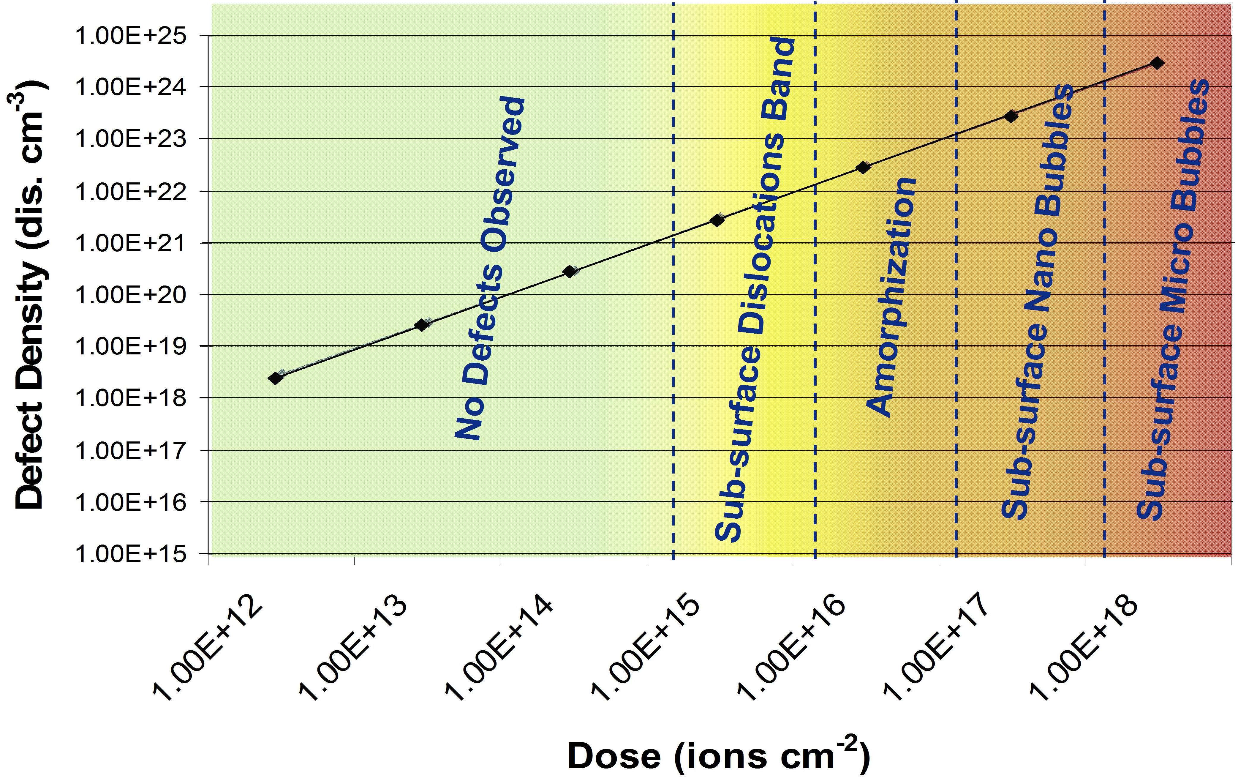
Interestingly, this diagram is valid for both semiconductor materials (silicon) and metals (copper). The validity of these damage regimes has been demonstrated by several groups. A nice visualization of the bubbles that form at depths comparable to the range of the ions in the material is shown by Ref. [Fox et al., 2012]. The pressure inside these bubbles and blisters is high. For the rather soft and ductile metal gold, pressures of up to several GPa can be reached in the initial He nano–bubbles.Veligura et al. (2013b) These bubbles form at open volume defects that are either present in the material or are created by the beam.Laakmann, Jung, and Uelhoff (1987); Rajainmäki et al. (1988) The growth of these initial, nano–sized, He bubbles is independent of the primary energy and leads to observable materials modification at fluences in the low 1017 cm-2 range.Livengood et al. (2009); Veligura et al. (2013b) However, with increasing He dose these bubbles start to coalesce, provided they are formed deep enough in the sample to not immediately reach the sample surface. What follows is a rapid expansion of a blister on the surface. The pressure inside such a blister of a few hundred MPaVeligura et al. (2013b); Wang et al. (2012) is substantially lower than in the initial nano–sized bubbles. The effective formation and rapid growth of He induced blisters is at least partly due to the fact that highly compressed He gas is an ideal stopping medium for He. This results in an amplification of the damage in the vicinity of the bubble and the observed accelerated growth.
IV Summary
In the past half decade Helium Ion Microscopy has proven to be an interesting alternative to its direct and well established competitors: scanning electron microscopy and gallium focused ion beam. However, the authors strongly believe, and hope to have demonstrated above, that HIM is more than a replacement for SEM and FIB. It excels over SEM and FIB in particular for
-
•
high resolution imaging of uncoated biological samples
-
•
imaging of insulating samples
-
•
a high surface sensitivity
-
•
imaging of ultra thin layers
-
•
materials modification with unprecedented resolution
-
•
direct write lithography
-
•
resist patterning
At the same time new applications and techniques are constantly being developed and refined. In particular, analytical additions are needed and are currently being developed. While ionoluminescence has its special applications, additions such as secondary ion mass spectroscopyWirtz et al. (2012) still need to prove their applicability in real materials science problems. However, although spectroscopy is currently still in its infancy, the extension of the technique to other gases such as neon, and potentially even heavier ones, guarantees an exciting future of the technique in particular for nano–fabrication applications.
Acknowledgements.
This research is supported by the Dutch Technology Foundation STW, which is the applied science division of NWO, and the Technology Programme of the Ministry of Economic Affairs.References
- Tondare (2005) V. N. Tondare, “Quest for high brightness, monochromatic noble gas ion sources,” J. Vac. Sci. Technol. A 23, 1498 (2005).
- Bischoff (2005) L. Bischoff, “Alloy liquid metal ion sources and their application in mass separated focused ion beams,” Ultramicroscopy 103, 59–66 (2005).
- Hanssen et al. (2008) J. L. Hanssen, S. B. Hill, J. H. Orloff, and J. J. McClelland, “Magneto–Optical–Trap–Based, high brightness ion source for use as a nanoscale probe.” Nano Lett. 8, 2844–2850 (2008).
- Ji et al. (2002) Q. Ji, X. Jiang, T.-J. King, K.-N. Leung, K. Standiford, and S. B. Wilde, “Improvement in brightness of multicusp-plasma ion source,” J. Vac. Sci. Technol. B 20, 2717 (2002).
- Goldstein et al. (2003) J. I. Goldstein, D. E. Newbury, D. C. Joy, C. E. Lyman, P. Echlin, E. Lifshin, L. Sawyer, and J. R. Michael, Scanning Electron Microscopy and X-ray Microanalysis, 3rd ed. (Springer, Berlin, 2003).
- Utke, Hoffmann, and Melngailis (2008) I. Utke, P. Hoffmann, and J. Melngailis, “Gas-assisted focused electron beam and ion beam processing and fabrication,” J. Vac. Sci. Technol. B 26, 1197 (2008).
- Knoll and Ruska (1932) M. Knoll and E. Ruska, “Das Elektronenmikroskop,” Zeitschrift für Phys. 78, 318–339 (1932).
- Orloff and Swanson (1979) J. H. Orloff and L. W. Swanson, “Angular intensity of a gas-phase field ionization source,” J. Appl. Phys. 50, 6026 (1979).
- Horiuchi, Itakura, and Ishikawa (1988a) K. Horiuchi, T. Itakura, and H. Ishikawa, “Emission characteristics and stability of a helium field ion source,” J. Vac. Sci. Technol. B Microelectron. Nanom. Struct. 6, 937 (1988a).
- Sato (1992) M. Sato, “Current–Pressure Characteristics of Ar Field Ion Source at High Pressures,” Jpn. J. Appl. Phys. 31, L291–L292 (1992).
- Escovitz, Fox, and Levi-Setti (1975) W. H. Escovitz, T. R. Fox, and R. Levi-Setti, “Scanning transmission ion microscope with a field ion source.” Proc. Natl. Acad. Sci. USA 72, 1826–8 (1975).
- Orloff and Swanson (1975) J. H. Orloff and L. W. Swanson, “Study of a field-ionization source for microprobe applications,” J. Vac. Sci. Technol. 12, 1209 (1975).
- Itakura, Horiuchi, and Yamamoto (1985) T. Itakura, K. Horiuchi, and S. Yamamoto, “Focusing column for helium field ion source,” Microelectron. Eng. 3, 153–160 (1985).
- Horiuchi, Itakura, and Ishikawa (1988b) K. Horiuchi, T. Itakura, and H. Ishikawa, “Fine pattern lithography using a helium field ion source,” J. Vac. Sci. Technol. B 6, 241 (1988b).
- Müller (1951) E. W. Müller, “Das Feldionenmikroskop,” Zeitschrift für Phys. 131, 136–142 (1951).
- Melmed (1996) A. J. Melmed, “Recollections of Erwin Müller’s laboratory: the development of FIM (1951–1956),” Appl. Surf. Sci. 94-95, 17–25 (1996).
- Ward, Notte, and Economou (2006) B. W. Ward, J. A. Notte, and N. P. Economou, “Helium ion microscope: A new tool for nanoscale microscopy and metrology,” J. Vac. Sci. Technol. B 24, 2871 (2006).
- Kalbitzer (2004) S. Kalbitzer, “Optimised operation of gas field ion source,” Appl. Phys. A 79, 1901–1905 (2004).
- Pitters et al. (2013) J. L. Pitters, R. Urban, C. Vesa, and R. A. Wolkow, “Tip apex shaping of gas field ion sources.” Ultramicroscopy 131, 56–60 (2013).
- Urban, Wolkow, and Pitters (2012) R. Urban, R. A. Wolkow, and J. L. Pitters, “Field ion microscope evaluation of tungsten nanotip shape using He and Ne imaging gases.” Ultramicroscopy 122, 60–64 (2012).
- Urban, Pitters, and Wolkow (2012) R. Urban, J. L. Pitters, and R. A. Wolkow, “Gas field ion source current stability for trimer and single atom terminated W(111) tips,” Appl. Phys. Lett. 100, 263105 (2012).
- Pitters, Urban, and Wolkow (2012) J. L. Pitters, R. Urban, and R. A. Wolkow, “Creation and recovery of a W(111) single atom gas field ion source.” J. Chem. Phys. 136, 154704 (2012).
- Rahman et al. (2013) F. H. M. Rahman, J. A. Notte, R. H. Livengood, and S. Tan, “Observation of synchronized atomic motions in the field ion microscope.” Ultramicroscopy 126, 10–18 (2013).
- Orloff, Utlaut, and Swanson (2003) J. H. Orloff, M. Utlaut, and L. W. Swanson, High Resolution Focused Ion Beams: FIB and its Applications (Springer US, Boston, MA, 2003).
- Rose (2009) H. H. Rose, Geometrical Charged-Particle Optics, Springer Series in Optical Sciences, Vol. 142 (Springer, Berlin, 2009).
- Ernst et al. (1993) N. Ernst, G. Bozdech, H. Schmidt, W. Schmidt, and G. L. Larkins, “On the full-width-at-half-maximum of field ion energy distributions,” Appl. Surf. Sci. 67, 111–117 (1993).
- Hill, Notte, and Ward (2008) R. Hill, J. A. Notte, and B. W. Ward, “The ALIS He ion source and its application to high resolution microscopy,” Phys. Procedia 1, 135–141 (2008).
- Notte et al. (2007) J. A. Notte, B. W. Ward, N. P. Economou, R. Hill, R. Percival, L. Farkas, S. McVey, D. G. Seiler, A. C. Diebold, R. McDonald, C. M. Garner, D. Herr, R. P. Khosla, and E. M. Secula, “An Introduction to the Helium Ion Microscope,” in AIP Conf. Proc., Vol. 931, edited by D. G. Seiler, A. C. Diebold, R. McDonald, C. M. Garner, D. Herr, R. P. Khosla, and E. M. Secula (AIP, 2007) pp. 489–496.
- Petrov and Vyvenko (2011) Y. V. Petrov and O. F. Vyvenko, “Secondary electron emission spectra and energy selective imaging in helium ion microscope,” in Proc. SPIE, Vol. 8036, edited by J. T. Thomas, D. D. Desjardins, J. J. Güell, and K. L. Bernier (SPIE, Orlando, Florida, 2011) pp. 80360O–1–80360O–10.
- Ramachandra, Griffin, and Joy (2009) R. Ramachandra, B. J. Griffin, and D. C. Joy, “A model of secondary electron imaging in the helium ion scanning microscope,” Ultramicroscopy 109, 748–757 (2009).
- Bell (2009) D. C. Bell, “Contrast mechanisms and image formation in helium ion microscopy.” Microsc. Microanal. 15, 147–53 (2009).
- Scipioni et al. (2009) L. Scipioni, C. A. Sanford, J. A. Notte, B. Thompson, and S. McVey, “Understanding imaging modes in the helium ion microscope,” J. Vac. Sci. Technol. B 27, 3250 (2009).
- Bethe (1941) H. A. Bethe, “Minutes of the Washington, D. C., Meeting May 1-3, 1941,” Phys. Rev. 59, 913–945 (1941).
- Ohya et al. (2008) K. Ohya, K. Inai, A. Nisawa, and A. Itoh, “Emission statistics of X-ray induced photoelectrons and its comparison with electron- and ion-induced electron emissions,” Nucl. Instrum. Meth. B 266, 541–548 (2008).
- Rösler (1985) M. Rösler, “Theory of ion–induced kinetic electron emission from solids,” in Ioniz. Solids by Heavy Part., NATO ASI Series, edited by R. A. Baragiora (Plenum, New York, 1985) pp. 27–58.
- Lin and Joy (2005) Y. Lin and D. C. Joy, “A new examination of secondary electron yield data,” Surf. Interface Anal. 37, 895–900 (2005).
- Ferrón et al. (1981) J. Ferrón, E. Alonso, R. Baragiola, and A. Oliva-Florio, “Dependence of ion-electron emission from clean metals on the incidence angle of the projectile,” Phys. Rev. B 24, 4412–4419 (1981).
- Ohya et al. (2009) K. Ohya, T. Yamanaka, K. Inai, and T. Ishitani, “Comparison of secondary electron emission in helium ion microscope with gallium ion and electron microscopes,” Nucl. Instrum. Meth. B 267, 584–589 (2009).
- Petrov, Vyvenko, and Bondarenko (2010) Y. V. Petrov, O. F. Vyvenko, and A. S. Bondarenko, “Scanning helium ion microscope: Distribution of secondary electrons and ion channeling,” J. Surf. Investig. 4, 792–795 (2010).
- Riccardi et al. (2000) P. Riccardi, P. Barone, A. Bonanno, A. Oliva, and R. Baragiola, “Angular Studies of Potential Electron Emission in the Interaction of Slow Ions with Al Surfaces,” Phys. Rev. Lett. 84, 378–381 (2000).
- Hlawacek et al. (2013) G. Hlawacek, I. Ahmad, M. A. Smithers, and E. S. Kooij, “To see or not to see: Imaging surfactant coated nano-particles using HIM and SEM.” Ultramicroscopy 135C, 89–94 (2013), arXiv:1304.7167 .
- Buchholt et al. (2011) K. Buchholt, P. Eklund, J. Jensen, J. Lu, A. L. Spetz, and L. Hultman, “Step-flow growth of nanolaminate Ti3SiC2 epitaxial layers on 4H-SiC(0001),” Scr. Mater. 64, 1141–1144 (2011).
- Behan et al. (2012) G. Behan, D. Zhou, M. Boese, R. M. Wang, and H. Z. Zhang, “An Investigation of Nickel Cobalt Oxide Nanorings Using Transmission Electron, Scanning Electron and Helium Ion Microscopy,” J. Nanosci. Nanotechnol. 12, 1094–1098 (2012).
- Fox et al. (2013) D. Fox, Y. B. Zhou, A. O’Neill, S. Kumar, J. J. Wang, J. N. Coleman, G. S. Duesberg, J. F. Donegan, and H. Z. Zhang, “Helium ion microscopy of graphene: beam damage, image quality and edge contrast.” Nanotechnology 24, 335702 (2013).
- van Gastel et al. (2011) R. van Gastel, L. Barriss, C. A. Sanford, G. Hlawacek, L. Scipioni, A. Merkle, D. Voci, C. Fenner, H. J. W. Zandvliet, and B. Poelsema, “Design and performance of a Near Ultra High Vacuum Helium Ion Microscope,” Microsc. Microanal. 17, 928–929 (2011).
- Veligura et al. (2012) V. Veligura, G. Hlawacek, R. van Gastel, H. J. W. Zandvliet, and B. Poelsema, “Channeling in helium ion microscopy: Mapping of crystal orientation.” Beilstein J. Nanotechnol. 3, 501–506 (2012).
- Behan et al. (2010) G. Behan, J. F. Feng, H. Z. Zhang, P. N. Nirmalraj, and J. J. Boland, “Effect of sample bias on backscattered ion spectroscopy in the helium ion microscope,” J. Vac. Sci. Technol. A 28, 1377 (2010).
- Sijbrandij et al. (2010) S. Sijbrandij, J. A. Notte, L. Scipioni, C. Huynh, and C. A. Sanford, “Analysis and metrology with a focused helium ion beam,” J. Vac. Sci. Technol. B 28, 73 (2010).
- van Gastel et al. (2013) R. van Gastel, G. Hlawacek, S. Dutta, and B. Poelsema, “Backscattered Helium Spectroscopy in the Helium Ion Microscope: Principles, Resolution and Applications,” in IOP Conf. Ser. Mater. Sci. Eng. (European Microbeam Analysis Society, Porto, 2013).
- Mayer (1999) M. Mayer, “SIMNRA, a simulation program for the analysis of NRA, RBS and ERDA,” in AIP Conf. Proc. (AIP, 1999) pp. 541–544.
- Arafah et al. (1989) D.-E. Arafah, J. Meyer, H. Sharabati, and A. Mahmoud, “Charge-state measurements of backscattered ions from Au films,” Phys. Rev. A 39, 3836–3841 (1989).
- Notte et al. (2010) J. A. Notte, R. Hill, S. M. McVey, R. Ramachandra, B. J. Griffin, and D. C. Joy, “Diffraction imaging in a He+ ion beam scanning transmission microscope.” Microsc. Microanal. 16, 599–603 (2010).
- Marfunin (1979) A. S. Marfunin, “Luminescence,” in Spectroscopy, Luminescence and Radiation Centers in Minerals (Springer, Berlin, Heidelberg, 1979) Chap. 5, pp. 141–222.
- Götze and Kempe (2009) J. Götze and U. Kempe, “Physical Principles of Cathodoluminescence (CL) and its Applications in Geosciences,” in Cathodoluminescence and its Application in the Planetary Sciences, Cl, edited by A. Gucsik (Springer, Berlin, 2009) Chap. 1, pp. 1–22.
- Kerkdijk and Thomas (1973) C. Kerkdijk and E. Thomas, “Light emission induced by H+ and He+ impact on a clean copper surface,” Physica 63, 577–598 (1973).
- Baird, Zivitz, and Thomas (1975) W. Baird, M. Zivitz, and E. Thomas, “Excited–state formation as H+ and He+ ions scatter from metal surfaces,” Phys. Rev. A 12, 876–884 (1975).
- van der Weg and Rol (1965) W. F. van der Weg and P. K. Rol, “On the excited state of sputtered particles,” Nucl. Instrum. Methods 38, 274–276 (1965).
- White (1978) C. W. White, “Ion induced optical emission for surface and depth profile analysis,” Nucl. Instrum. Methods 149, 497–506 (1978).
- Tolk, Tsong, and White (1977) N. H. Tolk, I. S. T. Tsong, and C. W. White, “In situ spectrochemical analysis of solid surfaces by ion beam sputtering,” Anal. Chem. 49, 16A–30A (1977).
- Ghose and Hippler (1998) D. Ghose and R. Hippler, “Ionoluminescence,” in Luminescence of Solids, edited by D. R. Vij (Springer US, 1998) pp. 189–220.
- Pallon et al. (1997) J. Pallon, C. Yang, R. Utui, M. Elfman, K. Malmqvist, P. Kristiansson, and K. Sjöland, “Ionoluminescence technique for nuclear microprobes,” Nucl. Instrum. Meth. B 130, 199–203 (1997).
- Scherz (1992) U. Scherz, “Grundlagen der Festkörperphysik,” in Lehrbuch der Experimentalphysik, edited by R. Kassing (Gruyter, Berlin, 1992) 2nd ed., pp. 1–107.
- Hoffman (1971) M. V. Hoffman, “Effect of Thorium on Ce Phosphors,” J. Electrochem. Soc. 118, 1508 (1971).
- Filippelli and Delaney (1993) G. M. Filippelli and M. L. Delaney, “The effects of manganese(II) and iron(II) on the cathodoluminescence signal in synthetic apatite,” SEPM J. Sediment. Res. Vol. 63, 167–173 (1993).
- Williams and Song (1990) R. Williams and K. Song, “The self–trapped exciton,” J. Phys. Chem. Solids 51, 679–716 (1990).
- Doherty et al. (2013) M. W. Doherty, N. B. Manson, P. Delaney, F. Jelezko, J. Wrachtrup, and L. C. Hollenberg, “The nitrogen-vacancy colour centre in diamond,” Phys. Rep. 528, 1–45 (2013).
- Schwartz (1997) K. Schwartz, “Excitons and radiation damage in alkali halides,” in At. Phys. Methods Mod. Res., Lecture Notes in Physics, Vol. 1, edited by K. P. Jungmann, J. Kowalski, I. Reinhard, and F. Träger (Springer, Berlin, 1997) pp. 351–366.
- Boden et al. (2012a) S. A. Boden, T. M. W. Franklin, L. Scipioni, D. M. Bagnall, and H. N. Rutt, “Ionoluminescence in the helium ion microscope.” Microsc. Microanal. 18, 1253–1262 (2012a).
- Postek et al. (2011) M. T. Postek, A. Vladár, C. Archie, and B. Ming, “Review of current progress in nanometrology with the helium ion microscope,” Meas. Sci. Technol. 22, 024004 (2011).
- Boden et al. (2012b) S. A. Boden, A. Asadollahbaik, H. N. Rutt, and D. M. Bagnall, “Helium ion microscopy of Lepidoptera scales.” Scanning 34, 107–120 (2012b).
- Jiang et al. (2010) W. Jiang, V. Shutthanandan, B. Arey, and A. Lea, “Helium Ion Microscopy of Microstructures and Biological Samples,” in Microsc. Microanal. (Portland, 2010).
- Joens et al. (2013) M. S. Joens, C. Huynh, J. M. Kasuboski, D. C. Ferranti, Y. J. Sigal, F. Zeitvogel, M. Obst, C. J. Burkhardt, K. P. Curran, S. H. Chalasani, L. A. Stern, B. Goetze, and J. A. J. Fitzpatrick, “Helium Ion Microscopy (HIM) for the imaging of biological samples at sub–nanometer resolution.” Sci. Rep. 3, 3514 (2013).
- Luftig (1967) R. Luftig, “An accurate measurement of the catalase crystal period and its use as an internal marker for electron microscopy,” J. Ultrastruct. Res. 20, 91–102 (1967).
- van Gastel et al. (2012) R. van Gastel, G. Hlawacek, H. J. W. Zandvliet, and B. Poelsema, “Subsurface analysis of semiconductor structures with helium ion microscopy,” Microelectron. Reliab. 52, 2104–2109 (2012).
- Townsend, Khanlary, and Hole (2007) P. Townsend, M. Khanlary, and D. Hole, “Information obtainable from ion beam luminescence,” Surf. Coatings Technol. 201, 8160–8164 (2007).
- Townsend (2012) P. Townsend, “Variations on the use of ion beam luminescence,” Nucl. Instrum. Meth. B 286, 35–39 (2012).
- Sugahara et al. (1998) T. Sugahara, H. Sato, M. Hao, Y. Naoi, S. Kurai, S. Tottori, K. Yamashita, K. Nishino, L. T. Romano, and S. Sakai, “Direct Evidence that Dislocations are Non-Radiative Recombination Centers in GaN,” Jpn. J. Appl. Phys. 37, L398–L400 (1998).
- Kucheyev et al. (2001) S. O. Kucheyev, M. Toth, M. R. Phillips, J. S. Williams, C. Jagadish, and G. Li, “Cathodoluminescence depth profiling of ion-implanted GaN,” Appl. Phys. Lett. 78, 34 (2001).
- Veligura et al. (2013a) V. Veligura, G. Hlawacek, R. van Gastel, H. J. W. Zandvliet, and B. Poelsema, “High resolution ionoluminescence study of defect creation and interaction,” J. Phys. Condens. Matter , submitted (2013a).
- Bazhin, Rausch, and Thomas (1976) A. Bazhin, E. Rausch, and E. Thomas, “Luminescence induced by ion impact on alkali-halide crystals at high temperatures (-160 to 200°C),” Phys. Rev. B 14, 2583–2591 (1976).
- Aguilar, Chandler, and Townsends (1979) M. Aguilar, P. J. Chandler, and P. D. Townsends, “Luminescence of NaCl—I. Electron and ion beam excited spectra,” Radiat. Eff. 40, 1–7 (1979).
- Ogawa et al. (2012) S. Ogawa, T. Iijima, S. Awata, R. Sugie, N. Kawasaki, and Y. Otsuka, “Characterization of Damage in SiO2 during Helium Ion Microscope Observation by Luminescence and TEM-EELS,” Microsc. Microanal. 18, 814–815 (2012).
- Watt et al. (2009) F. Watt, A. Bettiol, J. V. Kan, M. Ynsa, R. Minqin, R. Rajendran, C. Huifang, S. Fwu-Shen, and A. Jenner, “Imaging of single cells and tissue using MeV ions,” Nucl. Instrum. Meth. B 267, 2113–2116 (2009).
- Rossi et al. (2001) P. Rossi, C. Di Maggio, G. Egeni, A. Galligioni, G. Gennaro, L. Giacomelli, A. Lo Giudice, M. Pegoraro, L. Pescarini, V. Rudello, and E. Vittone, “Cytological and histological structures identification with the technique IBIL in elemental microanalysis,” Nucl. Instrum. Meth. B 181, 437–442 (2001).
- Norarat et al. (2013) R. Norarat, V. Marjomäki, X. Chen, M. Zhaohong, R. Minqin, C.-B. Chen, A. Bettiol, H. Whitlow, and F. Watt, “Ion-induced fluorescence imaging of endosomes,” Nucl. Instrum. Meth. B 306, 113–116 (2013).
- Lemme et al. (2009) M. C. Lemme, D. C. Bell, J. R. Williams, L. A. Stern, B. W. H. Baugher, P. Jarillo-Herrero, and C. M. Marcus, “Etching of graphene devices with a helium ion beam.” ACS Nano 3, 2674–2676 (2009), arXiv:0905.4409 .
- Pickard et al. (2010) D. Pickard, B. Oezyilmaz, J. Thong, K. Loh, V. Viswanathan, A. Zhongkai, S. Mathew, T. Kundu, C. Park, Z. Yi, X. Xu, K. Zhang, T. Tat, H. Wang, and T. Venkatesan, “Graphene Nanoribbons Fabricated by Helium Ion microscope,” in Bull. Am. Phys. Soc., Vol. 55 (American Physical Society, Portland, Oregon, 2010).
- Nakaharai et al. (2013) S. Nakaharai, T. Iijima, S. Ogawa, S. Suzuki, S.-l. Li, K. Tsukagoshi, S. Sato, and N. Yokoyama, “Conduction tuning of graphene based on defect-induced localization.” ACS Nano 7, 5694–5700 (2013).
- Bunch et al. (2008) J. S. Bunch, S. S. Verbridge, J. S. Alden, A. M. van der Zande, J. M. Parpia, H. G. Craighead, and P. L. McEuen, “Impermeable atomic membranes from graphene sheets.” Nano Lett. 8, 2458–2462 (2008).
- Ziegler, Biersack, and Ziegler (2008) J. F. Ziegler, J. P. Biersack, and M. D. Ziegler, SRIM, the stopping and range of ions in matter (SRIM Co., 2008).
- Zhang, Miyamoto, and Rubio (2012) H. Zhang, Y. Miyamoto, and A. Rubio, “Ab initio Simulation of Helium-Ion Microscopy Images: The Case of Suspended Graphene,” Phys. Rev. Lett. 109, 265505 (2012).
- Lehtinen et al. (2011) O. Lehtinen, J. Kotakoski, A. V. Krasheninnikov, and J. Keinonen, “Cutting and controlled modification of graphene with ion beams.” Nanotechnology 22, 175306 (2011).
- Ålgren et al. (2012) E. H. Ålgren, J. Kotakoski, O. Lehtinen, and A. V. Krasheninnikov, “Ion irradiation tolerance of graphene as studied by atomistic simulations,” Appl. Phys. Lett. 100, 233108 (2012).
- Lehtinen et al. (2010) O. Lehtinen, J. Kotakoski, A. V. Krasheninnikov, A. Tolvanen, K. Nordlund, and J. Keinonen, “Effects of ion bombardment on a two-dimensional target: Atomistic simulations of graphene irradiation,” Phys. Rev. B 81, 153401 (2010).
- Turchanin and Gölzhäuser (2012) A. Turchanin and A. Gölzhäuser, “Carbon nanomembranes from self-assembled monolayers: Functional surfaces without bulk,” Prog. Surf. Sci. 87, 108–162 (2012).
- Ritter et al. (2013) R. Ritter, R. A. Wilhelm, M. Stöger-Pollach, R. Heller, A. Mücklich, U. Werner, H. Vieker, A. Beyer, S. Facsko, A. Gölzhäuser, and F. Aumayr, “Fabrication of nanopores in 1 nm thick carbon nanomembranes with slow highly charged ions,” Appl. Phys. Lett. 102, 063112 (2013).
- Pearson et al. (2011) A. J. Pearson, S. A. Boden, D. M. Bagnall, D. G. Lidzey, and C. Rodenburg, “Imaging the bulk nanoscale morphology of organic solar cell blends using helium ion microscopy.” Nano Lett. 11, 4275–4281 (2011).
- Kishimoto et al. (1990) Y. Kishimoto, T. Ohshima, M. Hashimoto, and T. Hayashi, “A consideration of secondary electron emission from organic solids,” J. Appl. Polym. Sci. 39, 2055–2066 (1990).
- Hlawacek et al. (2012) G. Hlawacek, V. Veligura, S. Lorbek, T. F. Mocking, A. George, R. van Gastel, H. J. W. Zandvliet, and B. Poelsema, “Imaging ultra thin layers with helium ion microscopy: Utilizing the channeling contrast mechanism.” Beilstein J. Nanotechnol. 3, 507–512 (2012).
- George et al. (2012) A. George, M. Knez, G. Hlawacek, D. Hagedoorn, H. H. J. Verputten, R. van Gastel, and J. E. ten Elshof, “Nanoscale patterning of organosilane molecular thin films from the gas phase and its applications: fabrication of multifunctional surfaces and large area molecular templates for site-selective material deposition.” Langmuir 28, 3045–3052 (2012).
- Mocking, Hlawacek, and Zandvliet (2012) T. F. Mocking, G. Hlawacek, and H. J. W. Zandvliet, “Cobalt induced nanocrystals on Ge(001),” Surf. Sci. 606, 924–927 (2012).
- Jepson et al. (2009) M. A. E. Jepson, B. J. Inkson, C. Rodenburg, and D. C. Bell, “Dopant contrast in the helium ion microscope,” Europhys. Lett. 85, 46001 (2009).
- Ura and Aoyagi (2000) K. Ura and S. Aoyagi, “Static capacitance contrast of LSI covered with an insulator film in low accelerating voltage scanning electron microscope,” J. Electron Microsc. (Tokyo). 49, 157–162 (2000).
- Rahman et al. (2012) F. H. M. Rahman, S. McVey, L. Farkas, J. A. Notte, S. Tan, and R. H. Livengood, “The prospects of a subnanometer focused neon ion beam.” Scanning 34, 129–134 (2012).
- Livengood et al. (2011) R. H. Livengood, S. Tan, R. Hallstein, J. A. Notte, S. McVey, and F. H. Rahman, “The neon gas field ion source—a first characterization of neon nanomachining properties,” Nucl. Instrum. Meth. A 645, 136–140 (2011).
- Notte (2012) J. A. Notte, “Charged Particle Microscopy: Why Mass Matters,” Micros. Today 20, 16–22 (2012).
- Wu et al. (2013) H. M. Wu, L. A. Stern, J. H. Chen, M. Huth, C. H. Schwalb, M. Winhold, F. Porrati, C. M. Gonzalez, R. Timilsina, and P. D. Rack, “Synthesis of nanowires via helium and neon focused ion beam induced deposition with the gas field ion microscope.” Nanotechnology 24, 175302 (2013).
- Chang (1975) T. H. P. Chang, “Proximity effect in electron-beam lithography,” J. Vac. Sci. Technol. 12, 1271 (1975).
- Seah and Dench (1979) M. P. Seah and W. A. Dench, “Quantitative electron spectroscopy of surfaces: A standard data base for electron inelastic mean free paths in solids,” Surf. Interface Anal. 1, 2–11 (1979).
- Melngailis (1993) J. Melngailis, “Focused ion beam lithography,” Nucl. Instrum. Meth. B 80-81, 1271–1280 (1993).
- Winston et al. (2009) D. Winston, B. M. Cord, B. Ming, D. C. Bell, W. F. DiNatale, L. A. Stern, A. E. Vladar, M. T. Postek, M. K. Mondol, J. K. W. Yang, and K. K. Berggren, “Scanning-helium-ion-beam lithography with hydrogen silsesquioxane resist,” J. Vac. Sci. Technol. B Microelectron. Nanom. Struct. 27, 2702 (2009).
- Maas et al. (2010) D. J. Maas, E. van Veldhoven, P. Chen, V. Sidorkin, H. W. M. Salemink, E. van der Drift, and P. F. A. Alkemade, “Nanofabrication with a helium ion microscope,” in Metrol. Insp. Process Control Microlithogr. XXIV, Vol. 7638, edited by C. J. Raymond (2010) p. 763814.
- van der Drift and Maas (2012) E. van der Drift and D. J. Maas, Nanofabrication: Techniques and principles, edited by M. Stepanova and S. Dew (Springer Vienna, Vienna, 2012) pp. 93–116.
- Alkemade et al. (2012) P. F. A. Alkemade, E. M. Koster, E. van Veldhoven, and D. J. Maas, “Imaging and nanofabrication with the helium ion microscope of the Van Leeuwenhoek Laboratory in Delft.” Scanning 34, 90–100 (2012).
- Chen et al. (2010) P. Chen, E. van Veldhoven, C. A. Sanford, H. W. M. Salemink, D. J. Maas, D. A. Smith, P. D. Rack, and P. F. A. Alkemade, “Nanopillar growth by focused helium ion-beam-induced deposition.” Nanotechnology 21, 455302 (2010).
- Scipioni et al. (2011) L. Scipioni, C. A. Sanford, E. van Veldhoven, and D. J. Maas, “A Design-of-Experiments Approach to Characterizing Beam-Induced Deposition in the Helium Ion Microscope,” Micros. Today 19, 22–26 (2011).
- Alkemade and van Veldhoven (2012) P. F. A. Alkemade and E. van Veldhoven, “Deposition, Milling, and Etching with a Focused Helium Ion Beam,” in Nanofabrication: Techniques and principles, edited by M. Stepanova and S. Dew (Springer, Vienna, 2012) pp. 275—-300.
- Sanford et al. (2009) C. A. Sanford, L. Stern, L. Barriss, L. Farkas, M. DiManna, R. Mello, D. J. Maas, and P. F. A. Alkemade, “Beam induced deposition of platinum using a helium ion microscope,” J. Vac. Sci. Technol. B 27, 2660 (2009).
- Kohama et al. (2013) K. Kohama, T. Iijima, M. Hayashida, and S. Ogawa, “Tungsten-based pillar deposition by helium ion microscope and beam-induced substrate damage,” J. Vac. Sci. Technol. B 31, 031802 (2013).
- Alkemade et al. (2010) P. F. A. Alkemade, P. Chen, E. van Veldhoven, and D. J. Maas, “Model for nanopillar growth by focused helium ion-beam-induced deposition,” J. Vac. Sci. Technol. B 28, C6F22 (2010).
- Smith, Fowlkes, and Rack (2008) D. A. Smith, J. D. Fowlkes, and P. D. Rack, “Simulating the effects of surface diffusion on electron beam induced deposition via a three-dimensional Monte Carlo simulation.” Nanotechnology 19, 415704 (2008).
- Sigmund (1987) P. Sigmund, “Mechanisms and theory of physical sputtering by particle impact,” Nucl. Instrum. Meth. B 27, 1–20 (1987).
- Thompson (1981) M. Thompson, “Physical mechanisms of sputtering,” Phys. Rep. 69, 335–371 (1981).
- Behrisch and Eckstein (2007) R. Behrisch and W. Eckstein, eds., Sputtering by Particle Bombardment, Topics in Applied Physics, Vol. 110 (Springer Berlin Heidelberg, Berlin, Heidelberg, 2007).
- Fowley et al. (2013) C. Fowley, Z. Diao, C. C. Faulkner, J. Kally, K. Ackland, G. Behan, H. Z. Zhang, a. M. Deac, and J. M. D. Coey, “Local modification of magnetic anisotropy and ion milling of Co/Pt multilayers using a He+ ion beam microscope,” J. Phys. D. Appl. Phys. 46, 195501 (2013).
- Yang et al. (2011) J. Yang, D. C. Ferranti, L. A. Stern, C. A. Sanford, J. Huang, Z. Ren, L.-C. Qin, and A. R. Hall, “Rapid and precise scanning helium ion microscope milling of solid-state nanopores for biomolecule detection.” Nanotechnology 22, 285310 (2011).
- Storm et al. (2005) A. J. Storm, J. H. Chen, X. S. Ling, H. W. Zandbergen, and C. Dekker, “Electron-beam-induced deformations of SiO2 nanostructures,” J. Appl. Phys. 98, 014307 (2005).
- Li et al. (2001) J. Li, D. Stein, C. McMullan, D. Branton, M. J. Aziz, and J. A. Golovchenko, “Ion-beam sculpting at nanometre length scales.” Nature 412, 166–9 (2001).
- Veligura et al. (2013b) V. Veligura, G. Hlawacek, R. P. Berkelaar, R. van Gastel, H. J. W. Zandvliet, and B. Poelsema, “Digging gold: keV He+ ion interaction with Au,” Beilstein J. Nanotechnol. 4, 453–460 (2013b).
- Fox et al. (2012) D. Fox, Y. Chen, C. C. Faulkner, and H. Z. Zhang, “Nano-structuring, surface and bulk modification with a focused helium ion beam.” Beilstein J. Nanotechnol. 3, 579–585 (2012).
- Marshall, Yang, and Hall (2012) M. M. Marshall, J. Yang, and A. R. Hall, “Direct and transmission milling of suspended silicon nitride membranes with a focused helium ion beam.” Scanning 34, 101–106 (2012).
- Tan et al. (2010) S. Tan, R. H. Livengood, D. Shima, J. A. Notte, and S. McVey, “Gas field ion source and liquid metal ion source charged particle material interaction study for semiconductor nanomachining applications,” J. Vac. Sci. Technol. B 28, C6F15 (2010).
- Boden et al. (2011) S. A. Boden, Z. Moktadir, D. M. Bagnall, H. Mizuta, and H. N. Rutt, “Focused helium ion beam milling and deposition,” Microelectron. Eng. 88, 2452–2455 (2011).
- Lucchese et al. (2010) M. Lucchese, F. Stavale, E. H. M. Ferreira, C. Vilani, M. Moutinho, R. B. Capaz, C. A. Achete, and A. Jorio, “Quantifying ion-induced defects and Raman relaxation length in graphene,” Carbon N. Y. 48, 1592–1597 (2010).
- Wang et al. (2012) Y. Wang, S. A. Boden, D. M. Bagnall, H. N. Rutt, and C. H. de Groot, “Helium ion beam milling to create a nano-structured domain wall magnetoresistance spin valve.” Nanotechnology 23, 395302 (2012).
- Livengood et al. (2009) R. H. Livengood, S. Tan, Y. Greenzweig, J. A. Notte, and S. McVey, “Subsurface damage from helium ions as a function of dose, beam energy, and dose rate,” J. Vac. Sci. Technol. B 27, 3244 (2009).
- Laakmann, Jung, and Uelhoff (1987) J. Laakmann, P. Jung, and W. Uelhoff, “Solubility of helium in gold,” Acta Metall. 35, 2063–2069 (1987).
- Rajainmäki et al. (1988) H. Rajainmäki, S. Linderoth, H. Hansen, R. Nieminen, and M. Bentzon, “Nucleation and growth of helium bubbles in aluminum between 20 and 900 K,” Phys. Rev. B 38, 1087–1094 (1988).
- Wirtz et al. (2012) T. Wirtz, N. Vanhove, L. Pillatsch, D. Dowsett, S. Sijbrandij, and J. A. Notte, “Towards secondary ion mass spectrometry on the helium ion microscope: An experimental and simulation based feasibility study with He+ and Ne+ bombardment,” Appl. Phys. Lett. 101, 041601 (2012).
- Demers et al. (2011) H. Demers, N. Poirier-Demers, A. R. Couture, D. Joly, M. Guilmain, N. de Jonge, and D. Drouin, “Three-dimensional electron microscopy simulation with the CASINO Monte Carlo software.” Scanning 33, 135–146 (2011).
- Hill and Rahman (2011) R. Hill and F. H. M. Rahman, “Advances in helium ion microscopy,” Nucl. Instrum. Meth. A 645, 96–101 (2011).