Conducting and insulating LaAlO3/SrTiO3 interfaces:
A comparative surface photovoltage investigation
Abstract
Surface photovoltage (SPV) spectroscopy, which is a versatile method to analyze the energetic distribution of electronic defect states at surfaces and interfaces of wide-bandgap semiconductor (hetero-)structures, is applied to comparatively investigate heterostructures made of 5-unit-cell-thick LaAlO3 films grown either on TiO2- or on SrO-terminated SrTiO3. As shown in a number of experimental and theoretical investigations in the past, these two interfaces exhibit dramatically different properties with the first being conducting and the second insulating.
Our present SPV investigation reveals clearly distinguishable interface defect state distributions for both configurations when interpreted within the framework of a classical semiconductor band scheme. Furthermore, bare SrTiO3 crystals with TiO2 or mixed SrO/TiO2 terminations show similar SPV spectra and transients as do LaAlO3-covered samples with the respective termination of the SrTiO3 substrate. This is in accordance with a number of recent works that stress the decisive role of SrTiO3 and the minor role of LaAlO3 with respect to the electronic interface properties.
pacs:
68.08.-p, 68.47.Gh, 71.20.Ps, 71.30+h, 72.20.-i, 72.40.+w, 73.20.-r, 73.40.-c, 73.50.Pz, 73.61.Ng, 77.84.BwI Introduction
Perovskite oxide heterostructures in general and their interface physics in particular have attracted a lot of scientific interest in the past and are one key issue of the highly topical field of oxide electronics, which is dedicated to finding novel material systems and device concepts for micro- and nanoelectronics beyond the conventional semiconductor technology. In this context the LaAlO3/SrTiO3 (LAO/STO) system has been the subject of intense research activities, especially since the publication of Ohtomo and Hwang in 2004 Ohtomo and Hwang (2004), in which the existence of a conducting 2-dimensional electron gas (2-DEG) – in the meantime more frequently characterized as electron liquid (2-DEL) – at the interface between TiO2-terminated SrTiO3 and LaAlO3 thin films was described. The conducting interface occurs only in samples with LAO layers thicker than 4 unit cells and never for samples with SrO termination of the STO substrate. Until now, this work has stimulated a vast number of theoretical and experimental works on this prototypical LAO/STO system – several reviews Maurice et al. (2007); Pauli and Willmott (2008); Chambers et al. (2011); Zubko et al. (2011) have been published, too – to clarify the origin and the preconditions of the appearance of either a conducting or an insulating interface. Furthermore, it was not only the unexpected conductivity of the interface that attracted such a big interest, but also a number of subsequent works showing intriguing properties of the 2-DEL including superconductivity Reyren et al. (2007) and its manipulation by an external electrical field Caviglia et al. (2008), large negative magnetoresistance Brinkman et al. (2007), the tunability of the conduction state on the nanoscale by an atomic force tip Cen et al. (2008, 2009), photoresponse on the nanoscale Irvin et al. (2010), the coexistence of ferromagnetism and superconductivity Dikin et al. (2011); Li et al. (2011), electrostriction Cancellieri et al. (2011), or charge and orbital order Rubano et al. (2011); Ristic et al. (2011). They all make the system a model system for studying very fundamental solid state phenomena confined to an interface.
The origin of the charge carriers has been a much debated question, since different intrinsic and extrinsic doping mechanisms can be at play in this oxide heterostructure. Many recent results point to the so-called polar catastrophe scenario as the mechanism driving the formation of the conducting state Cancellieri et al. (2011); Thiel et al. (2006); Pauli et al. (2011); Reinle-Schmitt et al. (2012); Liu et al. (2013). According to this picture, the polar discontinuity, which occurs at the interface between the charge-neutral planes of SrO and TiO2 and the charged LaO (+e, where e is the electron charge) and AlO2 (–e) sheets, causes an electrostatic breakdown once the LaAlO3 layer has reached a critical thickness. However, over the years a lot of experimental data have been gathered suggesting that this picture might be oversimplified and that the real structure of the interface including oxygen vacancies, lattice distortions, and cation intermixing also determine the conduction properties Chambers (2011).
In particular, we mention a striking phenomenon connected to the specific termination of the substrate, namely the prevention of the 2DEG formation when the STO substrate is terminated with a SrO plane. In this case, not considering possible interfacial reconstructions, the SrO-terminated system is structurally identical to the TiO2-terminated one, except for the two half-unit cells adjacent to the interface on the LAO and STO sides. However, this slight difference is sufficient to have dramatic consequences on the electronic- transport and optical-spectroscopic properties of the interface Rubano et al. (2013). Since the electronic transport within heterostructures is decisively determined by the distribution and properties of interface defect states, a comparative characterization of these LAO/STO interfaces with the two different STO terminations in terms of defect states might clarify the origins of the extremely unequal conductivities. Before we describe our approach to characterize the electronic interface structure, which is based on the analysis of the surface photovoltage of the two LAO/STO systems, we shortly discuss the existing literature dedicated to spectroscopic defect state investigations of LAO/STO.
I.1 Spectroscopy of electronic in-gap states at LaAlO3/SrTiO3 interfaces – State of the art
Despite the high total number of publications on the LAO/STO topic, there has been only a manageable amount of work focusing on the direct analysis of the electronic (defect) structure of this interface:
Scanning tunneling microscopy/spectroscopy
The STS investigation by Breitschaft et al. Breitschaft et al. (2010) aims at identifying the nature of the conducting interface electrons with respect to their density of states. A band scheme is derived and it is stated that the situation of the interface electrons is very different than in the case of 2-dimensional electron gases in III-V semiconductor heterostructures. In the latter, the band bending makes potential wells, which trap and localize carriers at the interface, but for LAO/STO a classical band scheme seems to fail: A more ionic picture, in which the electrons exist in narrower potential wells made up by the Coulomb potential of the Ti ions in the TiO6 octahedra of the perovskite structure, and in which band bending does not play the main role, is suggested.
Another STM/STS study Ristic et al. (2012) compares 4 u.c.-thick (conducting) to 2 u.c.-thick (insulating) LAO films on TiO2-terminated STO – however, the samples were illluminated to make them conductive enough for STM by photodoping – and finds intrinsic in-gap states in both specimens as well as nanoscale electronic inhomogeneities induced by spatially localized electrons. This work supports the view that we are facing a system on the verge between an ionic and a band picture here.
Soft-x-ray spectroscopy
Soft-x-ray spectroscopy was used by Drera et al. Drera et al. (2011) to compare a 3-u.c. and a 5-u.c. LAO film, both on TiO2-terminated STO. Indeed, in-gap states at the LAO/STO interface were found. They were shown to have Ti 3d character and their concentration was higher in the case of the insulating interface.
In the extended comparative x-ray absorption investigation by Koitzsch et al. Koitzsch et al. (2011) a strong dependence of the in-gap state configuration on the oxygen pressure and the deposition methods(PLD or MBE) is proposed. In-gap states were only found for the PLD-grown samples but not for the MBE-grown ones. In the former, one O-2p-related and two Ti-3p-related states were detected and discussed.
However, recent results of Cancellieri et al. Cancellieri et al. (2013), comparing the valence band spectra of 2.5-u.c. and 4-u.c. LAO films, showed, in contrast to Drera et al., no evidence for in-gap states but clear signatures for states at the Fermi edge exclusively for the 4-u.c. sample with the conducting interface. Hitherto, an unambiguos picture from photoemission spectroscopic investigations is still missing.
Optical absorption
The work of Wang et al. Wang et al. (2011) contains optical absorption data of a 26-u.c. LAO film on TiO2-terminated STO. The authors find three distinct features in the optical absorption spectrum, which are all associated with defect levels of the STO. The features were found only in samples grown under sufficiently low oxygen pressure.
Conclusions
Up to now, several independent studies, employing different experimental techniques, have been focused on detecting and/or mapping the distribution of in-gap interface states within LAO/STO heterostructures have been performed. So far, there is no overall coherent picture due to the incomplete comparability of the methods and the samples.
In the present paper, we present an alternative approach: the mapping of electronic interface states by analyzing the surface photovoltage of the system. In contrast to many previous studies, we compare the interface state distribution as a function of the STO termination and not of the LAO thickness. Since SPV methods are not as frequently used as STM, XAS, or optical absorption, some methodological details are given in the following.
I.2 Surface photovoltage phenomena for interface characterization
SPV phenomena were already known during the pioneering period of semiconductor physics, i.e., back in the 1940s and 1950s (see e.g. Johnson, 1958). SPV in classical semiconductors such as Si and Ge is well understood and industrially employed for the contamination analysis of wafers Lagowski et al. (1992); Schroder (2006). For wide-bandgap materials, for which purely electrical characterization methods fail due to low carrier concentrations – and this applies also to many perovskites –, SPV has been found to be a valuable tool for surface gap state spectroscopy since the 1970s Gatos and Lagowski (1973); Lagowski (1994).
Information content
An SPV analysis is capable of providing information on the energetic defect distribution at a given – optically accessible – interface and on a variety of quantities, e.g., the carrier diffusion length, surface band bending, surface charge, and surface dipole, as well as surface and bulk recombination rates, distribution and properties (time constants and optical cross sections) of surface states, distinction between surface and bulk states, conduction type, or construction of band diagrams. The topic was extensively reviewed by Kronik and Shapira Kronik and Shapira (1999, 2001).
Physical background
The physical principle behind the SPV is commonly explained employing a classical semiconductor band scheme of the surface or interface of interest. In brief, the change of the surface band bending of a semiconductor surface or interface under illumination, as induced by charge carrier redistribution, is denoted as surface photovoltage. Depending on whether the SPV is generated by excitation with photon energies below or above the bandgap the terms sub- and super-bandgap SPV are used. The first case allows us to induce a direct charge transfer between energetically localized in-gap states and one of the bands. In practice, the SPV is recorded as a function of excitation energy and the points of slope change in such a SPV spectrum can be associated with the energetic positions of the respective in-gap states.
SPV at oxidic interfaces
While – especially sub-bandgap – SPV investigations have been frequently performed to analyze surfaces of wide-gap semiconductors Gatos and Lagowski (1973) belonging to the II-VI (such as CdS, CdSe) and the III-V (GaAs, GaN, InP) group, as well as a number of inorganic/inorganic and organic/inorganic interfaces, solar cell structures, light-emitting materials, and quantum wells and dots Kronik and Shapira (1999), works focusing exclusively on oxidic materials are rare so far: TiO2 Duzhko et al. (2001); Li, Jia, and Li (2002), ITO Li, Jia, and Li (2002), SrTiO3 Mavroides and Kolesar (1978); Beyreuther et al. (2013), and manganite/SrTiO3 as well as gold/ SrTiO3 interfaces Beyreuther et al. (2011) were examined. The latter two can be seen as preliminary investigations of the present work.
I.3 Motivation and outline of the present work
So far, extended comparative investigations of the LAO/STO system’s electronic surface and interface defect distributions are widely lacking. In the current work an optical approach utilizing surface photovoltage phenomena, is employed to investigate two 5-u.c.-thick LAO films on either TiO2- or SrO-terminated STO as well as the respective bare STO single crystals. After a short description of the samples and the experiments, wavelength- and time-dependent SPV measurements performed on all four samples are presented. The value of the SPV method for investigating wide-bandgap heterostructures such as LAO/STO is discussed and possible directions of further useful experiments are suggested.
II Experimental
II.1 Samples
The SPV investigations were performed with two different LAO/STO heterostructure samples:
-
•
5 unit cells of LaAlO3 grown on TiO2-terminated SrTiO3 (LAO/TiO2:STO), exhibiting a conducting interface with a sheet conductance of mS at 300 K,
-
•
5 unit cells of LaAlO3 grown on SrO-terminated SrTiO3 (LAO/SrO:STO), exhibiting an insulating interface ( below the detection limit of 10-9 S);
the ”corresponding” two bare SrTiO3 (001) single crystals:
-
•
SrTiO3 with TiO2 termination (TiO2:STO),
-
•
SrTiO3 with mixed SrO/TiO2 termination (mixed:STO);
as well as (for selected further comparative measurements)
-
•
a bare LaAlO3 (100) single crystal111Of course, a LAO bulk crystal cannot act as a real reference for a 5-u.c.-thick thin film, since its physical properties might be decisively different. On the other hand it is not possible to check the SPV behavior of a free-standing film. Thus the usage of the bulk crystal is a compromise, also because there is no SPV data on LAO available in literature so far. (LAO).
The reason for contrasting the LAO/SrO:STO sample with the mixed:STO sample instead of a SrTiO3 single crystal with pure SrO termination is that the latter is not stable in air.
To obtain a single TiO2termination, as-received (i.e., mixed-terminated) SrTiO3 substrates were prepared according to the procedure reported in Koster et al., 1998: The purchased substrates were ultrasonically cleaned in demineralized water for 10 min and dipped for about 30 s into a commercially available buffered fluoridic acid solution. To facilitate surface recrystallization and remove any residual contamination, a final annealing step was performed at 950C for several hours in flowing oxygen. SrO-terminated substrates were obtained by depositing a SrO layer on a TiO2-terminated STO crystal before growing in-situ the LAO film Rubano et al. (2013). The SrO monolayer is grown by means of the same technique used for depositing LAO films, as explained below.
The LAO films of five unit cells thickness were prepared by pulsed laser deposition (PLD) on (001)-oriented STO substrates with uniform TiO2 or SrO terminations. The thickness of the layers was monitored during the deposition using reflection high-energy electron diffraction (RHEED) oscillations. This allowed us to precisely control the layer-by-layer growth. The samples were grown at 800C in an oxygen atmosphere of 110-4 mbar; annealing in 0.2 bar of oxygen at 550C for one hour preceded the cool-down to room temperature at the same pressure Cancellieri et al. (2011).
The samples were 550.5 mm3 in size with unpolished rear sides, which were covered with silver paint to mount and contact the samples within the Kelvin probe device that was employed to measure the SPV.
II.2 Surface photovoltage measurements
Setup
In order to measure the SPV as a function of the illumination wavelength as well as to record SPV transients after switching the light on and off, we combined a home-built Kelvin probe with an illumination setup. The latter uses a monochromatized Xe arc lamp (providing a wavelength range between 220 and 800 nm) as the light source. The Kelvin probe measures the contact potential difference (CPD) between the sample surface and a reference gold electrode, which oscillates perpendicularly to the sample surface. The SPV is the difference of the CPD under illumination and in the dark. It is thus a differential quantity independent of the absolute work function of the electrode material. For a more detailed description of the Kelvin probe and the illumination setup, refer to Beyreuther et al., 2011.
During wavelength-dependent SPV recording, the photon flux was kept constant by adjusting the light intensity by means of a motorized neutral density filter. For the measurements of SPV transients the light beam was blocked or released via a PC-controlled shutter. All measurements were carried out under ambient conditions, but with stabilized temperature.
SPV spectroscopy
The SPV spectra were collected in four (overlapping) spectral ranges, motivated by practical reasons (changes of edge filters and monochromator gratings): 800–550 nm, 600–410 nm, 450–320 nm, 340–220 nm. The overall spectral range is in accordance with the band gaps: 800 nm is around half of the STO gap (387 nm, 3.2 eV), 220 nm is nearly the LAO band gap (221 nm, 5.6 eV). The photon fluxes were chosen as follows: 51010 s-1 for the 450–220 nm range222Using two different photon fluxes was motivated as follows: The photon flux is limited by the output power of the Xe arc lamp. The latter drops dramatically in the ultraviolet range. Thus, the maximum achievable flux at 220 nm determines the flux for the whole spectrum. On the other hand, at the other end of the spectral range, on the long-wavelength side – far away from the STO and LAO bandgaps – the SPV response is quite low. Thus we decided to use a slightly higher photon flux for the two long-wavelength spectra. and 41011 s-1 for the 800–410 nm range. The illuminated area measured around 210-5 m2 (corresponding to the area of the semitransparent reference electrode of the Kelvin probe).
Prior to the recording of any SPV spectrum the sample was kept in dark for at least 20 hours. The desired photon flux density at the starting wavelength (e.g. 800 nm) of the respective partial spectrum was adjusted. Still in the dark, the dark value of the contact potential difference was recorded. Then, the beam path towards the sample was unblocked and the CPD was monitored until it had stabilized. Since the initial transient behavior of the SPV strongly varies for the different starting wavelengths of the four partial spectra, this waiting time differs typically between one and ten minutes. Subsequently the actual SPV-vs.-wavelength data acquisition started. The wavelength was swept in steps of 1 nm with a waiting time of 30 seconds before the respective CPD value was recorded. The SPV values were calculated as .
SPV transients
At selected wavelengths, namely at the four starting wavelengths of the partial spectra (800 nm, 600 nm, 450 nm, 340 nm), the SPV was also monitored as a function of time at the same photon fluxes as used during the spectral measurements. In detail, the transients were acquired as follows: As in all cases, the initial dark value was recorded; then the light beam was unblocked and the SPV was recorded for the same time span as the respective spectrum had taken (e.g., around 100 minutes at 600 nm, see figure 3). This part of the transient is called light-on transient. Subsequently, the beam was blocked and the SPV recording continued for several hours in order to monitor the relaxation of the SPV – denoted light-off transient. There were a number of reasons for measuring transients. First, it had to be tested whether some very-long-term relaxation features were present and caused artefacts in the SPV spectra. In fact, this effect occurred only once, as discussed in the supplement333See supplemental material at http://www.iapp.de/~elke/preprints/Beyreuther_et_al_2013_LAO_STO_SPV_supplement.pdf for additional diagramms of the SPV data. (figure S1). Second, the transients represent essential complementary data for comparing the electronic properties of the samples, since for SrTiO3-based heterostructures the a full explanation and interpretation of the purely spectral data alone is commonly not unambigously possible Beyreuther et al. (2011).
III Results and discussion
III.1 General features
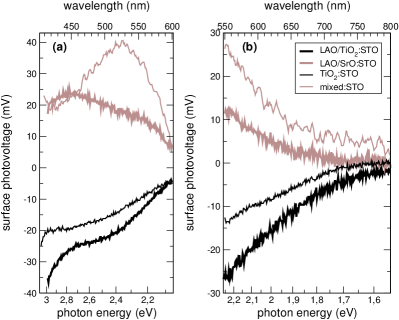
Let us start with a discussion of the general shape of the sub-bandgap444In the following we use the term sub-bandgap with respect to the band gap of SrTiO3 (for LaAlO3 the whole spectral range covered by our light source is sub-bandgap). surface photovoltage spectra, as shown in figure 1. There, the thick lines represent the two LAO/STO heterostructure samples and the thinner lines stand for the bare STO reference samples, respectively.
Considering the LAO/TiO2:STO and the LAO/SrO:STO spectra first, we notice that both spectra are clearly different as they exhibit (i) higher absolute values of the SPV for the sample with the conducting interface, which might be directly linked to the higher interface conductivity, as well as (ii) different signs of the SPV. A detailed microscopic clarification of the origin of the different signs would be too speculative, since this would require a concrete idea of the band lineup at the two different LAO/STO interfaces. To date there exists no consensus regarding the proposed band alignments, the prediction and measurement of the built-in fields, band offsets, band bending, or band discontinuities Cancellieri et al. (2011); Reinle-Schmitt et al. (2012); Chambers (2011); Breitschaft et al. (2010); Qiao et al. (2011); Yoshimatsu et al. (2008); Guduru et al. (2013).
More illuminative is the comparative view on the spectra of the bare STO samples, which serve as a reference. Obviously, the TiO2-terminated STO sample behaves very similar to the LAO/TiO2:STO heterostructure and the STO sample with mixed SrO/TiO2 termination behaves more like the LAO/SrO:STO heterostructure, at least with respect to the sign of the STV. Regarding the fact that it is not a pure SrO termination, this is quite astonishing. Thus, from this rough analysis, it is mainly the STO’s termination, which determines the sub-bandgap SPV response and the related defect state distribution and dynamics.
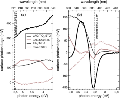
Finding such general shape similarities between the super-bandgap spectra of the four samples, as depicted in figure 2, is not equally possible, since each of the samples shows quite individual spectral features, apart from the STO band gap being visible in all of the spectra. Part of the super-bandgap features might directly originate from higher optical transitions (cf. Yacoby and Naveh, 1973), others may stem from the convolution of the SPV spectrum with multi-level relaxation processes, which are typical for SrTiO3 under super-bandgap excitation Beyreuther et al. (2013, 2011), or persistent photoconductivity effects Tebano et al. (2012).
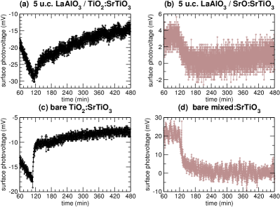
The clear shape similarities that were visible in the sub-bandgap SPV spectra are further evidenced by the light-off SPV transients of the four samples, see figure 3, with the same sample pairs showing similar shapes.
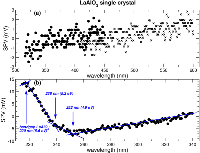
Further, though weaker, evidence for the major role of the STO physics and the minor role of the LAO for the electronic defect state distribution and dynamics, can be derived from the SPV spectra of the bare LAO single crystal, as depicted in figure 4. Between 600 and 300 nm there is almost no SPV response, and from 300 to 220 nm the SPV is much lower than in the STO-based samples.
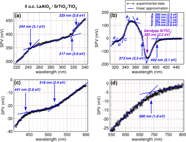
III.2 Spectral features
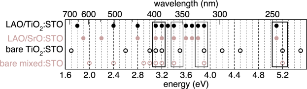
We continue with a more detailed examination of the several spectral features. As described in the introductory part, points of slope changes in sub-bandgap SPV spectra are commonly associated with the energetic positions of electronic defect states located within the band gap. Figure 5 shows the full analysis of the SPV spectra of the LAO/TiO2:STO heterostructure. Points of slope changes are derived from the intersection points of the linear approximations of the parts with constant slope. The corresponding wavelengths and photon energies are given at the respective arrows. The SPV spectra of the LAO/SrO:STO and the two bare STO crystals were analyzed in the same manner. The corresponding figures have been shifted to the supplement (figures S3–S5). For all four samples, the extracted energetic positions of the points of slope change are summarized in figure 6. At least for the sub-bandgap range of STO, i.e. up to 3.2 eV, this graphics represents a map of the in-gap states, which will be discussed in the following:
Within the sub-bandgap range no features common to all four samples were observed. In contrast to the overall shape (see figure 1 again), all four in-gap state distributions are different. Only the feature at 3.1 eV shortly below the STO bandgap, which can be attributed to shallow states and/or a pronounced Franz-Keldysh effect as often observed in SPV spectra, and the feature at 3.2 eV due to band-to-band excitation of carriers are, as expected from our former SPV results on manganite/STO heterostructures Beyreuther et al. (2011) and STO single crystals Beyreuther et al. (2013), present in all samples.
The feature at 2.8 eV (approx. 440 nm) appears only in the two LAO-covered samples and is probably the same level as observed by Wang et al. Wang et al. (2011). There, the level was explained as ”self-trapped exciton state/impurity level” according to former works on STO single crystals Baer (1966); Lee, Destry, and Brebner (1975); Kan et al. (2005). Here, this level might be induced by the LAO deposition process, which possibly modified the STO defect configuration, since none of the bare STO samples shows this feature. In this context it would be highly interesting to study the evolution of this level in gradually more defective samples or in a sample series with growing number of LAO unit-cell layers.
The features at 1.8 eV (LAO/SrO:STO) and 1.9 eV (LAO/ TiO2:STO) probably have the same origin – a deep oxygen vacancy defect level – and were also observed in the optical absorption measurements by Wang et al. Wang et al. (2011), while the third pronounced in-gap state at 2.4 eV below the conduction band reported there is not unambigously visible in our data. Such a level is only present in LAO/TiO2:STO and – astonishingly – in the bare STO with mixed termination.
The discussion of the features above the STO bandgap appears to be more problematic, since already the overall shapes of the spectra are hardly comparable (see again figure 2). Furthermore, the SPV transient behavior of STO under illumination with super-bandgap light is characterized by multiple carrier transfer processes, which take place at long time scales of minutes or even hours Beyreuther et al. (2013). As a consequence, spectral features might interfere with transient features and the SPV spectra can hardly be interpreted as a true energetic map of electronic states. Certainly, higher optical transitions in the STO play a decisive role in this spectral range, while the following point suggests that in-gap states communicating with the LAO bands are of minor importance: If the LAO single crystal is taken as reference (figure 4), two levels at 4.9 eV and 5.2 eV should be observable exclusively in the LAO-covered samples. However, at 4.9 eV no point of slope change was observed, while for 5.1/5.2 eV indeed a level is found – but also for the bare STO crystals, which cannot be exhaustively explained at the current state of knowledge.
IV Summary and outlook
Spectral and time-resolved measurements of the surface photovoltage were employed to compare two 5-u.c.-thick LaAlO3 films on either TiO2- or SrO-terminated SrTiO3 as well as two bare SrTiO3 single crystals with the respective surface terminations with regard to their distribution of electronic interface states. The detailed analysis of the sub-bandgap SPV spectra showed a quite individual defect state map for each of the four samples. However, there were very clear similarities in (i) the sign and the shape of the sub-bandgap spectra as well as (ii) the shape of the light-off SPV transients at 600 nm excitation wavelength between the two TiO2-terminated samples and the two SrO-terminated ones, respectively. This result is in accordance with a number of recent publications, in which the creation of a conducting interface did not necessarily require a crystalline LaAlO3 film Chen et al. (2012); Lee et al. (2012); Delahaye and Grenet (2012); Christensen et al. (2013), but seemed to be crucially dependent on the physics of the SrTiO3 substrate. Still, this remains a key point of the debate, since at the same time there is strong evidence that the LAO stoichiometry plays a decisive role for the creation of the conducting electron liquid Warusawithana et al. (2013).
In order to improve the microscopic picture of the charge dynamics in oxide heterostructures including a less speculative association of the SPV spectral features to bulk- or interface related electronic trap states, the collection of further data, e.g. on LAO/STO samples with gradually changed LAO thickness and with gradually changed oxygen vacancy concentration is indispensable. Such investigations should becarried out in an ultrahigh-vacuum environment to eliminate extrinsic SPV contributions, which typically complicate the shape of the SPV transients Foussekis, Baski, and Reshchikov (2009).
Acknowledgements.
This work was financially supported by the German Research Foundation (BE 3804/2-1 and EN 434/31-1). We thank Claudia Cancellieri, Stefano Gariglio, and Jean-Marc Triscone for providing us with samples and for invaluable discussions.References
- Ohtomo and Hwang (2004) A. Ohtomo and H. Hwang, “A high-mobility electron gas at the LaAlO3/SrTiO3 heterointerface,” Nature 427, 423–426 (2004).
- Maurice et al. (2007) J.-L. Maurice, I. Devos, M.-J. Casanove, C. Carrétéro, G. Gachet, G. Herranz, D.-G. Crété, D. Imhoff, A. Barthélémy, M. Bibes, K. Bouzehouane, C. Deranlot, S. Fusil, E. Jacquet, B. Domengès, and D. Ballutaud, “Charge imbalance at oxide interfaces: How nature deals with it,” Mater. Sci. Eng. B 144, 1–6 (2007).
- Pauli and Willmott (2008) S. A. Pauli and P. R. Willmott, “Conducting interfaces between polar and non-polar insulating perovskites,” J. Phys.: Condens. Matter 20, 264012 (2008).
- Chambers et al. (2011) S. A. Chambers, M. H. Engelhard, V. Shutthanandan, Z. Zhu, T. C. Droubay, L. Qiao, P. V. Sushko, T. Feng, H. D. Lee, T. Gustafsson, E. Garfunkel, A. B. Shah, J.-M. Zuo, and Q. M. Ramasse, “Instability, intermixing and electronic structure at the epitaxial LaAlO3/SrTiO3(001) heterojunction,” Surf. Sci. Rep. 65, 317–352 (2011).
- Zubko et al. (2011) P. Zubko, S. Gariglio, M. Gabay, P. Ghosez, and J.-M. Triscone, “Interface Physics in Complex Oxide Heterostructures,” Annu. Rev. Condens. Matter Phys. 1, 141–165 (2011).
- Reyren et al. (2007) N. Reyren, S. Thiel, A. D. Caviglia, L. F. Kourkoutis, G. Hammerl, C. Richter, C. W. Schneider, T. Kopp, A.-S. Ruetschi, D. Jaccard, M. Gabay, D. A. Muller, J.-M. Triscone, and J. Mannhart, “Superconducting interfaces between insulating oxides,” Science 317, 1196–1199 (2007).
- Caviglia et al. (2008) A. D. Caviglia, S. Gariglio, N. Reyren, D. Jaccard, T. Schneider, M. Gabay, S. Thiel, G. Hammerl, J. Mannhart, and J. M. Triscone, “Electric field control of the LaAlO3/SrTiO3 interface ground state,” Nature 456, 624–627 (2008).
- Brinkman et al. (2007) A. Brinkman, M. Huijben, M. Van Zalk, J. Huijben, U. Zeitler, J. C. Maan, W. G. Van der Wiel, G. Rijnders, D. H. A. Blank, and H. Hilgenkamp, “Magnetic effects at the interface between non-magnetic oxides,” Nat. Mater. 6, 493–496 (2007).
- Cen et al. (2008) C. Cen, S. Thiel, G. Hammerl, C. W. Schneider, K. E. Andersen, C. S. Hellberg, J. Mannhart, and J. Levy, “Nanoscale control of an interfacial metal-insulator transition at room temperature,” Nat. Mater. 7, 298–302 (2008).
- Cen et al. (2009) C. Cen, S. Thiel, J. Mannhart, and J. Levy, “Oxide Nanoelectronics on Demand,” Science 323, 1026–1030 (2009).
- Irvin et al. (2010) P. Irvin, Y. Ma, D. F. Bogorin, C. Cen, C. W. Bark, C. M. Folkman, C.-B. Eom, and J. Levy, “Rewritable nanoscale oxide photodetector,” Nat. Photonics 4, 849–852 (2010).
- Dikin et al. (2011) D. A. Dikin, M. Mehta, C. Bark, C. M. Folkman, C. B. Eom, , and V. Chandrasekhar, “Coexistence of Superconductivity and Ferromagnetism in Two Dimensions,” Phys. Rev. Lett. 107, 056802 (2011).
- Li et al. (2011) L. Li, C. Richter, J. Mannhart, and R. C. Ashoori, “Coexistence of Magnetic Order and Two-dimensional Superconductivity at LaAlO3/SrTiO3 Interfaces,” Nature Phys. 7, 762–766 (2011).
- Cancellieri et al. (2011) C. Cancellieri, D. Fontaine, S. Gariglio, N. Reyren, A. D. Caviglia, A. Fête, S. J. Leake, S. A. Pauli, P. R. Willmott, M. Stengel, P. Ghosez, and J. Triscone, “Electrostriction at the LaAlO3/SrTiO3 Interface,” Phys. Rev. Lett. 107, 056102 (2011).
- Rubano et al. (2011) A. Rubano, M. Fiebig, D. Paparo, A. Marino, D. Maccariello, U. Scotti di Uccio, F. Miletto Granozio, L. Marrucci, C. Richter, S. Thiel, and J. Mannhart, “Spectral and spatial distribution of polarization at the LaAlO3/SrTiO3 interface,” Phys. Rev. B 83, 155405 (2011).
- Ristic et al. (2011) Z. Ristic, R. Di Capula, G. M. De Luca, F. Chiarella, G. Ghiringhelli, J. C. Cezar, N. B. Brookes, C. Richter, J. Mannhart, and M. Salluzzo, “Nanoscale modulation of the density of states at the conducting interface between LaAlO3 and SrTiO3 band insulators,” EPL 93, 17004 (2011).
- Thiel et al. (2006) S. Thiel, G. Hammerl, A. Schmehl, C. W. Schneider, and J. Mannhart, “Tunable Quasi-Two-Dimensional Electron Gases in Oxide Heterostructures,” Science 313, 1942–1945 (2006).
- Pauli et al. (2011) S. A. Pauli, S. J. Leake, B. Delley, M. Björck, C. W. Schneider, C. M. Schlepütz, D. Martoccia, S. Paetel, J. Mannhart, and P. R. Willmott, “Evolution of the Interfacial Structure of on ,” Phys. Rev. Lett. 106, 036101 (2011).
- Reinle-Schmitt et al. (2012) M. L. Reinle-Schmitt, C. Cancellieri, D. Li, D. Fontaine, M. Medarde, E. Pomjakushina, C. W. Schneider, S. Gariglio, P. Ghosez, J.-M. Triscone, and P. R. Willmott, “Tunable conductivity threshold at polar oxide interfaces,” Nature Comm. 3, 932 (2012).
- Liu et al. (2013) Z. Q. Liu, C. J. Li, W. M. Lü, X. H. Huang, Z. Huang, S. W. Zeng, X. P. Qiu, L. S. Huang, A. Annadi, J. S. Chen, J. M. D. Coey, T. Venkatesan, and Ariando, “Origin of the Two-Dimensional Electron Gas at Interfaces: The Role of Oxygen Vacancies and Electronic Reconstruction,” Phys. Rev. X 3, 021010 (2013).
- Chambers (2011) S. A. Chambers, “Understanding the mechanism of conductivity at the LaAlO3/SrTiO3(001) interface,” Surf. Sci. 605, 1133–1140 (2011).
- Rubano et al. (2013) A. Rubano, T. Günter, T. Fink, D. Paparo, L. Marrucci, C. Cancellieri, S. Gariglio, J.-M. Triscone, and M. Fiebig, “Influence of atomic termination on the LaAlO3/SrTiO3 interfacial polar rearrangement,” Phys. Rev. B 88, 035405 (2013).
- Breitschaft et al. (2010) M. Breitschaft, V. Tinkl, N. Pavlenko, S. Paetel, C. Richter, J. R. Kirtley, Y. C. Liao, G. Hammerl, V. Eyert, T. Kopp, and J. Mannhart, “Two-dimensional electron liquid state at LaAlO3-SrTiO3 interfaces,” Phys. Rev. B 81, 153414 (2010).
- Ristic et al. (2012) Z. Ristic, R. Di Capua, F. Chiarella, G. M. De Luca, I. Maggio-Aprile, M. Radovic, and M. Saluzzo, “Photodoping and in-gap interface states across the metal-insulator transition in LaAlO3/SrTiO3 heterostructures,” Phys. Rev. B 86, 045127 (2012).
- Drera et al. (2011) G. Drera, F. Banfi, F. F. Canova, P. Borghetti, L. Sangaletti, F. Bondino, E. Magnano, J. Huijben, M. Huijben, G. Rijnders, D. H. A. Blank, H. Hilgenkamp, and A. Brinkman, “Spectroscopic evidence of in-gap states at the SrTiO3/LaAlO3 ultrathin interfaces,” Appl. Phys. Lett. 98, 052907 (2011).
- Koitzsch et al. (2011) A. Koitzsch, J. Ocker, M. Knupfer, M. C. Dekker, K. Dörr, B. Büchner, and P. Hoffmann, “In-gap electronic structure of LaAlO3-SrTiO3 heterointerfaces investigated by soft x-ray spectroscopy,” Phys. Rev. B 84, 245121 (2011).
- Cancellieri et al. (2013) C. Cancellieri, M. L. Reinle-Schmitt, M. Kobayashi, V. N. Strocov, T. Schmitt, P. R. Willmott, S. Gariglio, and J. Triscone, “Interface Fermi States of LaAlO3/SrTiO3 and Related Heterostructures,” Phys. Rev. Lett. 110, 137601 (2013).
- Wang et al. (2011) X. Wang, J. Q. Chen, A. Roy Barman, S. Dhar, Q.-H. Xu, T. Venkatesan, and Ariando, “Static and ultrafast dynamics of defects of SrTiO3 in LaAlO3/SrTiO3 heterostructures,” Appl. Phys. Lett. 98, 081916 (2011).
- Johnson (1958) E. Johnson, “Large-Signal Surface Photovoltage Studies with Germanium,” Phys. Rev. 111, 153–166 (1958).
- Lagowski et al. (1992) J. Lagowski, P. Edelman, M. Dexter, and W. Henley, “Non-contact mapping of heavy metal contamination for silicon ic fabrication,” Semicond. Sci. Technol. 7, A182–A192 (1992).
- Schroder (2006) D. K. Schroder, Semiconductor Material and Device Characterization, 3rd ed. (John Wiley & Sons, 2006).
- Gatos and Lagowski (1973) H. C. Gatos and J. Lagowski, “Surface Photovoltage Spectroscopy - A New Approach to the Study of High-Gap Semiconductor Surfaces,” J. Vac. Sci. Technol. 10, 130–135 (1973).
- Lagowski (1994) J. Lagowski, “Semiconductor surface spectroscopies: the early years,” Surf. Sci. 299/300, 92–101 (1994).
- Kronik and Shapira (1999) L. Kronik and Y. Shapira, “Surface photovoltage phenomena: theory, experiment, and applications,” Surf. Sci. Rep. 37, 1–206 (1999).
- Kronik and Shapira (2001) L. Kronik and Y. Shapira, “Surface photovoltage spectroscopy of semiconductor structures: at the crossroads of physics, chemistry and electrical engineering,” Surf. Interface Anal. 31, 954–965 (2001).
- Duzhko et al. (2001) V. Duzhko, V. Y. Timoshenko, F. Koch, and T. Dittrich, “Photovoltage in nanocrystalline porous TiO2,” Phys. Rev. B 64, 075204 (2001).
- Li, Jia, and Li (2002) L. S. Li, Q. X. Jia, and A. D. Q. Li, “Effects of Organic Self-assembled Polymer and Metal Phtalocyanine Multilayers on the Surface Photovoltaic Properties of Indium Tin Oxide and Titanium Oxide,” Chem. Mater. 14, 1159–1165 (2002).
- Mavroides and Kolesar (1978) J. G. Mavroides and D. F. Kolesar, “Surface photovoltage experiments on SrTiO3 electrodes,” J. Vac. Sci. Technol. 15, 538–541 (1978).
- Beyreuther et al. (2013) E. Beyreuther, J. Becherer, A. Thiessen, S. Grafström, and L. M. Eng, “Electronic surface properties of SrTiO3 derived from a surface photovoltage study,” Surf. Sci. 612, 1–9 (2013).
- Beyreuther et al. (2011) E. Beyreuther, A. Thiessen, J. Becherer, S. Grafström, K. Dörr, and L. M. Eng, “Probing electronic defect states in manganite/SrTiO3 heterostructures by surface photovoltage spectroscopy,” Mat. Sci. Engin. B 176, 446–452 (2011).
- Note (1) Of course, a LAO bulk crystal cannot act as a real reference for a 5-u.c.-thick thin film, since its physical properties might be decisively different. On the other hand it is not possible to check the SPV behavior of a free-standing film. Thus the usage of the bulk crystal is a compromise, also because there is no SPV data on LAO available in literature so far.
- Koster et al. (1998) G. Koster, B. L. Kropman, G. Rijnders, D. H. A. Blank, and H. Rogalla, “Quasi-ideal strontium titanate crystal surfaces through formation of strontium hydroxide,” Appl. Phys. Lett. 73, 2920–2922 (1998).
- Note (2) Using two different photon fluxes was motivated as follows: The photon flux is limited by the output power of the Xe arc lamp. The latter drops dramatically in the ultraviolet range. Thus, the maximum achievable flux at 220 nm determines the flux for the whole spectrum. On the other hand, at the other end of the spectral range, on the long-wavelength side – far away from the STO and LAO bandgaps – the SPV response is quite low. Thus we decided to use a slightly higher photon flux for the two long-wavelength spectra.
- Note (3) See supplemental material at http://www.iapp.de/~elke/preprints/Beyreuther_et_al_2013_LAO_STO_SPV_supplement.pdf for additional diagramms of the SPV data.
- Note (4) In the following we use the term sub-bandgap with respect to the band gap of SrTiO3 (for LaAlO3 the whole spectral range covered by our light source is sub-bandgap).
- Qiao et al. (2011) L. Qiao, T. C. Droubay, T. C. Kaspar, P. V. Sushko, and S. A. Chambers, “Cation mixing, band offsets and electric fields at LaAlO3/SrTiO3(001) heterojunctions with variable La:Al atom ratio,” Surf. Sci. 605, 1381–1387 (2011).
- Yoshimatsu et al. (2008) K. Yoshimatsu, R. Yasuhara, H. Kumigashira, and M. Oshima, “Origin of Metallic States at the Heterointerface between the Band Insulators LaAlO3 and SrTiO3,” Phys. Rev. Lett. 101, 026802 (2008).
- Guduru et al. (2013) V. K. Guduru, A. Granados del Aguila, S. Wenderich, M. K. Kruize, A. McCollam, P. C. M. Christianen, U. Zeitler, A. Brinkman, G. Rijnders, H. Hilgenkamp, and J. C. Maan, “Optically excited multi-band conduction in LaAlO3/SrTiO3 heterostructures,” Appl. Phys. Lett. 102, 051604 (2013).
- Yacoby and Naveh (1973) Y. Yacoby and O. Naveh, “Differential optical spectra and band structure of SrTiO3,” Phys. Rev. B 7, 3991–4000 (1973).
- Tebano et al. (2012) A. Tebano, E. Fabbri, D. Pergolesi, G. Balestrino, and E. Traversa, “Room-Temperature Giant Persistent Photoconductivity in SrTiO3/LaAlO3 Heterostructures,” ACS Nano 2, 1278–1283 (2012).
- Baer (1966) W. Baer, “Free-Carrier Absorption in Reduced SrTiO3,” Phys. Rev. 144, 734–738 (1966).
- Lee, Destry, and Brebner (1975) C. Lee, J. Destry, and J. Brebner, “Optical absorption and transport in semiconducting SrTiO3,” Phys. Rev. B 11, 2299–2310 (1975).
- Kan et al. (2005) D. Kan, T. Terashima, R. Kanda, A. Masuno, K. Tanaka, S. Chu, H. Kan, A. Ishizumi, Y. Kanmitsu, Y. Shimakawa, and M. Takano, “Blue-light emission at room temperature from Ar+-irradiated SrTiO3,” Nature Materials 4, 816–819 (2005).
- Chen et al. (2012) Y. Z. Chen, D. V. Christensen, F. Trier, N. Pryds, A. Smith, and S. Linderoth, “On the origin of metallic conductivity at the interface of LaAlO3/SrTiO3,” Appl. Surf. Sci. 258, 9242–9245 (2012).
- Lee et al. (2012) S. W. Lee, Y. Liu, J. Heo, and R. G. Gordon, “Creation and Control of Two-Dimensional Electron Gas Using Al-Based Amorphous Oxides/SrTiO3 Heterostructures Grown by Atomic Layer Deposition,” Nano Lett. 12, 4775–4783 (2012).
- Delahaye and Grenet (2012) J. Delahaye and T. Grenet, “Metallicity of the SrTiO3 surface induced by room temperature evaporation of alumina,” J. Phys. D: Appl. Phys. 45, 315301 (2012).
- Christensen et al. (2013) D. V. Christensen, F. Trier, Y. Z. Chen, A. Smith, J. Nygård, and N. Pryds, “Controlling interfacial states in amorphous/crystalline LaAlO3/SrTiO3 heterostructures by electric fields,” Appl. Phys. Lett. 102, 021602 (2013).
- Warusawithana et al. (2013) M. P. Warusawithana, C. Richter, J. A. Mundy, P. Roy, J. Ludwig, S. Paetel, T. Heeg, A. A. Pawlicki, L. F. Kourkoutis, M. Zheng, M. Lee, B. Mulcahy, W. Zander, Y. Zhu, J. Schubert, J. N. Eckstein, D. A. Muller, C. Stephen Hellberg, J. Mannhart, and D. G. Schlom, “LaAlO3 stoichiometry found key to electron liquid formation at LaAlO3/SrTiO3 interfaces,” arXiv:1303.5352 [cond-mat.mtrl-sci] (2013).
- Foussekis, Baski, and Reshchikov (2009) M. Foussekis, A. A. Baski, and M. A. Reshchikov, “Photoadsorption and photodesorption for GaN,” Appl. Phys. Lett. 94, 162116 (2009).