Origin of two-dimensional electron gases at oxide interfaces: insights from theory
Abstract
The response of oxide thin films to polar discontinuities at interfaces and surfaces has generated an enormous activity due to the variety of interesting effects it gives rise to. A case in point is the discovery of the electron gas at the interface between LaAlO3 and SrTiO3, which has since been shown to be quasi-two-dimensional, switchable, magnetic and/or superconducting. Despite these findings, the origin of the two-dimensional electron gas is highly debated and several possible mechanisms remain. Here we review the main proposed mechanisms and attempt to model expected effects in a quantitative way with the ambition of better constraining what effects can/cannot explain the observed phenomenology. We do it in the framework of a phenomenological model for understanding electronic and/or redox screening of the chemical charge in oxide heterostructures. We also discuss the effect of intermixing, both conserving and non-conserving the total stoichiometry.
type:
Topical Review1 Introduction
Oxide interfaces have received considerable attention within the past couple decades. From the device perspective, many technological applications depend crucially on interfacial properties and the fundamental understanding at the microscopic level is often critical for optimising device performance. In particular oxide interfaces have also offered the opportunity to discover and study completely novel, and often unexpected, fundamental materials physics. The LaAlO3-SrTiO3 (LAO-STO) interface has become a prototypical example of such a system. In bulk form both oxides are electronically fairly simple non-magnetic insulators. Remarkably, the interface between the two can exhibit metallic [1], magnetic [2] and/or superconducting [3, 4, 5] behaviour of a quasi-two-dimensional character [6]. It has since been proposed that the LAO-STO system may find applications in field effect devices [7, 8], sensors [9], nano-photodetectors [10], thermoelectrics [11, 12], and solar cells [13, 14]. The combination of exotic physical properties and wide-range of potential device applications has made the LAO-STO interface a highly popular system of study with several dedicated reviews and perspectives [15, 16, 17, 18, 19, 20, 21, 22, 23, 24].
Despite the enormous amount of activity on this system, the origin of a two-dimensional electron gas (2DEG) at the LAO-STO interface remains unclear. Arguably the most popular explanation, called the ‘electronic reconstruction’, is based on the concept of a ‘polar catastrophe’ [25]. The concept uses basic electrostatics (see section 2.7) to show that a net charge at a polar, insulating interface such as LAO-STO produces a finite non-decaying electric field. This diverging electrostatic potential is clearly energetically unstable upon increasing thickness of the oxide film. In reality the system requires some form of charge compensation. This might occur through an electronic reconstruction (see section 3) whereby the electric field produces an electronic transfer similar to Zener tunnelling from the surface valence band to the interface conduction band. This process should not be taken too literally. The kinetic process of establishing the 2DEG can be more involved and is beyond the scope of this paper. The polar catastrophe and electronic reconstruction concepts establish the paradigm in an intuitive way. It is interesting, however, that the same mechanism can be seen from a different perspective [26]. There it was noted that the isolated neutral interface and surface should have free carriers associated to them to start with, which (partly) annihilate when brought close to each other. It is an alternative view of the same mechanism, with the same predictions for the equilibrium result, but different perspective on the process.
Alternative explanations suggest that charge compensation may be achieved through chemical modifications or chemical plus electronic (redox) modifications (see section 4). A third category of proposed mechanisms is not based on polarity arguments but instead extrinsic effects induced by the film growth process such as doping through oxygen vacancies or interface cation intermixing (see section 5). Clearly the origin of the 2DEG is not just of academic interest, but key to understand what other systems might show similar behaviour and how one might be able to tune device properties.
A large number of experimental and theoretical studies have been devoted to clarify which mechanism(s) operates in LAO-STO. A recent short review attempted to summarise the results, concluding that the electronic reconstruction mechanism appears to support experiment [21]. The electronic reconstruction mechanism is certainly strongly supported by several experimental observations, most notably the observation of a critical thickness of the LAO film for the onset of interface conductivity [7] which can be tuned [27]. However the electronic reconstruction mechanism does not naturally explain all experimental observations. For example the discovery of a sizeable density of (trapped) Ti 3 like states below the critical thickness [28, 29, 30, 31, 32], the lack of surface hole carriers [7] or states near the Fermi level [33, 34], the almost negligible electric field within LAO below the critical thickness [35, 32, 36], and the apparent disappearance of conductivity at any LAO thickness for samples grown at high Oxygen partial pressures [37, 38]. It is apparent that the situation is not so clear.
The main aim here is to review the findings for this and related systems in the framework of a simple model. This model describes simply but quantitatively the several effects that concur in the physics of such systems. In doing so, we hope to better constrain what effects can/cannot explain the observed phenomenology. It is therefore limited in scope and far from any ambition of being exhaustive in the review of the activity around these systems. In section 2 we briefly introduce the concept of polar interfaces, highlighting for the case of LAO-STO the basic theory behind determining the interface net charge and resulting electrostatics. We then begin by exploring the various proposed mechanisms behind the origin of 2DEGs at oxide interfaces. We present a phenomenological model for understanding electronic and/or redox screening of the chemical charge in polar heterostructures in sections 3 and 4. In section 5 we discuss the effect of intermixing, both conserving and non-conserving the total stoichiometry.
2 Polar interfaces
2.1 The net charge
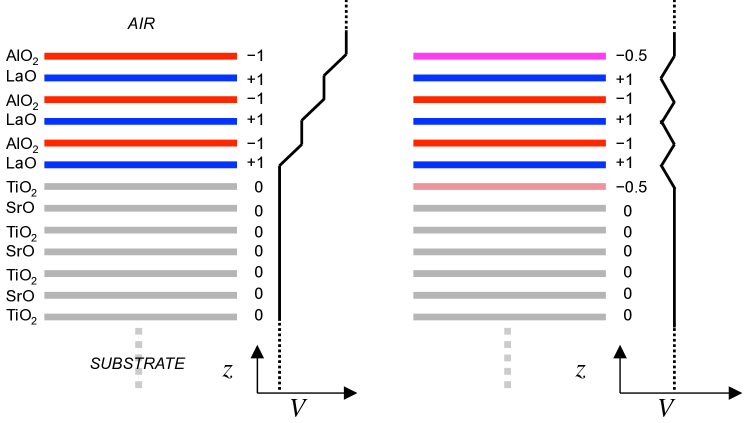
In the seminal paper of Ohtomo and Hwang [1] the discovery of the two-dimensional electron gas at the interface between the two nominally insulating oxides, LAO and STO, was rationalised in terms of the electrostatics of the formal charges on each ion, i.e. -2 for O, +4 for Ti and so on, as illustrated in Fig. 1. From these formal charges, the (001) layers in STO (SrO and TiO2) are charge neutral whilst in LAO (LaO and AlO2) they are +1 and -1 per layer formula unit. At the (001) LAO-STO interface, taking the two unperturbed bulk materials 111The polarisation response and electronic and redox screening of polar interfaces will be discussed in sections 2.7, 3 and 4, respectively., these layer charges give rise to an imbalance at the interface of 0.5 . The sign depends on the interface termination, and is the 2D interface unit cell area corresponding to one formula unit. These basic arguments, built upon the formal ionic charges, are at the heart of almost all subsequent work on this system.
It is tempting to suggest a renormalisation of these numbers by introducing covalency factors in an attempt to correct for realistic bonding in these far from ideally ionic O3 materials. It is well known that in most perovskites there is a sizeable covalent bonding character, especially in the -O bonds. One would then find after repeating the basic procedure above an arbitrary value of the interface charge smaller than 0.5 .
The first point we wish to highlight here is that when determining the net interface charge in these materials it would be incorrect to include covalency considerations such as that just mentioned (see ref. [39] for further discussion). The net interface charge of these band insulators is exactly as obtained from the simple counting of the formal charges on each species irrespective of covalency 222In crystals lacking a symmetry forbidding local dipoles on the atoms, the formal ionic charges are not sufficient for determining the surface/interface charge [40]. In such cases the polarisation analysis explained in section 2.2 using the modern theory of polarisation would be correct, while an analysis based on formal charges alone would not.. For LAO-STO, the net interface charge is precisely 0.5 [41, 42].
Let us discuss this further. We outline the arguments proposed in refs. [42, 43, 41, 39, 40]. For electrostatics purposes (see next section) the calculation of the resulting electric field from an interface requires the knowledge of both the area density of free charges and the total polarisation, or bound charges (including the electric field response - see next section) of each material. The subtlety of the problem comes from what is meant by free charges and the definition of the polarisation. Remember we are considering the unperturbed bulk interface, so zero free charges in a strict sense. However the free charge can also be defined as anything unaccounted for by the polarisation, and previously called chemical [41] or compositional charge [44]. The key to the problem is in the definition of the reference unperturbed (zero of) polarisation: altering its value will change the free charge by the same amount. In the end it is the sum of the two that matters and is unaffected. Centrosymmetric materials such as LAO and STO allow for a natural definition of zero polarisation, the effective polarisation then being the change of polarisation after some perturbation from the centrosymmetric reference. Taking the polarisation of STO and LAO as zero, one can then use a charge counting technique such as the ’polarisation-free’ unit cell method [45] to find a free (or chemical/compositional) interface charge density of 0.5 .
2.2 Polarisation and quanta
An alternative viewpoint, that is perhaps more elegant and rigorous, has been proposed [42] which considers the formal polarisation instead of the effective value above. The formal polarisation is obtained by direct application of the modern theory of polarisation [46], for example by taking the ionic cores and charge centre of Wannier functions [47] as point charges. The difference between the two definitions, effective and formal, for the case of LAO-STO is exactly 0.5 : whilst the effective value for LAO and STO is zero, the formal values are 0.5 and zero, respectively. Within this definition the free charges are now zero, but the sum of free and bound charges remains 0.5 and hence the resulting electrostatic analysis is unaltered.
We have neglected to mention so far one more subtlety. In a system of discrete point charges the bulk polarisation is defined only up to quanta of polarisation. When the definition of the bulk unit cell is displaced along a crystallographic direction and reaches one of the point charges, it disappears there and reappears at the other side of the unit cell. At this point the obtained polarisation jumps by a finite value of
which is called a quantum of polarisation, where is the length of the cell along the direction of the flip, and is the cell volume (polarisation as dipole per unit volume). Clearly there is no a priori best choice of the unit cell as long as the surface is unknown. The bulk polarisation value is therefore only defined modulo polarisation quanta. In centrosymmetric perovskites two sets of formal polarisation values are allowed,
as in STO, and
as in LAO, since these are the only two sets that are invariant under change of sign. This is the key difference with the effective polarisation as defined above, where all centrosymmetric materials were defined to have 0 polarisation: now they can have 0 or , both modulo .
2.3 Symmetry and topology
We have approached the problem of determining the polarisation from a perspective based on point charges using the centre of charge of the valence band Wannier functions [47]. An alternative approach defines the bulk polarisation of an insulator in terms of a Berry phase [46, 49]. This formulation, called the modern theory of polarisation, arises from the consideration of the current that flows through the system when adiabatically changing its polarisation state. In 1984 it was established by Berry [50] that such an adiabatic change of a Hamiltonian is associated with the appearance of a complex phase in the wave-function that describes the system as it adiabatically evolves. This phase is of deep physical significance and is called a geometric phase, which, in principle can take any value, corresponding to an arbitrary value of the polarisation. The presence of a symmetry pins the polarisation (and corresponding phase) to particular values, and the phase is referred to as topological.
In centrosymmetric insulators like LAO and STO, the two possible values of the polarisation 0 and (both modulo ) described in section 2.2 correspond to the two values of the Berry phase, 0 and , modulo . It is interesting to make the analogy with other symmetry-protected topological phases (in e.g. topological insulators). Here the relevant symmetry is e.g. time-reversal, and the topological phase relates to other properties, e.g. to magnetisation or its susceptibility. In the conventional table for topological insulators, one axis corresponds to the relevant symmetry, its entries conventionally being time reversal, particle-hole and their product. Arguably, in this table categorising the different symmetry-protected topological phases, spatial symmetries should also feature, which would then include the insulators considered in this review. It has already been done for two-dimensional systems [51, 52], referring to the quantisation of electric polarisation, as discussed here. Interestingly, for other symmetry groups, as for honeycomb planar insulators (e.g. BN), there are more than two sets of consistent values, three in this case [51]. (There are further topological classifications of insulators based on crystal symmetries, but in a different context to the one of this review [53].) In analogy with other topological insulators, the interface between two insulators of different topological character in this sense, as LAO and STO, gives rise to a 2DEG. Of course, such 2DEGs are not topologically protected against any kind of defect breaking the symmetry defining the phase. This is analogous to the situation relating to a topological insulator: the 2DEG arising on its surface is not protected against defects breaking the time-reversal symmetry, such as magnetic impurities. In this case, the 2DEG is affected by regular disorder and defects.
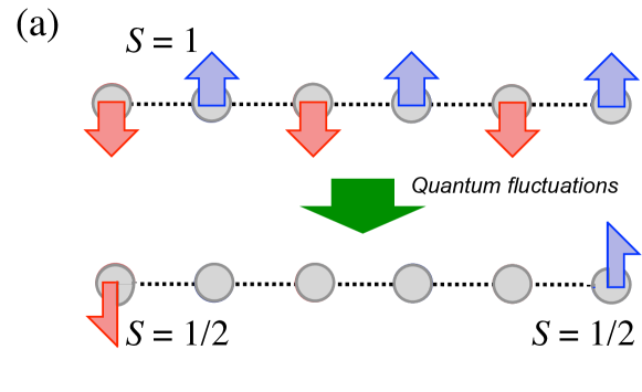
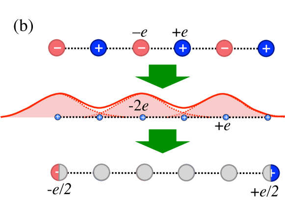
The analogy with other symmetry protected topological phases is best illustrated referring to a “perspective article” of X. Qi in Science in 2012 [48]. Here the concept of a symmetry-protected topological phase is transmitted in terms of the Haldane chain, a one-dimensional Heisenberg model of localised quantum spins with S=1, interacting antiferromagnetically. In the ground state for a finite chain, the quantum fluctuations of the local spins act in such a way that the chain appears as if without spins, except for a net spin of at one end and at the other, in spite of their being no particles anywhere in the system.
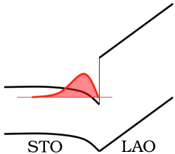
That system is beautifully analogous to a chain of alternating charges, and some quantum of charge, which is again analogous to the (100) atomic planes of LAO (see Figure 1 of ref. [39]). The net effect is that of half a quantum of charge of either sign at either end, as sketched in Fig. 2 (the quantum fluctuations in this case manifest themselves on the delocalisation illustrated in the figure for the electrons).
2.4 Other interface planes
The discussion above was centred around the heterostructures grown in (001) planes because most experiments have been performed for those systems, in addition to the simplicity they offer. The generalisation to other growth directions is simple, both using formal charges or using polarisation. Using formal charges, the argument goes parallel to the original one by Ohtomo and Hwang [1]. The stacking of [001] atomic layers in the ABO3 perovskite is AO/BO2/AO/BO2, and thus with formal charges , , , , for LAO, while they are all neutral for STO. Similarly the stacking of [111] layers is AO3/B/AO3/B, and therefore with alternating and charges in LAO, and and for STO. For [011] the stacking is ABO/O2/ABO/O2, and the resulting formal charges are and for both materials. One would thus expect a polarisation discontinuity in [001] and [111] but not in [011].
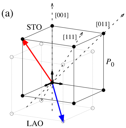

Going back to the polarisation discussion, the arguments above generalise to 3D from the 1D set proposed in such a way that for one meaningful value of the polarisation there is a whole 3D lattice of values. In the STO case, and assuming the cubic phase for simplicity, the lattice is simple cubic, with as lattice parameter, and such that is a member of the set. For LAO the lattice is also simple cubic, but now the origin is at the centre of a cube, and thus not part of the set. This is illustrated in Fig. 3 (a), and it is analogous to the polarisation lattices already presented in the pioneering paper of Vanderbilt and King-Smith [43], and to the recent proposal for 2D honeycomb (graphenic) insulators in ref. [51].
In order to predict for possible polarisation discontinuities of these two materials in interfaces of arbitrary orientation, one selects the direction normal to the interface and projects all vectors of the lattice for each material onto the particular direction line. This is illustrated in Fig. 3, using the [001], [011] and [111] directions as examples. The projections proposed in Fig. 3 (a) give rise to the 1D sets for the three directions, shown in Fig. 3 (b), for both the STO (continuum lines and filled circles) and the LAO case (dotted lines and open circles). It is very apparent that both for (001) and (111) interfaces there are no possible choices of for both materials such that ; there is always a discontinuity in the polarisation.
Consistently with this discussion and in addition to the well-known 2DEG in the (001) case, a 2DEG has been recently discovered at the (111) LAO-STO interface [54]. In this case, the atomic layers are alternating O3 planes and planes, which for LAO means -3 and +3 layers, while in STO it means -4 and +4 layers. There is therefore a discontinuity at the interface corresponding to 0.5 . Noting that (for the as defined in section 2.1, for the (001) case) we see that the formal charges argument, giving a chemical charge of 0.5 , agrees with what obtained from Figure 3, namely, .
While a discontinuity in the polarisation exists for (001) and (111) interfaces, it is not the case for the (011) interface for which interfaces with no discontinuity can be built. This agrees with the consideration from formal charges for which (011) planes of LAO (STO) are made of LaAlO (SrTiO) planes alternating with O2 planes, i.e. alternating planes of and , in both cases. Therefore, as long as a O2 plane always separates O planes, there should be no polarisation discontinuity.
It is interesting, however, that experiments for (011) interfaces [54, 55] show interface conduction similar to what found in the (001) case, in spite of the fact that according to the discussion in the previous paragraph there should be no polar discontinuity at the pristine interface, and thus no intrinsic tendency to accumulate free carriers at the interface. The same study [55] arrives at an explanation of the effect by a careful structural study of the interface, which shows that it is not an ideal epitaxial (011) interface, but rather a heavily stepped one, in a jigsaw pattern of (001) steps and terraces. These do present the polar discontinuity discussed above, thereby explaining the appearance of the 2DEG. This raises the next question, as to why does this pattern emerge at all if the ideal interface would represent no electrostatic penalty whatsoever. The answer as suggested in refs. [56, 55] is likely to be related to the fact that although the ready-made interface would not be polar, the preformed ideal (011) surface of STO is highly so and requires pre-screening, such as the observed formation of the (001) steps and terraces, before the growth of the film.
Finally, the vector lattice above can also be used to predict the polar discontinuities at stepped or vicinal surfaces, as demonstrated in [57]. The direction normal to the average interface defines the global polar discontinuity, although if the interface is constituted by well-defined steps separated by wide terraces, the contribution of steps and terraces can be distinguished, allowing for the preparation of one-dimensional electron gases along the steps [57].
2.5 Removing the arbitrariness
In as much as we are defining the polar discontinuity at an interface from the bulk polarisation values, there is the indetermination in the lattice of quanta described above. However, the formal polarisation can be argued to give a more defined information for a given surface or interface, even an absolute value, as was already proposed by Vanderbilt and King-Smith [43].
A compelling piece of evidence in this direction is given by the case of the (001) interface between e.g. KTaO3 (KTO) and LaAlO3. Taking the formal charges of -2 for O, +1 for K and +5 for Ta the (001) layers in KTO are +1 (TaO2) and -1 (KO) per layer formula unit. Both LAO and KTO are of the kind, and thus one can foresee a non-polar interface. Yet, an ideal epitaxial interface, if considering formal charges, would show two layers or two layers together at the interface, since the O planes are for LAO, but for KTO, and vice-versa for the O2 planes. Such interfaces would give a net chemical charge of , i.e. . In other words, although an interface between KTO and LAO could be made without polar discontinuity, it seems the ideal epitaxial one is polar. Enhanced carrier densities in interfaces between III-III and I-V perovskites have indeed been predicted in ref. [58].
The fact is that when defining a whole system with explicit surfaces, the absolute polarisation is well defined, and can be measured, as the total dipole over the volume of the sample. The surface theorem essentially says that for specific surface terminations (and as long as the system remains insulating) the total polarisation obtained from the Wannier charge centres gives the absolute value of the polarisation. The absolute value of the polarisation is one specific vector from within the lattice discussed in sections 2.2 and 2.4. This is true as long as the periodicity parallel to each surface is respected. This should be understood in a strict sense: if any local source of charge (ion) is added or removed from the surface, it is done periodically, and therefore respecting charge quantisation per unit cell. This also holds for interfaces. In the KTO/LAO example, the (001) epitaxial interface, i.e., the one respecting the O-O2 plane alternation, gives a polar discontinuity of one whole quantum of polarisation. However if we were to grow an interface in which the first O2 plane of KTO, that is, the TaO2 plane, would grow on a O2 plane of LAO (the AlO2 plane), there would be no polar discontinuity. That is, the termination defines the point in the polarisation set.
2.6 Alternative formulations
Polar surfaces and interfaces have been known for many decades. The description we have reviewed so far started in a seminal paper [43] and is linked to the modern theory of polarisation [46] but there were previous characterisations of such systems. The review of Goniakowski, Finocchi and Noguera [45] gives an excellent account of the varied descriptions of polar surfaces and interfaces. For classical point particles one finds these concepts discussed for related situations in the book by Born and Huang [59]. Tasker, in 1979, offered a characterisation and classification of ideally ionic surfaces [60]. The link between Tasker’s characterisation and the ideas based on the modern theory of polarisation was recently established by Stengel [40].
The treatment for quantum delocalised electrons presents difficulties for some theoretical frameworks, however, related to the problem of how to assign a static charge to the different atoms in a solid. This is the case for instance of the electron counting models of, e.g., Harrison and coworkers [61] by which excess charges were assigned to the cations and anions of heteropolar semiconductors, trying to account for covalency effects. Such techniques were quite successful at a qualitative level when used in conjunction with empirical studies of the electronic structure of materials. The quantitative determination (both from first principles and experimentally) of such quantities however is more problematic, since it involves the assignment of charge to the atoms in the solid, a badly posed problem. It was attacked with different schemes defining atomic charges, probably the most popular one in recent times being the one by Bader [62]. For a brief discussion of the ill-definition of static charge schemes in the context of perovskites we refer the reader to ref. [63].
Interestingly, in highly symmetric systems, like cubic LAO and STO, such charge redistribution terms cancel and the final result for the polar discontinuity coincides with the value established above. For systems in which polarisation is not defined by symmetry, it is by no means obvious to us that the calculation of the polarisation discontinuity by means of such charge attributions should agree with the results obtained from the calculation of the formal polarisation. We will not discuss them further here, and we refer the reader to the aforementioned review for a quite comprehensive discussion of such methods [45].
Finally, another take on the matter worth mentioning is the one due to Finnis [64] who discusses polar surfaces and interfaces in terms of the theory of thermodynamic excesses, a way of thermodynamically considering relative proportions of the different components in a phase when close to a surface, interface or grain boundary. Such excesses (changes of concentration with respect to the bulk phase) also relate to charge excess, which connects with the chemical or compositional charge discussed in section 2.1.
2.7 Electrostatics
Within the macroscopic electrostatics relevant for length scales larger than atomic size, electric fields and charges are related through Gauss’s law, , where is the electric displacement field, and is the charge density of free carriers. For an interface it becomes,
| (1) |
where is the area density of free charges associated to the interface, is taken as the direction normal to the interface and and indicate the materials on either side of the interface. From the definition of the electric displacement field, where is the dielectric permittivity of vacuum, the electric field and the polarisation, we obtain the change in electric field across the interface,
| (2) |
or
| (3) |
Therefore, as stated in section 2.1, for electrostatic purposes it is only the sum of the interface charge and the polarisation discontinuity across the interface that is required to obtain the resultant electric fields. Separating the spontaneous component from the electric field response component of the polarisation, we write
| (4) |
and, as argued above for LAO-STO,
| (5) |
irrespective of whether we use the effective or formal polarisation to define the problem, which from now on we denote by .
The only thing that remains is to define the geometry and electrostatic boundary conditions and to solve for the electric fields self-consistently including the dielectric responses. The most widely studied LAO-STO geometry is a single thin film of LAO of thickness on a TiO2 terminated STO substrate 333For the analogous discussion for a superlattice geometry see ref. [41].. This amounts to a system of two interfaces with equal and opposite charges, similar to the electrostatics of a capacitor. Assuming open-circuit boundary conditions ( within the substrate and vacuum), and taking a linear dielectric response for LAO,
| (6) |
we obtain the usual capacitor expression
| (7) |
where
| (8) |
In other words, in absence of electronic or ionic reconstructions, a constant non-decaying electric field exists in LAO due to the polar interface charge , which is partly screened by the dielectric response of LAO. This dielectric response of LAO in these films has been predicted within first principles calculations [65, 66, 67], and experimentally inferred through surface x-ray diffraction (SXRD) measurements [68] and high-angle annular dark-field imaging (HAADF) [69] which revealed an off-centring of the cation positions along with respect to the ideal perovskite structure, and through the electrostriction effect [70].
3 Electronic reconstruction
3.1 Concept and model
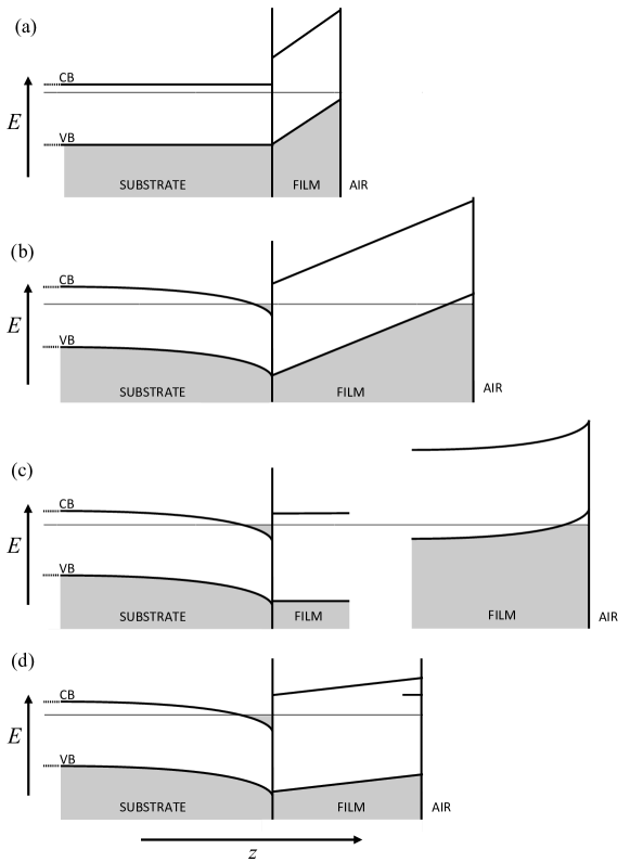
We start with a simple model that describes the “electronic reconstruction” that has been proposed as a mechanism to counter the electrostatic build up that originates when growing a thin film of LaAlO3 on a SrTiO3 substrate (LAO on STO) along the [001] direction [25]. The model captures the essential physics of the pristine system as confirmed by several first principles calculations (see for example refs. [8, 65, 72, 67, 41]). It is illustrated in Figs. 4 (a) and (b): the 0.5 of chemical or compositional charge at the interface and surface (corresponding to the half a quantum of formal polarisation of LAO, see section 2.1 and Ref. [39]) gives rise to an electric field in the film (see section 2.7). This induces a transfer of electrons from the valence band at the surface, to the conduction band at the interface (see Fig. 4 b). The electron transfer only happens once the potential drop across LAO, , reaches the relevant band gap, (here we will take the gap parameter as an electrostatic potential, so that the relevant band gap energy is ). In this case the relevant band gap is that of STO if we assume no valence band offset for simplicity. This process is identical to a Zener breakdown, although Zener tunnelling itself is not needed. By substituting the expression for the electric field in Eq. 7 and rearranging, it is simple to show [41, 73] this transfer happens at a critical thickness for this pristine system ,
| (9) |
where is the static dielectric constant of the film material (LAO). Beyond this thickness () the electron and hole carrier densities reach equilibrium, , pinning the potential drop to , altering the electric field across LAO,
| (10) |
Rearranging this equation leads to the familiar expression for the equilibrium carrier density,
| (11) |
While the critical thickness is not affected, we must note here that the last two equations assume the strict pinning of the voltage drop to the value of the gap independent of carrier density. Essentially we are neglecting the kinetic energy of the electrons in the 2DEG by assuming the limit of a large density of states associated to the gas, and thus a negligible increase in the Fermi level with growing carrier density. This has been argued and used in the past in similar contexts (see e.g. refs. [74, 75]), and is also confirmed by first-principles calculations that properly include the finite density of states at the interface (see e.g. ref [70]).
The consideration of a finite density of states, however, does affect the results by reducing the carrier density as a function of thickness. Such reduction is zero at but grows with . It is an important point considering (see section 3.3) that the carrier densities observed experimentally are substantially lower than expected. It is unlikely, however, that the mentioned effect accounts for the whole of the discrepancy. In fact, at the LAO-STO interface, first-principles calculations which more properly include these effects produce a sheet carrier density comparable to that predicted by the initial model neglecting the kinetic energy of the 2DEG (see e.g. ref [70]).
The extension is simple. Eq. 10 becomes
| (12) |
for a finite density of states for the 2DEG (assuming parabolic 2D bands, the density of states is a constant, independent of energy). Solving for gives
| (13) |
The critical thickness remains the same, but the curve is depressed, tending to the same asymptotic value at large thickness (), but the thickness for which is larger by .
Reintroducing the value of into Eq. 12, the thickness dependence of the field is obtained as
| (14) |
connecting with the model and analysis of ref. [41]. It is no longer pinned to .
We introduced in Eq. 12 as the density of states of the 2DEG. This assumes that the holes at the surface are not mobile. If that is not the case, and we do have a 2DEG at the interface and a 2D hole gas at the surface, the model is still valid as is, taking as the reduced density of states
| (15) |
being and the density of states for electrons and holes, respectively. That is, is the density of states corresponding to the reduced mass of electrons and holes.
3.2 Model reformulation
This model can be reformulated by quantifying the formation energy of an area density of electron-hole pairs as they are separated by the film’s electric field. The reason for this reformulation will become clear in section 4 when considering the additional effects of redox processes. We account for the competition between two terms; the energy cost associated with the formation of an electron-hole pair in absence of the field, and the energy released from the charge compensation of the chemical charge by the transferred carriers (energy released by partly discharging a capacitor), as follows:
| (16) |
The energy is taken with respect to . 444A mean-field (Hartree) electron-electron term is not explicitly included because the mean-field electrostatic interaction is already included in the second term.
The equilibrium carrier density is then obtained from minimising with respect to , with the condition that ,
| (17) |
which recovers Eq. 13, as long as is beyond a critical thickness (when ) for this pristine system,
| (18) |
recovering the usual expression (Eq. 9).
For simplicity, in the remainder of this paper (unless stated) we will consider the limit of large , thus also recovering the usual expression for (Eq. 11)
| (19) |
As mentioned in the introduction, the concepts explained and the model here refer to the final equilibrium situation, not to the process of electrons tunnelling from the surface to the interface. Such process can be quite involved since the situation evolves while the film is being grown, and it is clearly beyond the scope of this review. It is clear, however, that it would be naive visualising the ideal process of having grown a film above the critical thickness and then having the electrons tunnel through at a later stage. It is quite healthy then to consider the point of view of Janotti et al. [26], which, coming from the field of semiconductor heterostructures, start from the standpoint that an isolated neutral interface (or surface) of the kind we have here, has free carriers compensating for . Consider an interface and a surface coming together from an infinite distance (film thickness). The carriers in both (electrons at the interface, holes at the surface), starting from the perfectly screened situation, as in Fig. 4(c), will start to annihilate, equilibrating the Fermi level as in Fig. 4(b). Eventually, for enough proximity (the critical thickness) the annihilation is complete. The electric field across the film appears when the carriers start annihilating, increasing as the thickness is reduced until it saturates when all carriers have disappeared at (and below) the critical thickness. Both viewpoints are equivalent in the state they describe for any thickness, although the rational referring to the process is opposite. The model and equations above are equally valid for this viewpoint.
Before we move on from this discussion, we note that the models formulated within this review consider a bare LAO thin film on an STO substrate under open circuit electrical boundary conditions. The effect of a capping metal electrode on top of LAO has been examined from first principles both under open-circuit [76, 23] and finite- [77] electrical boundary conditions, and experimentally under closed circuit and finite- electrical boundary conditions [78]. We simply note here that clearly the picture is altered for these geometries and electrical conditions, with the top electrode providing an alternative source of electrons. Further discussion is beyond the scope of this review, and we refer the interested reader to Refs. [76, 23, 77, 78].
3.3 Support for the electronic reconstruction idea and otherwise
With Equation 9 one can therefore estimate the expected critical thickness for the electronic reconstruction in the LAO-STO system simply from the chemical interface charge of 0.5 , the dielectric constant of the LAO film and the relevant band gap of the system - the band gap of STO plus the interface valence band offset, and possible acceptor/donor states at the interface/surface. To convert this estimated critical thickness to units of LAO unit cells, we also need the out of plane LAO lattice parameter when strained to STO. Several values have been quoted in the literature for each of these properties. Perhaps the most sensitive value being the LAO dielectric constant which has been suggested to be dependent on strain and electric field. If calculated ab initio, the dielectric contstant is also dependent on pseudopotential, basis set and functional. A recent review paper has summarised this sensitivity [20], and the resulting variation in estimated critical thicknesses amounts to anything from 4 unit cells [72, 79, 70] to 6 unit cells or even greater [80, 67] being reported.
Perhaps the strongest support for the electronic reconstruction model is the fact that experimentally a critical thickness of 4 unit cells of LAO has been consistently reproduced from transport measurements with films grown by both pulsed laser deposition (PLD) [7] and molecular beam epitaxy (MBE) [35], once STO oxygen vacancies are removed by growth in sufficiently high oxygen partial pressure and annealing in oxygen [6, 81]. Consistent with these findings is the observation of a critical thickness of 4 unit cells for the presence of a Fermi-edge signal from soft x-ray photoelectron spectroscopy [82]. A quite convincing recent study [27] showed that, in agreement with the electronic reconstruction model, the critical thickness can be tuned by altering the chemical interface charge, , through LAO solid solution with a non-polar cubic oxide (STO(1-x)LAOx). For such system the formal charges argument gives , and from Equation 9 the electronic reconstruction model would predict a 1/ dependence on the critical thickness of the diluted film, which is indeed what was obtained in the experiment [27] 555A 1/ dependence on the critical thickness can however also be explained within the redox screening model in the next section, eq. 28..
This argument would seem to contradict the discussion above that led to the , result as being protected by symmetry. Assuming random alloying of both the (Sr and La) and the cations (Ti and Al) through the film, in an average (virtual crystal approximation) view, the system would remain centrosymmetric and thus with . The paradox is however resolved by noting that within the average-alloy contemplated scenario, the relevant quantum of charge renormalises to , and is still , consistent with both the symmetry arguments above and the experiment interpretation of ref. [27].
Additional experimental support for the electronic reconstruction model includes the indirect observation of a built in electric field in LAO before the critical thickness through the electrostriction effect [70], and structural [68] and tunnelling measurements [78, 83]. However it should be noted that spectroscopic measurements have not been able to detect a sizeably varying field with thickness [35, 32, 36]. Finally another strong support for the electronic reconstruction model is the fact that several other polar interfaces are also conducting, such as interfaces between SrTiO3 and LaTiO3 [84], LaGaO3 [85], LaVO3 [86], KTaO3 [87], KNbO3 [87], NaNbO3 [87] and GdTiO3 [88].
Not all experimental observations are in direct agreement with the electronic reconstruction model, however. Measured electron carrier densities are usually found to be approximately one order of magnitude lower than that predicted by Eq. 11 using [7]. The discovery of a sizeable density of (trapped) Ti 3 like states below the critical thickness (at just 2 LAO unit cells) [28, 29, 30, 32] with core-level spectroscopic measurements suggests that the breakdown may occur almost immediately. Additionally no surface hole carriers have been measured by transport [7] except when an STO capping layer is added [89, 90], and no surface hole states have been seen near the Fermi level [33, 34]. These last findings, however, can be explained if the surface states are immobile [91, 80]. Probably more significant, however, is the apparent disappearance of conductivity at any LAO thickness for samples grown at very high oxygen partial pressures [37, 38]. It is a puzzling result. We can only speculate that this might be connected with the dramatically reduced carrier densities [92, 93, 94, 95, 96] (and degree of hydroxylation [97]) observed at certain La:Al off-stoichiometries, which will be further discussed in Section 5. Other possible mechanisms proposed based on interface effects will be considered in that section too.
In the next section we explore the possibility of an alternative source of carriers, namely the creation of surface redox defects, which can alleviate the polar catastrophe and explain some of the issues mentioned within this section with the purely electronic reconstruction mechanism. We model the creation of these processes and discuss them as the possible origin of the LAO-STO 2DEG in light of available experimental data.
4 Redox screening
4.1 General model
We now introduce the possibility of there being surface redox reactions that leave immobile surface defects with a net charge, and free carriers that can move to the interface (see Fig. 4(c)). A prototypical example [71, 98, 99, 8, 100] would be that of oxygen vacancies at the surface, whereby
| (20) |
Since the system with the original O2- was neutral and the two electron carriers are free to go, the vacancy, VO, is then left with an effective charge . If the surface is in contact with the atmosphere and water is present, one can also think of the redox hydroxylation reaction
| (21) |
in which two defects are formed (the two OH- groups) and two carriers are generated (note that the non-redox hydroxylation process, , does not affect the electrostatics across the film, except through small alterations in the surface valence band maximum and subsequent closing of the effective gap, [101]). Each centre now has a . The mechanism then generalises to the formation of redox defects with at the surface and a number of free carriers at the interface. If , the interface carriers will be electrons and the surface defects donors. represents single donors (e.g. the hydroxyl groups above), double donors (the O vacancies). This corresponds to an oxidation of the surface. The opposite is also possible, a surface reduction, with , in which case the surface redox defects will be acceptors, and the carriers at the interface, holes, which would be the stable (favourable) situation in the case of a interface. These redox processes are not dissimilar from the pure electronic reconstruction we had in section 3 (electron-hole pair formation) except that now the surface carriers are immobile (surface defect) and have a charge , while the interface carriers are mobile electrons or holes. We consider in the figures and examples of what follows.
Let us extend the initial model (Eq. 16) allowing for the formation energy of an area density of such redox defects [71]. These defects compete with electron-hole pairs , with density , from the electron-transfer mechanism:
| (22) |
This now incorporates the formation energy of an isolated redox defect in the absence of a field, , and a defect-defect interaction term, accounted for in mean-field as . As in the previous section, the mean field electrostatics is captured by the capacitor discharging term (the last term), and therefore the term describes the mean-field defect-defect interaction beyond electrostatics (e.g. strain, chemical). The capacitor discharging term now incorporates the compensation due to both charges, the electron-hole pairs () and the ones coming from the redox processes (). The free charge density at the interface is now the sum of the two, . The constant depends on the chemistry (the breaking and making of chemical bonds) and on the chemical potential of the species resulting from the redox process. In the two reactions specified above, the chemical potential of O2, which depends on its partial pressure in the gas in equilibrium with the system, and the temperature. The humidity (chemical potential of H2O) will affect the second reaction.
Again, we find the equilibrium concentrations for and by minimising , subject to the conditions and .
| (23) |
implies that
| (24) |
The condition implies
| (25) |
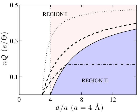
meaning that in the plot of vs (see Fig. 5) there is a separation of two regions, one with conventional electron-hole formation, the other without it. As expected, the boundary line hits the line at , the critical thickness for the appearance of electron-hole pairs in the absence of redox defects. It is important to note here that the energy will be continuous across the boundary between regions, albeit its derivative will not.
Let us now find the equilibrium concentration of surface redox defects.
4.1.1 Region I: .
Consider first the region in which there is no electronic reconstruction, . The energy becomes:
| (26) |
and is found as ever:
| (27) |
as already presented in Ref. [71]. In this case, there is a critical thickness for the onset of redox screening, i.e., when , which happens at the critical thickness
| (28) |
which is relevant only while in the regime. That means that is meaningful as such if smaller than . Using their definitions, this happens when . In practice this corresponds to cases where the redox process is energetically more favoured than the creation of electron-hole pairs in zero-field.
The parameter is expected to be small [71], therefore let us see what happens for . Then
| (29) |
which, if compared with Eq. 25, shows that the equilibrium redox defect density runs parallel to the boundary between the two regions ( and ), asymptotically as towards .
For , the onset is still the same, at , and the curve still tends asymptotically to as . However, the behaviour in between is not , and the value of pushes the curve down and makes it cross the boundary at some thickness . Such crossing can be obtained by finding the thickness for which equals the boundary density, Eq. 25,
| (30) |
which, using Eq. 27, gives
| (31) |
This last equation becomes clearer when written as follows
| (32) |
where
| (33) |
For the crossing we seek, , we then need that (which happens whenever ), and we need the denominator to be positive, i.e.,
| (34) |
This means that if the onset for redox defect stabilisation happens before the onset for electron-hole pair formation, the equilibrium line will remain in region I (no additional electron-hole formation, ) for all thicknesses, unless the surface defect mutual repulsion is strong enough. In this case of the free charge at the interface is simply and can reach rather quickly. It is interesting to briefly note here a comparison with the experimental results in ref. [70], where complete screening of the electric field was inferred through the electrostriction effect for films as thin as 6 LAO perovskite layers.
It remains to be seen what happens if the equilibrium line crosses to region II, or if the onset was already in region II, or, even if there is an equilibrium line always in region I, whether there may be another in region II. Before we get there, let us find the value of at the crossing point. For that we introduce the value of of Eq. 31 into as in Eq. 30,
| (35) |
which yields
| (36) |
which is below the asymptotic limit of if , and hence consistent with the previous discussion leading to Eq 34.
4.1.2 Region II:
In this region the equilibrium electron-hole planar density is the one given by Eq. 24 in the previous section. We now find the equilibrium density of redox defects by minimising (in Eq. 22) with respect to :
| (37) |
Introducing and solving, we obtain
| (38) |
which is thickness independent and coincides with the boundary value of coming from region I (see Eq. 36). This means that if of region I crosses the boundary, it continues horizontally into region II. If, on the other hand it does not cross, then there is no minimum for in region II (if , then gives a value beyond ), and the complete solution found in region I remains unique.
Finally, if the onset of defect formation happens for thicker samples than the onset for electron transfer, i.e. , then the equilibrium in region II becomes negative for all thicknesses, meaning that always, i.e. no redox defects appear. In this case we recover the solution of the previous section, .
4.2 Comparison with first-principles calculations
4.2.1 Formation energy of redox defects
The energy within sections 3 and 4 accounts for the formation energy of both redox defects and electron-hole pairs. Sometimes there is interest in the energies themselves (for instance, if comparing with electronic structure calculations). Depending on what is being compared, the relevant energy may be the energy of the system with redox defects referred to the energy the system would have if only allowing for electronic transfer. In that case the relevant energy is
| (39) |
It does not affect the equilibrium concentrations for , since we are just adding an -independent energy to what we had. The only difference in the analysis is that there would be a discontinuity in the derivative of the energy at because of there being a kink in . It is indicated in Fig. 5 by a vertical dotted line, effectively defining a third region. The resulting energy in the different regions is
| (40) |
4.2.2 Formation energy of one redox defect
Given the fact that is the energy for a given density of defects , the formation energy of one redox defect in an infinite system with a defect density would be
| (41) |

However, to compute the formation energy of one redox defect from first-principles one would calculate the difference in energy between a thin film with one redox defect in a given supercell, which defines the concentration , and the energy of the same supercell without the defect. That quantity we will call , and relates to the previous magnitudes in the following way:
| (42) |
which results in
| (43) |
Figure 6 shows the for various concentrations, as a function of the thickness , where it is compared with several surface vacancy formation energies obtained from first principles [98, 99]. The agreement is remarkable taking into account that the parameters could be independently computed ( is hard to pin in comparisons with experiments since it contains the chemical potential, which is hard to establish; but it is easier in comparison with calculations where the energy of the reference structures is well defined; see the Appendix in Ref. [71]). The formation of surface oxygen vacancies in LAO-STO has been further ratified within the careful calculations of ref. [104] only for the ideal concentration of oxygen vacancies, without considering oxygen vacancy concentration dependence.
4.3 Generalisation
The situation described in this section can be seen as that of competing screening mechanisms to the depolarising field, both and being positive definite, and both with their respective energy thresholds. One can think of the general screening of a thin film by different such mechanisms by rewriting Eq. 22 as
| (44) |
In the case of electronic reconstruction the quadratic term can also be included, as , the inverse density of states, accounting for the kinetic energy of the carriers, as discussed in Sections 3.1 and 3.2.
Similarly, this generalised energy could include bilinear couplings in the different variables, as . In the case of and , if the energy in Eq. 22 had an added term , the equilibrium electron density (Eqs. 24) would read
| (45) |
and the phase boundary (in Eq. 25) given by the condition would transform into
| (46) |
Such a term would describe the change in effective gap when in the presence of surface carriers due to the electronic reconstruction. It is important to state now, however, that under such interactions it is possible that the relevant defects would cluster, an effect beyond the mean-field description implied in the equations. This discussion will not be pursued any further here.
4.4 Experimental signatures and discussion
We conclude this section with a summary of experimental evidence for and against the redox screening mechanism. We concentrate on the LAO-STO system for which there are numerous studies for comparison.
The first expectation from redox screening is obviously that the surface remains insulating (except for ionic diffusion) since it is charge compensated by bound charge centres (e.g. oxygen vacancies), whilst the interface is screened by electrons (which may or may not be mobile). As already mentioned, hole conduction at the LAO surface has not been found for any thickness of LAO, whilst electronic conduction appears at the LAO-STO interface at 4 unit cells of LAO or more [7]. Ti 3 like states (Ti 3+) have been observed from spectroscopic measurements even below the 4 unit cells critical thickness, and as thin as just 1 unit cell [28, 29, 30, 32]. This suggests the possibility of the redox screening mechanism appearing almost immediately with LAO growth, since with the purely electronic reconstruction one would expect surface hole conduction and only an electronic transfer to the interface once LAO is approximately 4-6 unit cells thick (see section 3). It is indeed shown in ref. [71] following the same recipe as in section 4 that the formation of surface oxygen vacancies in LAO-STO is likely to occur for LAO films as thin as 1-3 unit cells thick.
The rapidly increasing interface electron density with film thickness predicted within the redox model (for a certain range of ) is consistent with the experimental results in ref. [70], where nearly complete screening of the electric field was inferred through the electrostriction effect for films as thin as 6 LAO perovskite layers. This is too thin to be explained by the electronic reconstruction model alone.
If redox formation is indeed responsible for the observed Ti 3 states, the next question is why for films thinner than 4 unit cells are these electrons not available for conduction. We briefly mention three possibilities that come to mind. Firstly it has been suggested that the 2DEG lies in several Ti 3 sub-bands, some of which are not mobile due to Anderson localisation [105]. The other two mechanisms are related to the experimental observation that the immobile Ti 3 levels are ‘in-gap’ states [106, 107, 108, 33] at higher binding energies. The second possibility is that acceptor defect levels are formed during the LAO growth process, such as from cation intermixing (see section 5). Cation intermixing has been readily observed in most LAO-STO samples [25, 109, 110, 111, 68, 112, 113, 114, 115].
The third possibility is that such states could be formed from the point charge of the surface redox defects which generate trapping potentials as discussed in ref. [71]. As the LAO film thickness increases the traps change from deep and few to shallow and overlapping. Hence a transition from insulating to conducting occurs at larger LAO film thickness than the redox formation itself. The character of the transition would depend on the charge of the redox defects . For even (as in the double-donor case of the oxygen vacancies), the transtion would be that of band overlap, whenever the band of filled states would touch the bottom of the conduction band. For odd (as in the case of OH- defects) the partly filled gap states would undergo an insulator to metal transition of the Mott-Anderson type [71].
Several other recent experimental findings, some of which incompatible with the electronic reconstruction, find natural explanation within the redox screening model. XPS measurements have found very little, if any, evidence for core level broadening or shift with increasing film thickness [35, 32, 36] at odds with what one might expect from a constant electric field within LAO before the electronic reconstruction critical thickness. Within the redox screening model, it can be trivially shown that the potential drop across the LAO film is essentially independent of thickness (if is small) [71]. Using the parameters for LAO-STO the potential drop for each LAO layer added was predicted to be between 0.0 and 0.2 eV [71], much smaller than within the electronic reconstruction model (approximately 0.7-0.9 eV). The predicted pinning of the potential drop (and hence reduction in electric field with thickness) is also consistent with the reduced cation-anion buckling with increasing LAO thickness as observed by SXRD [68].
Finally we note the observation that the field effect switching of the LAO-STO conductivity [7, 8] is intimately linked with surface charge writing [116, 117] and that the process is dependent on the existence of water in the surface environment [118]. These experiments are likely linked with electrochemical processes [119, 120], and are all compatible with the redox screening model. Applying a biased tip to the surface alters the field across the LAO film which either increases or decreases the stability of surface redox defects (and hence interface charge carriers and surface charge) depending on the sign of the bias. Such electrochemical processes have also been predicted during the switching of ferroelectric thin films [121, 122, 123, 124, 125].
5 Interface effects
So far we have assumed perfect interfaces and thin two-dimensional charge distributions. In this section we explore the effect on the phenomenology of deviations from such assumptions.
5.1 Interface dipole due to the electrons
The free carriers at the interface do screen (some of) the chemical charge at the interface, but their quantum spread in generates an interface dipole that has been proposed to alter the relative alignments between LAO surface and STO’s bottom of the conduction band. This effect is well described in the literature (see e.g. ref. [126] and references therein). The relevant alignment [126] is the one given by the filling of the carrier bands in the 2DEG, as illustrated in Figure 7. It depends on the zero-point energy of the band, and therefore on the perpendicular effective mass of the carriers, and on the 2DEG band filling, which depends on the carrier density and the parallel effective mass of the carriers. Discussions on the character of the 2DEG bands and corresponding effective masses are beyond the scope of this review.
5.2 Interface cation intermixing
Both during and after sample growth there is the possibility of inter-diffusion of atoms across the interface. Such processes have attracted attention lately [25, 68, 109, 110, 111, 112, 113, 114] as one of the possible explanations for the origin of 2D conduction in LAO/STO interfaces [21]. The argument used is simply that, since La is a known dopant (donor) in STO, La cations diffusing from LAO into STO could dope the interface and thus make it conducting.
Let us consider here what to expect from ions exchanging across the interface666In what follows we will make two approximations to simplify discussions, both of which can be trivially added to the models. Firstly we take the pristine interface dipole to be zero, and secondly we make the approximation that the dielectric constant is unaltered by inter-diffusion across the interface.. This discussion will focus on the effects of having a given inter-diffusion profile in a sample, rather than the energetics and kinetics that might originate it, since equilibrium is not expected to be reached in this aspect. We shall concentrate here on inter-diffusion situations starting from the pristine stoichiometric interface, and all the exchanges happening within a region around the interface whose width is smaller than other length scales in the problem. The effects on deviations from stoichiometry, and of diffusion processes from/to reservoirs extrinsic to the interface, are qualitatively different and will be treated briefly in section 5.3.
5.2.1 Interface doping generated by inter-diffusion
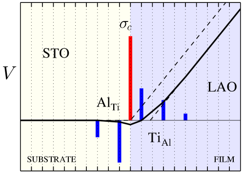
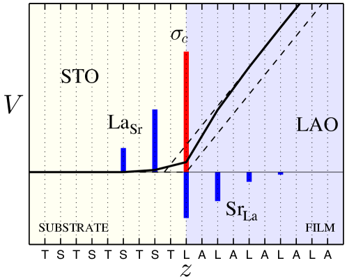
Based on chemical (steric) arguments and on quite a wealth of accumulated knowledge on perovskites, the most likely inter-diffusion processes by far are swaps of like atoms, namely, cations (Al3+ cations in LAO substituted by Ti4+, and Ti4+ in STO substituted by Al3+) and cations (La3+ to Sr2+ on one side, Sr2+ to La3+ on the other). The swap of O2- anions across the interface is also likely, but of no consequence.
Each cation substitution gives rise to a net bound charge plus a compensating carrier. La3+ replacing Sr2+ gives a centre with an associated electron, thus the donor mentioned in the previous subsection, and so do the other substitutions with obvious sign for their charges.
The first important point to make here is that such inter-diffusion should not be expected to dope the interface. Be it or cations swapping across the interface, there will be as many “wrong” cations on one side as on the other, and thus as many donors at one side as acceptors at the other. The electrons of the donors annihilate with the holes of acceptors, as long as both dopants are located in the proximity of the interface, the situation considered here. Similarly, there will be as many Ti4+ donors in LAO as Al3+ acceptors in STO. The inter-diffusion will then originate a distribution of fairly immobile charges at both sides of the interface, with zero total charge, since there are as many ’s as ’s. Indeed it is well known that the LAO-STO solid solution is insulating.
While intermixing is not expected to dope the interface, it can have implications for the transport properties and critical thickness of an interface 2DEG appearing by means of another mechanism. This is likely since the intermixing can produce the aforementioned trapping acceptor states lying below the conduction band of the pristine interface.
5.2.2 Electric field, interface dipole and interface shift
The second important point to make here is that such inter-diffusion does affect the electrostatics, but only in the interface region. It does not affect the electric field emanating from it into the film. This is a direct consequence of Gauss’s law: the net flux of the electric displacement field across surfaces parallel to the interface equals the net charge contained in the region within them. In the absence of charges diffusing in from other regions, the net charge per unit area is still , and the field emanating from the interface into the film is again , (the field in the substrate being zero).
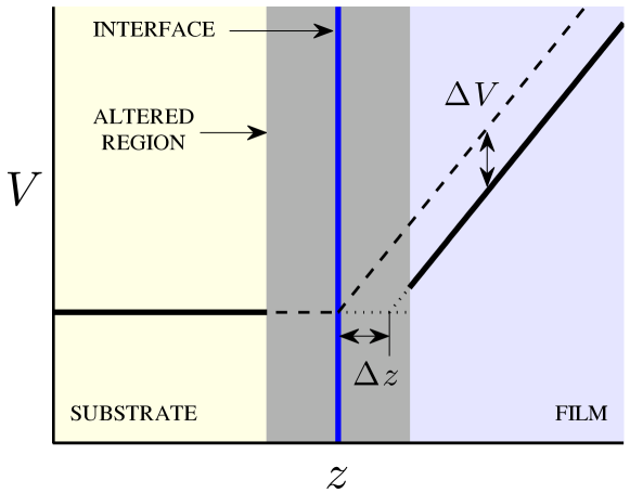
The main effect of cation inter-diffusion across the interface is illustrated in Figure 8: the electrostatic potential is shifted with respect to the one arising from a pristine interface. It is essentially the effect of the interface dipole generated by the swap of charges with its characteristic potential drop (or raise). Alternatively, this effect can be interpreted as an effective shift of the interface position, in the figure. This can be a productive way of seeing it, renormalising the film thickness in the analysis in sections 1-4.
5.2.3 Sign of the dipole and shift
The third point in this section is on the sign of such effect. Figure 9 shows quantitative examples for the behaviour of the electrostatic potential energy for electrons in two cases of inter-diffusion, one for cation exchange the other for . The former, having Al and Ti ions exchanged, produces a voltage drop, or a right shift of the effective interface position, and would thus renormalise the film thickness to a smaller value. The latter produces the opposite. From a thermodynamic point of view, cation inter-diffusion will be favoured by the electrostatics, whilst cation inter-diffusion will tend to be suppressed 777Remember these arguments are based on the original assumption of zero pristine interface dipole. A large non-zero pristine dipole of appropriate sign can reverse this trend..
5.2.4 Scale of the interface shift
The fourth point is on the scale of interface shifts. It is obvious that they will only be noticeable if on the scale of , i.e. if inter-diffusion is sizeable compared with 50% per cation layer (inter-diffusion in the ppm scale can be happily ignored). Let us obtain a quantitative estimate for .
Let us consider the -averaged charge density associated to inter-diffusion as and for the charge at the left and the right sides of the interface, respectively. The former with support for only, the latter for (we consider the pristine interface at ). The fact that there are no external charges contributing to these densities is reflected in
| (47) |
This description allows for or cation intermixing, and for both. implies more -cation exchanges, as in the upper panel of Figure 9, while -cation exchanges dominate for negative .
The electric displacement at any position can be written as
| (48) |
The zero-field substrate boundary condition gives . Assuming linear dielectric response, the electric field anywhere is given by , and thus, the field for any negative is given by
| (49) |
The electrostatic potential for anywhere in the substrate () is
| (50) |
Defining the reference potential as , and using the previous expression for the field, we get (still for )
| (51) |
which, reordering the double integral gives
| (52) | |||||
| (53) | |||||
| (54) |
where is the total charge integrated up to , and is the average charge position for the charge distribution up to . The total potential change within the substrate up to the interface is thus
| (55) |
indicating the average position of the diffusion charge in STO, and as defined in Eq. 47 (taking care of the sign).
Within the LAO side the potential has two additive components, namely, as originated by and . The first one gives the straight line starting at in Figure 9, the second one saturates to a constant once dies out (the sum of both giving the potential curves in the figure). The shift of potential due to in LAO is found analogously to STO, giving the total potential saturating at
| (56) |
The change in electrostatic potential energy for the electrons, as presented in Figure 9, , is thus
| (57) |
This expression reflects the dipole originated by the exchange, allowing a very intuitive interpretation of such effect. Following the definition of the sign of , -cation exchange gives positive , which is negative for -cation diffusion.
As illustrated in Fig. 8, this effect can be described as a shift in the apparent position of the interface, . Given the slope of the right-outgoing potential energy, , this gives
| (58) |
The thickness dependence of film properties, including film critical thickness, should then refer to the effective interface position, resulting in a net shift in the thickness axis of figures like Fig. 5.
One consequence of Eq. 58 is that in a system like LAO/STO, with , the width of the cation distribution in STO hardly affects the final shift 888Remember this prediction is under the original assumption that is unaltered by intermixing either side of the film which is likely inaccurate [27]. Deviations from such assumptions can be trivially added to the model. ,
| (59) |
Considering now a LAO film of thickness , this expression implies that the field across the film will be noticeably screened by cation inter-diffusion if () , i.e. a very substantial amount of Ti4+ going into LAO, and () , i.e. Ti cations penetrate the whole film. Indeed, perfect screening would only be possible if half a monolayer of Ti cations all traversed the whole film to sit on the surface, while their Al counterparts would go to the STO side staying close to the interface. Such cases were confirmed to screen the field within the calculations of refs. [109, 110, 104], and were obviously found to be quite stable and even exothermic. Whether these swaps across the whole film actually happens depends on the kinetics of the process.
5.3 Interfacial stoichiometry deviations
If in the growth process there is a cationic imbalance giving rise to a net deviation of the compositional charge, the effect is a trivial renormalisation of . Unlike the previous cases, where there were charge redistributions around the interface, with no change in the net charge, this section considers effects that alter the total interfacial charge.
Recently several studies have discussed the role of La:Al off-stoichiometries, which can be modulated by the laser parameters of the pulsed laser deposition, on the carrier density [92, 93, 94, 95, 96]. It was shown that when the La/Al ratio differs from unity by just a few percent, the carrier density can drop by two orders of magnitude. It is clear that cation vacancies will affect , induce acceptor states and hence reduce the interface carrier density. A concentration of just 2% -site vacancies across the whole of a LAO film of 10 unit cells would correspond to a charge close to the half a quantum 0.5 . Further discussion is beyond the scope of this paper and we refer the reader to more detailed studies [127, 128] of various types of non-stoichiometric LAO-STO systems.
These studies show that several types of defect structures are thermodynamically stable, for example the combined La vacancy at the LaO interface and O vacancy at the AlO2 surface, which screen the internal electric field and in some cases remove the interface carriers. In fact, this last kind of combined defects at surface and interface represent a similar charge screening mechanism to the ones modelled within this review: instead of the scenario of surface O vacancies and interface free electron carriers, it is surface O vacancies and interface cation vacancies. The equilibrium occurrence of such combined defects can be treated with the same model (the parameter would now include the combined formation energy of both defects), but the key difference is that this mechanism does not produce carriers for the 2DEG.
It is likely that in several systems there also exists a total deficit of oxygen, via the creation of oxygen vacancies in the substrate during the growth process or by other means, even if they are not stabilised or favoured by the electrostatics. Here each vacancy, which is likely created near the substrate surface, creates two electrons which are loosely bound near the vacancy. These processes have been suggested to play a role in LAO-STO when grown under insufficient oxygen partial pressure [6]. They may also be created at the bare STO surface when subject to ultraviolet light irradiation [129] or vacuum cleaved [130].
The unexpected conductivity observed at the non-polar interface between an amorphous LAO film and a crystalline STO substrate [54, 131, 132, 133, 134] has recently also been explained as the creation of oxygen vacancies in the STO substrate during the growth process [132, 134]. If the system is subjected to post-growth annealing in oxygen, which presumably removes these vacancies, the conductivity is no longer observed [134]. These processes are also possibly happening in other heteroepitaxial non-polar oxide systems [135].
Interestingly alterations in the net charge can also arise if there are half-unit-cell steps at the interface, with both and interface terraces. In such case there is a continuous variation of , from to , depending on the ratio of interface area covered by each kind, including a total removal of the polarisation discontinuity for the case of the interface being composed by half and half interfaces. For the cancellation to be effective, though, the width of the terraces should be smaller than the film thickness.
6 Summary
In this paper we have reviewed the present understanding on the origin of a 2DEG observed at the epitaxial interface between certain perovskite insulator thin films and certain perovskite insulator substrates, referring mostly to the paradigmatic case of an LAO film on STO. The “polar catastrophe” concept and existing evidence for and against it have been reviewed. The polarisation discontinuity of half a quantum of polarisation (for LAO on STO) is obtained from the surface theorem of Ref. [43], and the symmetry of the bulk systems. This construction is related to other symmetry-protected topological phases appearing in other contexts, namely, the topological insulators related to other symmetries as time reversal and/or particle-hole symmetry. The discussion is generalised from the conventional (001) orientation of the interface to any orientation via the lattice of meaningful polarisation vectors for these insulators, including high-index vicinal (stepped) interfaces. Alternative descriptions and formulations for the polar discontinuity found in the literature are reviewed and compared with the one based on formal polarisation.
The polar catastrophe makes the pristine film unstable towards electric-field screening mechanisms based on surface and interface charges, the latter being the electron carriers of the 2DEG. The review of such instabilities is upheld by a simple model, following on Refs. [41, 39], starting from the electronic reconstruction, followed by the redox-defect model, and their possible coexistence. The model is generalised to arbitrary homogeneous surface-interface charging mechanisms.
Finally, the effect of deviations from the ideal epitaxial growth (interface effects) are reviewed, distinguishing between deviations respecting stoichiometry (such as inter-diffusion across the interface), which do not alter the qualitative situation described by the polar catastrophe and surface-interface charge screening, and deviations that do alter stoichiometry on a substantial scale.
References
References
- [1] Ohtomo A and Hwang H Y 2004 Nature 427 423–426
- [2] Brinkman A, Huijben M, Van Zalk M, Huijben J, Zeitler U, Maan J C, Van der Wiel W G, Rijnders G, Blank D H A and Hilgenkamp H 2007 Nat. Mater. 6 493–496
- [3] Reyren N, Thiel S, Caviglia A D, Kourkoutis L F, Hammerl G, Richter C, Schneider C W, Kopp T, Ruetschi A S, Jaccard D, Gabay M, Muller D A, Triscone J M and Mannhart J 2007 Science 317 1196–1199
- [4] Bert J, Kalisky B, Bell C, Kim M, Hikita Y, Hwang H and Moler K 2011 Nature Physics 7 767–771
- [5] Li L, Richter C, Mannhart J and Ashoori R 2011 Nature Physics 7 762
- [6] Basletic M, Maurice J L, Carretero C, Herranz G, Copie O, Bibes M, Jacquet E, Bouzehouane K, Fusil S and Barthelemy A 2008 Nat. Mater. 7 621–625
- [7] Thiel S, Hammerl G, Schmehl A, Schneider C W and Mannhart J 2006 Science 313 1942–1945
- [8] Cen C, Thiel S, Hammerl G, Schneider C W, Andersen K E, Hellberg C S, Mannhart J and Levy J 2008 Nat. Mater. 7 298–302
- [9] Xie Y, Hikita Y, Bell C and Hwang H 2011 Nature Communications 2 494
- [10] Irvin P, Ma Y, Bogorin D, Cen C, Bark C, Folkman C, Eom C and Levy J 2010 Nature Photonics 4 849–852
- [11] Pallecchi I, Codda M, d’Agliano E G, Marré D, Caviglia A, Reyren N, Gariglio S and Triscone J M 2010 Phys. Rev. B 81 085414
- [12] Filippetti A, Delugas P, Verstraete M, Pallecchi I, Gadaleta A, Marré D, Li D, Gariglio S and Fiorentini V 2012 Phys. Rev. B 86 195301
- [13] Assmann E, Blaha P, Laskowski R, Held K, Okamoto S and Sangiovanni G 2013 Phys. Rev. Lett. 110 078701
- [14] Liang H, Cheng L, Zhai X, Pan N, Guo H, Zhao J, Zhang H, Li L, Zhang X, Wang X et al. 2013 Scientific reports 3
- [15] Hwang H Y 2006 Science 313 1895–1896
- [16] Pauli S A and Willmott P R 2008 J. Phys.: Condens. Matter 20 264012
- [17] Huijben M, Brinkman A, Koster G, Rijnders G, Hilgenkamp H and Blank D 2009 Adv. Mater 21 1665–1677
- [18] Mannhart J and Schlom D 2010 Science 327 1607
- [19] Pentcheva R and Pickett W 2010 J. Phys.: Condens. Matter 22 043001
- [20] Chen H, Kolpak A M and Ismail-Beigi S 2010 Advanced Materials 22 2881–2899
- [21] Schlom D and Mannhart J 2011 Nat. Mater. 10 168–169
- [22] Chambers S A 2011 Surf. Sci. 605 1133–1140
- [23] Pentcheva R, Arras R, Otte K, Ruiz V and Pickett W 2012 Phil.Trans. R. Soc. A 370 4904–4926
- [24] Gabay M, Gariglio S, Triscone J M and Santander-Syro A 2013 The European Physical Journal Special Topics 222 1177–1183
- [25] Nakagawa N, Hwang H and Muller D 2006 Nat. Mater. 5 204–209
- [26] Janotti A, Bjaalie L, Gordon L and Van de Walle C 2012 Phys. Rev. B 86 241108
- [27] Reinle-Schmitt M, Cancellieri C, Li D, Fontaine D, Medarde M, Pomjakushina E, Schneider C, Gariglio S, Ghosez P, Triscone J M et al. 2012 Nature Communications 3 932
- [28] Sing M, Berner G, Goß K, Müller A, Ruff A, Wetscherek A, Thiel S, Mannhart J, Pauli S, Schneider C, Willmott P R, Gorgoi M, Schafers F and Claessen R 2009 Phys. Rev. Lett. 102 176805
- [29] Berner G, Glawion S, Walde J, Pfaff F, Hollmark H, Duda L, Paetel S, Richter C, Mannhart J, Sing M and Claessen R 2010 Phys. Rev. B 82 241405
- [30] Takizawa M, Tsuda S, Susaki T, Hwang H Y and Fujimori A 2011 Phys. Rev. B 84(24) 245124
- [31] Rubano A, Fiebig M, Paparo D, Marino A, Maccariello D, di Uccio U S, Granozio F M, Marrucci L, Richter C, Paetel S et al. 2011 Phys. Rev. B 83 155405
- [32] Slooten E, Zhong Z, Molegraaf H, Eerkes P, de Jong S, Massee F, van Heumen E, Kruize M, Wenderich S, Kleibeuker J et al. 2013 Phys. Rev. B 87 085128
- [33] Berner G, Sing M, Fujiwara H, Yasui A, Saitoh Y, Yamasaki A, Nishitani Y, Sekiyama A, Pavlenko N, Kopp T et al. 2013 Phys. Rev. Lett. 110 247601
- [34] Plumb N, Kobayashi M, Salluzzo M, Razzoli E, Matt C, Strocov V, Zhou K J, Monney C, Schmitt T, Shi M et al. 2013 arXiv preprint arXiv:1304.5948
- [35] Segal Y, Ngai J, Reiner J, Walker F and Ahn C 2009 Phys. Rev. B 80 241107
- [36] Berner G, Müller A, Pfaff F, Walde J, Richter C, Mannhart J, Thiess S, Gloskovskii A, Drube W, Sing M et al. 2013 Phys Rev. B 88 115111
- [37] Herranz G, Basletic M, Bibes M, Carretero C, Tafra E, Jacquet E, Bouzehouane K, Deranlot C, Hamzic A, Broto J M, Barthelemy A and Fert A 2007 Phys. Rev. Lett. 98
- [38] Kalabukhov A, Boikov Y, Serenkov I, Sakharov V, Börjesson J, Ljustina N, Olsson E, Winkler D and Claeson T 2011 EPL (Europhys. Lett.) 93 37001
- [39] Bristowe N C, Littlewood P B and Artacho E 2011 J. Phys.: Condens. Matter 23 081001
- [40] Stengel M 2011 Phys. Rev. B 84(20) 205432
- [41] Bristowe N, Artacho E and Littlewood P 2009 Phys. Rev. B 80 045425
- [42] Stengel M and Vanderbilt D 2009 Phys. Rev. B 80 241103
- [43] Vanderbilt D and King-Smith R 1993 Phys. Rev. B 48 4442–4455
- [44] Murray É and Vanderbilt D 2009 Phys. Rev. B 79 100102
- [45] Goniakowski J, Finocchi F and Noguera C 2008 Rep. Prog. Phys. 71
- [46] King-Smith R D and Vanderbilt D 1993 Phys. Rev. B 47 1651–1654
- [47] Marzari N and Vanderbilt D 1997 Phys. Rev. B 56 12847–12865
- [48] Qi X L 2012 Science 338 1550–1551
- [49] Resta R 1994 Rev. Mod. Phys. 66 899
- [50] Berry M 1984 Proc. Royal Soc. London. A 392 45
- [51] Bristowe N, Stengel M, Littlewood P, Artacho E and Pruneda J 2012 arXiv preprint arXiv:1210.2278
- [52] Jadaun P, Xiao D, Niu Q and Banerjee S K 2012 arXiv.org arXiv:1208.1472
- [53] Fu L 2011 Phys. Rev. Lett. 106 106802
- [54] Herranz G, Sánchez F, Dix N, Scigaj M and Fontcuberta J 2012 Scientific reports 2
- [55] Annadi A, Zhang Q, Wang X R, Tuzla N, Gopinadhan K, Lü W, Barman A R, Liu Z, Srivastava A, Saha S et al. 2013 Nature Commun. 4 1838
- [56] Bottin F, Finocchi F and Noguera C 2005 Surf. Sci. 574 65–76
- [57] Bristowe N C, Fix T, Blamire M G, Littlewood P B and Artacho E 2012 Phys. Rev. Lett. 108(16) 166802
- [58] Cooper V R 2012 Phys. Rev. B 85 235109
- [59] Born M and Huang K 1954 Dynamical theory of crystal lattices (Oxford University Press)
- [60] Tasker P 1979 Journal of Physics C: Solid State Physics 12 4977
- [61] Harrison W A, Kraut E A, Waldrop J R and Grant R W 1978 Phys. Rev. B 18 4402–4410
- [62] Bader R F W 1990 Atoms in Molecules - A Quantum Theory (Oxford University Press)
- [63] Ghosez P, Michenaud J P and Gonze X 1998 Phys. Rev. B 58 6224
- [64] Finnis M 1998 Physica status solidi (a) 166 397–416
- [65] Ishibashi S and Terakura K 2008 J. Phys. Soc. Jpn. 77
- [66] Pentcheva R and Pickett W E 2008 Phys. Rev. B 78 205106
- [67] Pentcheva R and Pickett W 2009 Phys. Rev. Lett. 102 107602
- [68] Pauli S A, Leake S J, Delley B, Björck M, Schneider C W, Schlepütz C M, Martoccia D, Paetel S, Mannhart J and Willmott P R 2011 Phys. Rev. Lett. 106 036101
- [69] Cantoni C, Gazquez J, Miletto Granozio F, Oxley M P, Varela M, Lupini A R, Pennycook S J, Aruta C, di Uccio U S, Perna P et al. 2012 Advanced Materials 24 3952–3957
- [70] Cancellieri C, Fontaine D, Gariglio S, Reyren N, Caviglia A, Fête A, Leake S, Pauli S, Willmott P, Stengel M, Ghosez P and Triscone J 2011 Phys. Rev. Lett. 107 56102
- [71] Bristowe N C, Littlewood P B and Artacho E 2011 Phys. Rev. B 83 205405
- [72] Lee J and Demkov A A 2008 Phys. Rev. B 78 193104
- [73] Son W, Cho E, Lee B, Lee J and Han S 2009 Phys. Rev. B 79 245411
- [74] Zhu X J, Littlewood P B, Hybertsen M S and Rice T M 1995 Phys. Rev. Lett. 74 1633–1636
- [75] Zhu X J, Hybertsen M S and Littlewood P B 1996 Phys. Rev. B 54 13575–13580
- [76] Arras R, Ruiz V G, Pickett W E and Pentcheva R 2012 Phys. Rev. B 85 125404
- [77] Cazorla C and Stengel M 2012 Phys. Rev. B 85 075426
- [78] Singh-Bhalla G, Bell C, Ravichandran J, Siemons W, Hikita Y, Salahuddin S, Hebard A, Hwang H and Ramesh R 2010 Nature Physics 7 80–86
- [79] Delugas P, Filippetti A, Fiorentini V, Bilc D I, Fontaine D and Ghosez P 2011 Phys. Rev. Lett. 106 166807
- [80] Chen H, Kolpak A M and Ismail-Beigi S 2009 Phys. Rev. B 79 161402
- [81] Cancellieri C, Reyren N, Gariglio S, Caviglia A, Fête A and Triscone J 2010 EPL (Europhys. Lett.) 91 17004
- [82] Cancellieri C, Reinle-Schmitt M, Kobayashi M, Strocov V, Schmitt T, Willmott P, Gariglio S and Triscone J M 2013 Phys. Rev. Lett. 110 137601
- [83] Huang B C, Chiu Y P, Huang P C, Wang W C, Tra V T, Yang J C, He Q, Lin J Y, Chang C S and Chu Y H 2012 Phys. Rev. Lett. 109 246807
- [84] Ohtomo A, Muller D, Grazul J and Hwang H 2002 Nature 419 378–380
- [85] Perna P, Maccariello D, Radovic M, Scotti di Uccio U, Pallecchi I, Codda M, Marre D, Cantoni C, Gazquez J and Varela M 2010 Appl. Phys. Lett. 97 152111–152111
- [86] Hotta Y, Susaki T and Hwang H 2007 Phys. Rev. Lett. 99 236805
- [87] Oja R, Tyunina M, Yao L, Pinomaa T, Kocourek T, Dejneka A, Stupakov O, Jelinek M, Trepakov V, van Dijken S et al. 2012 Phys. Rev. Lett. 109 127207
- [88] Moetakef P, Cain T A, Ouellette D G, Zhang J Y, Klenov D O, Janotti A, Van de Walle C G, Rajan S, Allen S J and Stemmer S 2011 Appl. Phys. Lett. 99 232116–232116
- [89] Pentcheva R, Huijben M, Otte K, Pickett W, Kleibeuker J, Huijben J, Boschker H, Kockmann D, Siemons W, Koster G, Zandvliet H, Rijnders G, Blank D, Hilgenkamp H and Brinkman A 2010 Phys. Rev. Lett. 104 166804
- [90] Huijben M, Kockmann D, Huijben J, Kleibeuker J, van Houselt A, Koster G, Blank D, Hilgenkamp H, Rijnders G, Brinkman A et al. 2012 Phys. Rev. B 86 035140
- [91] Pentcheva R and Pickett W E 2006 Phys. Rev. B 74 035112
- [92] Schoofs F, Fix T, Kalabukhov A, Winkler D, Boikov Y, Serenkov I, Sakharov V, Claeson T, MacManus-Driscoll J and Blamire M 2011 J. Phys.: Condens. Matter 23 305002
- [93] Sato H, Bell C, Hikita Y and Hwang H 2013 arXiv preprint arXiv:1304.7830
- [94] Dildar I, Boltje D, Hesselberth M, Aarts J, Xu Q, Zandbergen H and Harkema S 2013 Appl. Phys. Lett. 102 121601–121601
- [95] Breckenfeld E, Bronn N, Karthik J, Damodaran A, Lee S, Mason N and Martin L 2013 Phys. Rev. Lett. 110 196804
- [96] Warusawithana M, Richter C, Mundy J, Roy P, Ludwig J, Paetel S, Heeg T, Pawlicki A, Kourkoutis L, Zheng M et al. 2013 Nature Commun. 4
- [97] Qiao L, Droubay T, Varga T, Bowden M E, Shutthanandan V, Zhu Z, Kaspar T C and Chambers S A 2011 Phys. Rev. B 83 085408
- [98] Li Y, Phattalung S, Limpijumnong S and Yu J 2009 Arxiv preprint arXiv:0912.4805
- [99] Li Y, Phattalung S N, Limpijumnong S, Kim J and Yu J 2011 Phys. Rev. B 84 245307
- [100] Zhong Z, Xu P and Kelly P 2010 Phys. Rev. B 82 165127
- [101] Li Y and Yu J 2013 J. Phys.: Condens. Matter 25 265004
- [102] Delugas P, Fiorentini V and Filippetti A 2005 Phys. Rev. B 71 134302
- [103] Van Benthem K, Elsasser C and French R 2001 J. Appl. Phys. 90 6156–6164
- [104] Yu L and Zunger A 2014 arXiv preprint arXiv:1402.0895
- [105] Popovic Z S, Satpathy S and Martin R M 2008 Phys. Rev. Lett. 101 256801
- [106] Drera G, Banfi F, Canova F, Borghetti P, Sangaletti L, Bondino F, Magnano E, Huijben J, Huijben M, Rijnders G, Blank D, Hilgenkamp H and Brinkman A 2011 Appl. Phys. Lett. 98 2907 ISSN 0003-6951
- [107] Ristic Z, Di Capua R, Chiarella F, De Luca G, Maggio-Aprile I, Radovic M and Salluzzo M 2012 Phys. Rev. B 86 045127
- [108] Koitzsch A, Ocker J, Knupfer M, Dekker M, Dörr K, Büchner B and Hoffmann P 2011 Phys. Rev. B 84 245121
- [109] Chambers S, Engelhard M, Shutthanandan V, Zhu Z, Droubay T, Qiao L, Sushko P, Feng T, Lee H, Gustafsson T, Garfunkel E, Shah A, Zuo J and Ramasse Q 2010 Surf. Sci. Rep. 65 317–352
- [110] Qiao L, Droubay T, Shutthanandan V, Zhu Z, Sushko P and Chambers S 2010 J. Phys.: Condens. Matter 22 312201
- [111] Qiao L, Droubay T, Kaspar T C, Sushko P and Chambers S A 2011 Surf. Sci. 605 1381–1387
- [112] Willmott P R, Pauli S A, Herger R, Schlepuetz C M, Martoccia D, Patterson B D, Delley B, Clarke R, Kumah D, Cionca C and Yacoby Y 2007 Phys. Rev. Lett. 99
- [113] Gunkel F, Hoffmann-Eifert S, Dittmann R, Mi S, Jia C, Meuffels P and Waser R 2010 Appl. Phys. Lett. 97 012103
- [114] Kalabukhov A, Boikov Y, Serenkov I, Sakharov V, Popok V, Gunnarsson R, Börjesson J, Ljustina N, Olsson E and Winkler D 2009 Phys. Rev. Lett. 103 146101
- [115] Vonk V, Huijben J, Kukuruznyak D, Stierle A, Hilgenkamp H, Brinkman A and Harkema S 2012 Phys. Rev. B 85 045401
- [116] Xie Y, Bell C, Yajima T, Hikita Y and Hwang H 2010 Nano Lett. 930–933
- [117] Xie Y, Bell C, Hikita Y and Hwang H Y 2011 Advanced Materials 23 1744–1747
- [118] Bi F, Bogorin D, Cen C, Bark C, Park J, Eom C and Levy J 2010 Appl. Phys. Lett. 97 173110
- [119] Bark C, Sharma P, Wang Y, Baek S H, Lee S, Ryu S, Folkman C, Paudel T R, Kumar A, Kalinin S V et al. 2012 Nano Lett. 12 1765–1771
- [120] Kumar A, Arruda T M, Kim Y, Ivanov I N, Jesse S, Bark C W, Bristowe N C, Artacho E, Littlewood P B, Eom C B et al. 2012 ACS nano 6 3841–3852
- [121] Wang R, Fong D, Jiang F, Highland M, Fuoss P, Thompson C, Kolpak A, Eastman J, Streiffer S and Rappe A 2009 Phys. Rev. Lett. 102 47601
- [122] Fong D, Kolpak A, Eastman J, Streiffer S, Fuoss P, Stephenson G, Thompson C, Kim D, Choi K, Eom C, Grinberg I and Rappe A 2006 Phys. Rev. Lett. 96 127601
- [123] Spanier J, Kolpak A, Urban J, Grinberg I, Ouyang L, Yun W, Rappe A and Park H 2006 Nano Lett. 6 735–739
- [124] Stephenson G B and Highland M J 2011 Phys. Rev. B 84(6) 064107
- [125] Bristowe N, Stengel M, Littlewood P, Pruneda J and Artacho E 2012 Phys. Rev. B 85 024106
- [126] Stengel M 2011 Phys. Rev. Lett. 106 136803
- [127] Seo H and Demkov A A 2011 Phys. Rev. B 84 045440
- [128] Gu M, Wang J, Wu X and Zhang G 2012 The Journal of Physical Chemistry C 116 24993–24998
- [129] Meevasana W, King P, He R, Mo S, Hashimoto M, Tamai A, Songsiriritthigul P, Baumberger F and Shen Z 2011 Nat. Mater. 10 114–118
- [130] Santander-Syro A, Copie O, Kondo T, Fortuna F, Pailhes S, Weht R, Qiu X, Bertran F, Nicolaou A, Taleb-Ibrahimi A et al. 2011 Nature 469 189–193
- [131] Chen Y, Pryds N, Kleibeuker J E, Koster G, Sun J, Stamate E, Shen B, Rijnders G and Linderoth S 2011 Nano Lett. 11 3774–3778
- [132] Lee S W, Liu Y, Heo J and Gordon R G 2012 Nano Lett. 12 4775–4783
- [133] Christensen D, Trier F, Chen Y, Smith A, Nygard J and Pryds N 2013 Appl. Phys. Lett. 102 021602–021602
- [134] Liu Z, Li C, Lü W, Huang X, Huang Z, Zeng S, Qiu X, Huang L, Annadi A, Chen J et al. 2013 Phys. Rev. X 3 021010
- [135] Chen Y, Bovet N, Trier F, Christensen D, Qu F, Andersen N H, Kasama T, Zhang W, Giraud R, Dufouleur J et al. 2013 Nature Commun. 4 1371