Robust design by anti-optimization for parameter tolerant GaAs/AlOx High Contrast Grating mirror for VCSEL application
Abstract
A GaAs/AlOx high contrast grating structure design which exhibits a 99.5 % high reflectivity for a 425 nm large bandwidth is reported. The HCG structure has been designed in order to enhance the properties of mid-infrared VCSEL devices by replacing the top Bragg mirror of the cavity. A robust optimization algorithm has been implemented to design the high contrast grating structure not only as an efficient mirror but also as a robust structure against the imperfections of fabrication. The design method presented here can be easily adapted for other high contrast grating applications at different wavelengths.
Index Terms:
High contrast grating mirror, mid-infrared VCSEL, robust design, parameter tolerantI Introduction
High contrast gratings (HCG) are diffractive structures made of a material with a high optical index for the grating slabs surrounded by a low index material. With a high optical index contrast () and a near-wavelength grating period, the structure diffracts only into the 0 order of diffraction and can be seen as a 1D photonic crystal supporting only a few propagative Bloch modes. However, contrary to photonic crystal slabs, the modes propagate perpendicularly to the slab plane[1, 2]. The resonance of these modes between the two grating interfaces and their coupling at the interfaces can be adjusted to obtain different and very promising properties in a large range of applications[2] such as broadband mirrors[3, 4, 5, 6], high-Q resonators[7], planar lenses[8], wavefront control [9], optical isolators[10], waveplates[11], circular polarizers[12] or electromechanical mirrors[13, 14]. The mirror effect is particularly interesting since it can exhibit not only a polarization independence[15] with good angular insensitivity[16] but also a good reflectivity selectivity between TE and TM modes[3, 17]. With only one high contrast grating layer, it is thus possible to obtain a very large bandwidth of 30% for more than 99% reflectivity and even 17% for 99.9%[18].
The development of VCSEL devices emitting in the 2–3 µm wavelength range remains a challenging task today. The realization of VCSEL devices which are single-mode, low cost and tunable light sources [19] is of great interest for gas detection in the mid-infrared wavelength range where gas species such as carbon monoxide exhibit strong absorption lines[20, 21]. VCSEL structures based on InP system have demonstrated mid infrared laser emission in continuous wave (CW) at room temperature for 2.3 µm [22]. However this wavelength seems to be the maximum limit for this material system [19]. Thus several VCSEL structures based on AlGaInAsSb material system have been developed. A VCSEL structure using a buried tunnel junction for current confinement have shown CW emission at 2.36 µm up to 363 K[23] while another structure based on selective lateral etching of the tunnel junction in order to realize a current aperture have shown CW emission at 2.31 µm up to 343 K[24]. More recently, a GaSb-based VCSEL using a lateral wet oxidation of AlAs for current confinement has been demonstrated and exhibits CW laser emission at 2.38 µm for a temperature of 253 K[25]. The development of VCSEL based on AlGaInAsSb is thus a very promising solution for the mid infrared wavelength range. However, laser emission is still limited today at 2.6 µm at room temperature [26, 27]. One of the main problem at such large wavelengths is the increase of the device thickness which reaches about 12 µm since more than 20 pairs of quarter-wavelength AlSb/GaSb layers are required for the VCSEL Bragg mirrors[28].
The large and high reflectivity bandwidth, low mirror thickness and high polarization selectivity of HCG structures make them good candidates for replacement of Bragg mirrors in VCSEL diodes. VCSEL designs which use a grating as a polarizing mirror in order to enhance the laser properties have thus been proposed [29, 30]. Several VCSEL structures based on HCG have then been developed and have demonstrated laser emission with GaAs-based material around 850 nm[31] and 980 nm[32] or with InP-based material at 1320 nm[33] and 1550 nm [34, 35, 36].
The short amplification length of VCSEL structures imposes the use of a high quality mirror with reflectivity larger than 99.5 % for large bandwidths which are typically about 150 nm in mid-infrared[28]. The mirror efficiency required for VCSEL application is thus demanding and imposes a precise adjustment of HCG geometrical parameters during the design process. Even if the physic of HCG is well understood [1, 37], numerical simulations by RCWA [38] of the reflectivity of HCG structures allow the use of an optimization algorithm [39, 40, 41, 42] to design the mirror properties for a specific application.
Since VCSEL devices require high quality mirrors and HCG have sub-micrometric square-shaped patterns, the fabrication of HCG structures needs to control masking and etching process with a high accuracy in the nanometric range[42]. On the other hand, HCG mirrors can be designed to have a good robustness of several percent on the geometrical dimensions. So, to achieve a robust and efficient mirror, the tolerance with respect to the errors of fabrication has to be taken into account during the design of the structure[43, 44, 41].
In this paper, we present the design of a GaAs HCG combined with an AlOx sublayer as low index material to replace the top DBR of mid infrared GaSb-based VCSEL. In a first part, an optimization algorithm is used to find the best dimensions of the HCG structure. Then, the tolerance of the geometrical parameters of the optimum design with respect to the errors of fabrication are numerically investigated. In a second part, an anti-optimization algorithm is combined to the optimization process to develop a robust optimization algorithm. This original design approach of high contrast gratings takes into account the tolerances required by the manufacturers on the different parameters directly during the design process. The gratings mirrors are thus optimized to exhibit not only high efficiency but also large tolerance values.
II Optimization method
II-A Structure of the mirror
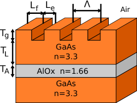
The mirror structure presented in Figure 1 is made of a GaAs grating () with a period , a thickness and a Fill Factor . The high contrast of optical index required for large bandwidth mirror is obtained thanks to the use of a low index AlOx sublayer () with a thickness . The choice of the GaAs/AlOx material system has been made in order to allow a monolithic epitaxial process during the integration of the HCG mirror in a VCSEL structure[45, 32]. The AlOx layer can be obtained from a wet oxidation process of AlAs similar to the one used for current confinement by oxide aperture in VCSEL structures[46, 47, 48]. The GaAs top layer is not completely etched during the grating fabrication resulting in a GaAs intermediate layer of thickness . The presence of an intermediate GaAs layer should enhance the mechanical stability of the grating above the AlOx layer since the oxidation process decreases the AlAs layer thickness of about 10 %[45].
HCG mirrors presented in this work are designed to be used as VCSEL top mirrors, thus in the HCG structure presented in Figure 1, the GaAs substrate corresponds to the VCSEL cavity with light propagating from substrate to the air. In order to obtain a laser cavity, a minimum reflectivity value of 99.5 % is required for VCSEL mirrors for the largest possible bandwidth. To solve the problem of polarization instability and mode hoping of VCSEL devices, the mirror is chosen to be polarization dependent by reflecting light only for the transverse magnetic mode (TM) while keeping the transverse electric (TE) reflection coefficient below a 90 % threshold.
II-B Optimization of the mirror parameters
In order to satisfy all the previously defined VCSEL requirements, the structure dimensions , , , and have to be carefully designed. An optimization algorithm has been used to automate the search of the most efficient mirror design. The efficiency of the HCG structure has been defined through the use of a figure of merit [42] which represents quantitatively the mirror quality from a VCSEL application point of view :
| (1) |
The figure of merit mainly represents the normalized bandwidth of the mirror, defined as the wavelength range around where the reflectivity is larger than 99.5 % for TM mode and below 90 % for the TE mode. The normalized bandwidth is also multiplied by a Gaussian weighted average of the transverse magnetic reflection coefficients of the bandwidth to ensure a centering around . Reflection spectra of the mirror are computed by rigorous coupled wave analysis (RCWA)[49] for transverse magnetic and transverse electric polarizations.
Several optimization algorithms can be used to design HCG structures such as simulated annealing[39], genetic algorithm[40] or particle swarm[15, 41]. Due to the presence of many local maxima, a global optimization approach is required. In this work, we have implemented a particle swarm optimization (PSO) algorithm[50] to maximize the figure of merit . The particle swarm algorithm is based on a population of particles which are candidate solutions sharing their knowledge of optimum positions when exploring the search space. The particles of the swarm, of which positions correspond to a set of the design parameters , , , , , are moved at each algorithm iteration with a velocity :
| (2) |
The velocity at the iteration of the particle of the swarm is composed of 3 terms. Firstly, the inertia of the particle is taken into account by keeping the velocity of the previous iteration . Secondly, a local velocity term moves the particle toward the local best position known by the particle . Finally, the swarm concept is created by sharing the best position of all particles thanks to the global best position which creates a global velocity term. The parameters and are two weights for the local and global velocities which are randomly chosen from a uniform law in the range at each particle move[50].
The dimensions of the mirror structure have been optimized within bounds that take technological constraints into account. The AlOx layer thickness has been shown to maximize the reflectivity for values of [45], but has been bounded between 300 nm and 400 nm to limit the optical losses within the oxide. The Fill Factor limitations are chosen with respect to the e-beam lithography and etching process and have been bounded between 35 % and 55 %. The other parameter constraints are only given to define a search space for the optimization algorithm but can also be chosen with respect to other technological limitations : 500 nm 1100 nm, 900 nm 1300 nm and 50 nm 1000 nm.
II-C Optimization results
| Differential | Particle | |
| Evolution | Swarm | |
| 685 nm | 657 nm | |
| 0.513 | 0.538 | |
| 390 nm | 352 nm | |
| 1158 nm | 1117 nm | |
| 268 nm | 283 nm | |
| 2340 nm | 2298 nm | |
| 481 nm | 493 nm | |
| 20.6 % | 21.5 % |
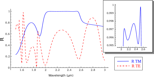
The particle swarm optimization algorithm has been executed with the previously defined parameters to design the GaAs/AlOx HCG mirror presented in Figure 1. The optimum mirror found by the algorithm exhibits a 493 nm large bandwidth with structure dimensions of 657 nm, 0.5380, 352 nm, 1117 nm and 283 nm (Table I). In order to validate the result obtained by our implementation of the particle swarm optimization, a comparison has been made with a differential evolution[51] optimization algorithm[52] under the same technological constraints for the mirror structure. The execution of the latter algorithm results in a 481 nm large bandwidth (Table I) which is equivalent to the PSO algorithm. Both points are very close and satisfy all VCSEL requirements and technological constraints. The 99.5 % high TM reflectivity and large bandwidth ( 21.5 %) of the mirror optimized by PSO exhibits a good polarization selectivity by keeping below 70 % (Figure 2). The high reflectivity performances of the GaAs/AlOx HCG structure makes it a very promising mirror for VCSEL application at 2300 nm.
II-D Tolerance of the optimum design
| Optimum | Min | Max | Tolerance | |
| 685 nm | 682 nm | 756 nm | 3 nm | |
| 0.513 | 0.507 | 0.590 | 0.006 | |
| 390 nm | 364 nm | 499 nm | 26 nm | |
| 1158 nm | 1014 nm | 1163 nm | 5 nm | |
| 268 nm | 221 nm | 272 nm | 4 nm | |
| 2340 nm | ||||
| 481nm | ||||
| 20.6 % | ||||
| Optimum | Min | Max | Tolerance | |
| 657 nm | 609 nm | 737 nm | 48 nm | |
| 0.538 | 0.418 | 0.607 | 0.069 | |
| 352 nm | 282 nm | 447 nm | 70 nm | |
| 1117 nm | 993 nm | 1148 nm | 31 nm | |
| 283 nm | 248 nm | 308 nm | 25 nm | |
| 2298 nm | ||||
| 493 nm | ||||
| 21.5 % | ||||
From a fabrication point of view, it is important to know how tolerant the structure is with respect to the error of fabrication on the different dimensions. The tolerance of one parameter is defined as the variation range for which the mirror keeps a TM reflectivity larger than 99.5 % together with a TE reflectivity smaller than 90 % at 2300 nm. The evaluation of the tolerance of one dimension of the structure is done by increasing and decreasing its optimum value while keeping all the other ones at their optimum values. It is important to note that the way the evaluation of tolerance is performed does not give any information on an error of fabrication made simultaneously on different dimensions[43].
As it has already been reported in the literature, HCG can exhibit large tolerances on the design parameters[43, 44, 41]. For instance, minimum and maximum values of the parameters of the optimum designs found by the algorithms result in variation range of more than 10 % as it can be seen in Table II and Table III. Despite large variation ranges, the tolerance value of the dimension can be as small as 3 nm for instance on the grating thickness (Table II). Such a critical tolerance value would make the etching control difficult and decrease drastically the probability of successfully etching the grating. Since the optimization algorithm will search for the most efficient design regardless of its tolerance, if an optimum is localized at the edge of the variation range, the optimization can result in a non tolerant design[43, 53].
The design of GaAs/AlOx HCG by an optimization algorithm provides very efficient mirrors with large bandwidth well adapted for VCSEL integration. However the optimization process can randomly result in a point very sensitive to the error of fabrication and can be difficult to fabricate.
III Robust optimization
III-A Anti-optimization method
In order to make the fabrication of HCG possible for a VCSEL integration, mirror structures have to be not only efficient but also robust with respect to the fabrication errors. A simple way to improve the mirror tolerance is to manually center the structure dimensions within their variation ranges[43]. However, since the tolerance is evaluated for each parameter independently, the centering within the variation range does not take into account the error made on several parameters simultaneously. The tolerance computation of combination of parameters such as , can increase the knowledge of the robustness, but the adjustment of the grating dimensions becomes complex when the number of parameters increases. Moreover, since the manual robustness enhancement can only be performed once the dimensions are optimized, the use of an optimization algorithm to make the design process easy and automated is lost.
The maximization of the figure of merit in order to find the most efficient mirror structure by an optimization algorithm can be coupled to an anti-optimization process to form a robust optimization algorithm. The purpose of anti-optimization[54] is to search for the worst scenario of fabrication of the optimum found which would result in the least efficient mirror. For that purpose, a new figure of merit has been introduced :
| (3) |
The robustness of the design is taken into account in the figure of merit for a design defined by by computing the average value of the figure of merit with the minimum of figure of merit associated to the worst scenario of fabrication. The search of the minimum is done in the hyper-space around delimited by user-defined tolerance specifications with . The last parameter of the figure of merit corresponds to a percentage of the process of tolerance evaluation. Thus, efficient mirrors which keep good performances within user-defined variation ranges will have a larger figure of merit than non tolerant structures.
The evaluation of requires to know the minimum value of within the whole tolerance area defined by . The search for this minimum could be done by an optimization algorithm but would be time consuming. Moreover, if the current point has a low value, the evaluation of its robustness would be useless since a weak solution will not be kept during the optimization. Since the particle swarm algorithm moves the particles by directing them to local and global optimum values ( and ) stored in memory, the tolerance evaluation can be done only on the best positions known by the swarm. In order to make a fast evaluation of the tolerance which does not rely on an optimization algorithm to find the worst design within the tolerance area, only the extremum values of each parameter and are computed. The estimation of the minimum used for the averaging of the in Eq. 3 is thus evaluated with only 10 points in the case of the GaAs/AlOx HCG structure and does not take into account errors made simultaneously on several parameters or a local minimum located between and for instance. In a dimension problem, with parameters to optimize, the tolerance evaluation process is done in steps for the positive and negative tolerance estimation of each parameter. The parameter in Eq. 3 represents thus the percentage of achievement of the tolerance evaluation process. At each step, the figure of merit is updated and if its value becomes lower than another point stored in memory, the anti-optimization process stops and the optimization continues to find a new optimum. A competition between optimization and anti-optimization is thus used to enhance the efficiency of the robust algorithm by decreasing the number of points evaluated and the computational cost.
To increase the reliability of the tolerance evaluation, the errors made simultaneously on several structure parameters have been taken into account by comparing the new computed design to the optimum known by the swarm. Since the particles move towards their local and global optimum, if a new minimum is computed around the optimum within the tolerance area or during the optimization process, its figure of merit will be used to adjust the figure of merit associated to or . The PSO exploration of the search space is thus used advantageously to increase the robustness by taking into account errors made simultaneously on several design parameters.
III-B Tolerance requirements and first result
The execution of the robust optimization algorithm imposes to define tolerance requirements for the mirror parameters. One of the most critical parameter to control is the oxide layer thickness since a 8–13 % decrease of the layer arises from the oxidation process of AlAs[45]. The tolerance of the AlOx layer thickness has been set to be of 50 nm during the optimization. Nevertheless, simulations have already shown that the low index sublayer thickness is not a critical parameter[45] of the HCG mirror and a 50 nm tolerance should not be a severe design constraint[42, 55]. The grating parameters and linked to the etching process are more critical and require large tolerance values of 20 nm and 0.02. The other parameters are either defined by the epitaxial growth of the structure () or by e-beam lithography () and are better controlled. Tolerance requirements for these parameters have been set to lower values with 1 nm and 3 nm.
The optimization of the GaAs/AlOx mirror with the robust optimization algorithm performed in the same conditions as described in Section II results in a structure which dimensions are given in Table IV and exhibits a 369 nm large bandwidth. A tolerance study of the mirror parameters shows that all dimensions meet the tolerance requirements and that the optimum is correctly centered within the variation ranges (Table IV). A comparison with the design optimized with the particle swarm algorithm without anti-optimization (Table III) shows that the bandwidth is 124 nm smaller for the mirror obtained by robust optimization. A decrease of tolerance values is also exhibited for and but are still larger than the requirements. However, when performing a statistical test by varying simultaneously and randomly the structure dimensions with a uniform law for the previously defined tolerance values, the failure rate ( % at ) decreases from 1.9 % from the design without robust optimization to less than 0.01 % for the robust design. Despite a decrease of bandwidth and tolerances, the robustness of the grating is still enhanced by the use of the robust optimization algorithm which improves tolerance with respect to errors made on several parameters and guarantees the resulting optimized design to meet user-defined tolerance requirements.
| Optimum | Tolerances for at | ||
| 713 nm | 682 nm 773 nm | 31 nm | |
| 0.484 | 0.403 0.548 | 0.064 | |
| 355 nm | 255 nm | 100 nm | |
| 1145 nm | 1038 nm 1206 nm | 61 nm | |
| 249 nm | 215 nm 301 nm | 34 nm | |
| 2309 nm | |||
| 369 nm | |||
| 16.0 % | |||
III-C Final robust design
The use of a robust optimization algorithm allows the search of not only the most efficient but also robust solution. However, with a 25 % decrease of the bandwidth and smaller tolerances for the critical parameters and , the optimum found by the robust optimization algorithm described in section III-A seems to be a poor result compared to the non robust optimization. The combination of the anti-optimization and the particle swarm algorithm has introduced a perturbation of the convergence of the optimization algorithm. When a new robust optimum is discovered, it could take several iterations of the algorithm to perform a good enough exploration of its neighborhood and decrease the robustness if a new minimum is found in the user defined tolerance ranges. A new optimum is then chosen by the swarm to be the best one, but its robustness has to be evaluated from scratch by the anti-optimization process and will not take into account the previously computed points.
To enhance the speed of the tolerance evaluation process of the anti-optimization, the robust optimization algorithm has been improved. Instead of using only the new points computed during the optimization to adjust the tolerance of the best known design, the minimum used in the figure of merit is made on every points computed since the start of the optimization algorithm. This requires to store in memory all the tested designs and their associated figure of merit . The process of adding a memory in the swarm allows it to remember where the designs which are sensitive to error of fabrication are located and avoid them more easily.
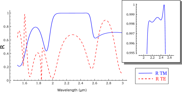
The execution of the modified robust optimization with the same technological and tolerance requirements as before returns a HCG mirror with a 425 nm large bandwidth which dimensions are given in Table V. The tolerance evaluation of the parameters shows a good robustness with an optimum value well centered within large variation range. The grating thickness and Fill Factor tolerances are very large with nm and . A statistic study with 30 000 tests of the tolerance of the optimum by varying simultaneously all the design parameters with 20 nm, 0.02, 50 nm, 3 nm and 1 nm have returned 0 mirror with less than 99.5 % of TM reflectivity at 2300 nm.
Finally, the tolerance of the optical index values of the materials have been explored. Indeed, the refractive index of the GaAs, and the AlOx especially, can vary with respect to the conditions of fabrication. Computations have shown that the high contrast grating presented in Table V exhibits a reflictivity of more than 99.5 % at for GaAs index values between 3.22 and 3.6 and AlOx index values between 1 and 1.78. Besides the variation of the refractive index, AlOx can present absorption in the mid infrared wavelength range [56]. Even though the absorption is negligible below 2.5 µm [56], the maximum absorption allowed to keep a 99.5 % reflectivity has been computed and is 110 cm-1 ().
| Optimum | Tolerances for at | ||
| 668 nm | 598 nm 738 nm | 70 nm | |
| 0.5351 | 0.4361 0.5981 | 0.063 | |
| 360 nm | 228 nm | 132 nm | |
| 1098 nm | 993 nm 1162 nm | 64 nm | |
| 282 nm | 240 nm 331 nm | 42 nm | |
| 2290 nm | |||
| 425 nm | |||
| 18.6 % | |||
IV Conclusion
A robust optimization algorithm has been developed to design high contrast grating mirrors for a VCSEL application at 2.3 µm. An anti-optimization process based on particle swarm optimization is used to adjust the geometrical parameters of the HCG structure by taking into account technological constraints. The fabrication accuracy of our equipments is also taken into account within the optimization process by defining tolerance requirements that the HCG parameters have to meet. The execution of the robust optimization algorithm thus results not only in an efficient mirror with a 99.5 % high reflectivity for a 425 nm large bandwidth but also in a robust design with more than 10 % of tolerance on the grating thickness, which is one of the most critical parameter of the grating fabrication process. The mirror also exhibits a strong polarization selectivity by keeping the reflection coefficient of the TE mode lower than 70 %. This polarization selectivity combined with high mirror efficiency and large fabrication tolerance should make the GaAs/AlOx HCG design presented in this work a very good VCSEL mirror to allow emission above 2.3 µm.
Acknowledgments
The authors thank the French ANR for financial support in the framework of Marsupilami project (ANR-09-BLAN-0166-03) and IES and LAAS (France), partners of LMOPS/Supélec in this project. This work was also partly funded by the InterCell grant (http://intercell.metz.supelec.fr) by INRIA and Région Lorraine (CPER2007).
References
- [1] P. Lalanne, J. P. Hugonin, and P. Chavel, “Optical properties of deep lamellar gratings: A coupled bloch-mode insight,” J. Lightwave Technol. 24, 2442 (2006).
- [2] C. J. Chang-Hasnain and W. Yang, “High-contrast gratings for integrated optoelectronics,” Adv. Opt. Photon. 4, 379–440 (2012).
- [3] S. Goeman, S. Boons, B. Dhoedt, K. Vandeputte, K. Caekebeke, P. Van Daele, and R. Baets, “First demonstration of highly reflective and highly polarization selective diffraction gratings (GIRO-gratings) for long-wavelength VCSELs,” Photonics Technology Letters, IEEE 10, 1205 –1207 (1998).
- [4] C. Mateus, M. Huang, L. Chen, C. Chang-Hasnain, and Y. Suzuki, “Broad-band mirror (1.12-1.62 µm) using a subwavelength grating,” Photonics Technology Letters, IEEE 16, 1676 –1678 (2004).
- [5] T. T. Wu, Y. C. Syu, S. H. Wu, W. T. Chen, T. C. Lu, S. C. Wang, H. P. Chiang, and D. P. Tsai, “Sub-wavelength GaN-based membrane high contrast grating reflectors,” Opt. Express 20, 20551–20557 (2012).
- [6] J. M. Foley, A. M. Itsuno, T. Das, S. Velicu, and J. D. Phillips, “Broadband long-wavelength infrared Si/SiO2 subwavelength grating reflector,” Opt. Lett. 37, 1523–1525 (2012).
- [7] Y. Zhou, M. Moewe, J. Kern, M. C. Huang, and C. J. Chang-Hasnain, “Surface-normal emission of a high-Q resonator using a subwavelength high-contrast grating,” Opt. Express 16, 17282–17287 (2008).
- [8] D. Fattal, J. Li, Z. Peng, M. Fiorentino, and R. G. Beausoleil, “Flat dielectric grating reflectors with focusing abilities,” Nat Photon 4, 466–470 (2010).
- [9] L. Carletti, R. Malureanu, J. Mørk, and I.-S. Chung, “High-index-contrast grating reflector with beam steering ability for the transmitted beam,” Opt. Express 19, 23567–23572 (2011).
- [10] W.-M. Ye, X.-D. Yuan, C.-C. Guo, and C. Zen, “Unidirectional transmission in non-symmetric gratings made of isotropic material,” Opt. Express 18, 7590–7595 (2010).
- [11] R. Magnusson, M. Shokooh-Saremi, and E. G. Johnson, “Guided-mode resonant wave plates,” Opt. Lett. 35, 2472–2474 (2010).
- [12] M. Mutlu, A. E. Akosman, and E. Ozbay, “Broadband circular polarizer based on high-contrast gratings,” Opt. Lett. 37, 2094–2096 (2012).
- [13] K. Hane, T. Kobayashi, F.-R. Hu, and Y. Kanamori, “Variable optical reflectance of a self-supported Si grating,” Applied Physics Letters 88, 141109 (2006).
- [14] M. C. Y. Huang, Y. Zhou, and C. J. Chang-Hasnain, “A nanoelectromechanical tunable laser,” Nat. Photon. 2, 180–184 (2008).
- [15] M. Shokooh-Saremi and R. Magnusson, “Leaky-mode resonant reflectors with extreme bandwidths,” Opt. Lett. 35, 1121–1123 (2010).
- [16] H. Wu, J. Hou, W. Mo, D. Gao, and Z. Zhou, “A multilayer-based wideband reflector utilizing a multi-subpart profile grating structure,” Journal of Optics 12, 065704 (2010).
- [17] M. Shokooh-Saremi and R. Magnusson, “Multi-level periodic leaky-mode resonance elements: Design and applications,” Optical Interference Coatings p. WB2 (2010).
- [18] C. Mateus, M. Huang, Y. Deng, A. Neureuther, and C. Chang-Hasnain, “Ultrabroadband mirror using low-index cladded subwavelength grating,” IEEE Photon. Technol. Lett. 16, 518–520 (2004).
- [19] M. Ortsiefer, W. Hofmann, J. Rosskopf, and M.-C. Amann, Long-Wavelength VCSELs with Buried Tunnel Junction, vol. 166 of Springer Series in Optical Sciences (Springer Berlin Heidelberg, 2013).
- [20] A. Ouvrard, A. Garnache, L. Cerutti, F. Genty, and D. Romanini, “Single-frequency tunable Sb-based VCSELs emitting at 2.3 µm,” IEEE Photonics Technology Letters 17, 2020–2022 (2005).
- [21] J. Chen, A. Hangauer, R. Strzoda, and M.-C. Amann, “VCSEL-based calibration-free carbon monoxide sensor at 2.3 µm with in-line reference cell,” Appl. Phys. B (2010). 10.1007/s00340-010-4011-0.
- [22] M. Ortsiefer, G. Böhm, M. Grau, K. Windhorn, E. Rönneberg, J. Rosskopf, R. Shau, O. Dier, and M. C. Amann, “Electrically pumped room temperature CW VCSELs with 2.3 m emission wavelength.” Electron. Lett. 42 (2006).
- [23] A. Bachmann, S. Arafin, K. Kashani-Shirazi, and M.-C. Amann, “Long wavelength electrically pumped GaSb-based buried tunnel junction VCSELs,” Physics Procedia 3, 1155 – 1159 (2010).
- [24] D. Sanchez, L. Cerutti, and E. Tournié, “Single-mode monolithic GaSb vertical-cavity surface-emitting laser,” Opt. Express 20, 15540–15546 (2012).
- [25] Y. Laaroussi, D. Sanchez, L. Cerutti, C. Levallois, C. Paranthoen, A. Rumeau, C. Tourte, and G. Almuneau, “Oxide-confined mid-infrared VCSELs,” Electronics Letters 48, 1616 –1618 (2012).
- [26] S. Arafin, A. Bachmann, K. Kashani-Shirazi, and M.-C. Amann, “Electrically pumped continuous-wave vertical-cavity surface-emitting lasers at 2.6 µm,” Applied Physics Letters 95, 131120 (2009).
- [27] A. Ducanchez, L. Cerutti, P. Grech, F. Genty, and E. Tournié, “Mid-infrared GaSb-based EP-VCSEL emitting at 2.63 µm.” Electron. Lett. 45, 265–267 (2009).
- [28] L. Cerutti, A. Ducanchez, G. Narcy, P. Grech, G. Boissier, A. Garnache, E. Tournié, and F. Genty, “GaSb-based VCSELs emitting in the mid-infrared wavelength range (2-3 µm) grown by MBE,” J. Cryst. Growth 311, 1912–1916 (2009).
- [29] R. Magnusson, D. Shin, and P. P. Young, “Vertical-cavity laser and laser array incorporating guided-mode resonance effects and method for making the same,” US Patent 6 154 480 A, 2000.
- [30] R. Magnusson, Y. Ding, K. J. Lee, D. Shin, P. S. Priambodo, P. P. Young, and T. A. Maldonado, “Photonic devices enabled by waveguide-mode resonance effects in periodically modulated films,” Proc. SPIE, 5225, 20–34 (2003).
- [31] M. Huang, Y. Zhou, and C. Chang-Hasnain, “A surface-emitting laser incorporating a high-index-contrast subwavelength grating,” Nat. Photon. 1, 119–122 (2007).
- [32] P. Gilet, N. Olivier, P. Grosse, K. Gilbert, A. Chelnokov, I.-S. Chung, and J. Mørk, “High-index-contrast subwavelength grating VCSEL,” pp. 76150J–76150J–8 (2010).
- [33] W. Hofmann, C. Chase, M. Müller, Y. Rao, C. Grasse, G. Böhm, M.-C. Amann, and C. Chang-Hasnain, “Long-wavelength high-contrast grating vertical-cavity surface-emitting laser,” Photonics Journal, IEEE 2, 415–422 (2010).
- [34] S. Boutami, B. Benbakir, J.-L. Leclercq, and P. Viktorovitch, “Compact and polarization controlled 1.55 µm vertical-cavity surface-emitting laser using single-layer photonic crystal mirror,” Applied Physics Letters 91, 071105 (2007).
- [35] C. Chase, Y. Rao, W. Hofmann, and C. J. Chang-Hasnain, “1550 nm high contrast grating VCSEL,” Opt. Express 18, 15461–15466 (2010).
- [36] C. Sciancalepore, B. Bakir, X. Letartre, J. Harduin, N. Olivier, C. Seassal, J. Fedeli, and P. Viktorovitch, “CMOS-compatible ultra-compact 1.55-µm emitting VCSELs using double photonic crystal mirrors,” IEEE Photon. Technol. Lett. 24, 455–457 (2012).
- [37] V. Karagodsky, F. G. Sedgwick, and C. J. Chang-Hasnain, “Theoretical analysis of subwavelength high contrast grating reflectors,” Opt. Express 18, 16973–16988 (2010).
- [38] M. G. Moharam, D. A. Pommet, E. B. Grann, and T. K. Gaylord, “Stable implementation of the rigorous coupled-wave analysis for surface-relief gratings: enhanced transmittance matrix approach,” J. Opt. Soc. Am. A 12, 1077–1086 (1995).
- [39] E. Bisaillon, D. Tan, B. Faraji, A. Kirk, L. Chrowstowski, and D. V. Plant, “High reflectivity air-bridge subwavelength grating reflector and fabry-perot cavity in AlGaAs/GaAs,” Opt. Express 14, 2573–2582 (2006).
- [40] M. Shokooh-Saremi and R. Magnusson, “Particle swarm optimization and its application to the design of diffraction grating filters,” Opt. Lett. 32, 894–896 (2007).
- [41] H. Wu, W. Mo, J. Hou, D. Gao, R. Hao, H. Jiang, R. Guo, W. Wu, and Z. Zhou, “A high performance polarization independent reflector based on a multilayered configuration grating structure,” Journal of Optics 12, 045703 (2010).
- [42] C. Chevallier, N. Fressengeas, F. Genty, and J. Jacquet, “Optimized sub-wavelength grating mirror design for mid-infrared wavelength range,” Appl. Phys. A- Mater. 103, 1139–1144 (2011).
- [43] C. Chevallier, N. Fressengeas, F. Genty, and J. Jacquet, “Optimized Si/SiO2 high contrast grating mirror design for mid-infrared wavelength range: Robustness enhancement,” Optics & Laser Technology 44, 626–630 (2012).
- [44] Y. Zhou, M. Huang, and C. Chang-Hasnain, “Large fabrication tolerance for VCSELs using high-contrast grating,” IEEE Photon. Technol. Lett. 20, 434–436 (2008).
- [45] G. Almuneau, M. Condé, O. Gauthier-Lafaye, V. Bardinal, and C. Fontaine, “High reflectivity monolithic sub-wavelength diffraction grating with GaAs/AlOx stack,” Journal of Optics 13, 015505 (2011).
- [46] D. Huffaker, D. Deppe, K. Kumar, and T. Rogers, “Native oxide defined ring contact for low threshold vertical cavity lasers,” Applied Physics Letters 65, 97-99 (1994).
- [47] K. Choquette, J. Schneider, R.P., K. Lear, and K. Geib, “Low threshold voltage vertical-cavity lasers fabricated by selective oxidation,” Electronics Letters 30, 2043–2044 (1994).
- [48] Y. Laaroussi, G. Almuneau, D. Sanchez, and L. Cerutti, “Efficient lateral confinement by an oxide aperture in a mid-infrared GaSb-based vertical light-emitting source,” Journal of Physics D: Applied Physics 44, 142001 (2011).
- [49] P. Bienstman et al., “CAMFR,” http://camfr.sourceforge.net/ (2007).
- [50] J. Kennedy and R. Eberhart, “Particle swarm optimization,” in “Neural Networks, 1995. Proceedings., IEEE International Conference on,” , 4, 1942 –1948, (1995).
- [51] R. Storn and K. Price, “Differential evolution - a simple and efficient heuristic for global optimization over continuous spaces,” Journal of Global Optimization 11, 341–359 (1997). 10.1023/A:1008202821328.
- [52] D. L. Kroshko, “OpenOpt 0.27,” http://openopt.org/ (2009).
- [53] J. M. Kontio, J. Simonen, K. Leinonen, M. Kuittinen, and T. Niemi, “Broadband infrared mirror using guided-mode resonance in a subwavelength germanium grating,” Opt. Lett. 35, 2564–2566 (2010).
- [54] I. Elishakoff, R. Haftka, and J. Fang, “Structural design under bounded uncertainty–optimization with anti-optimization,” Computers & Structures 53, 1401 – 1405 (1994).
- [55] C. Chevallier, N. Fressengeas, F. Genty, and J. Jacquet, “Robust design of Si/Si3N4 high contrast grating mirror for mid-infrared vcsel application,” Optical and Quantum Electronics 44, 169–174 (2012).
- [56] M. Ravaro, E. Guillotel, M. Dû, C. Manquest, X. Marcadet,S. Ducci, V. Berger, and G. Leo, “Nonlinear measurement of mid-infrared absorption in AlOx waveguides,” Applied Physics Letters 92, 151111 (2008).