Ultrafast and widely tuneable vertical-external-cavity surface-emitting laser, mode-locked by a graphene-integrated distributed Bragg reflector
Abstract
We report a versatile and cost-effective way of controlling the unsaturated loss, modulation depth and saturation fluence of graphene-based saturable absorbers (GSAs), by changing the thickness of a spacer between SLG and a high-reflection mirror. This allows us to modulate the electric field intensity enhancement at the GSA from 0 up to 400%, due to the interference of incident and reflected light at the mirror. The unsaturated loss of the SLG-mirror-assembly can be reduced to0. We use this to mode-lock a VECSEL from 935 to 981nm. This approach can be applied to integrate SLG into various optical components, such as output coupler mirrors, dispersive mirrors, dielectric coatings on gain materials. Conversely, it can also be used to increase absorption (up to 10%) in various graphene based photonics and optoelectronics devices, such as photodetectors.
Ultrafast mode-locked lasers play an increasingly important role in numerous applications, ranging from optical communicationsKeller_nature_03 to medical diagnosticsKeller_pr_06 and industrial material processingMartin_book . In particular, ultrafast vertical-external-cavity surface-emitting lasers (VECSELs), also referred to as semiconductor disk lasers (SDLs)Okhotnikov_book or optically pumped semiconductor lasers (OPSLs)Keller_nature_03 ; Keller_pr_06 ; Okhotnikov_book , are excellent pulsed sources for various applications, such as multi-photon microscopyAviles_boe_11 , optical data communicationsOkhotnikov_book , supercontinuum generationWilcox_oe_13 and ultra-compact stabilized frequency combs Keller_pr_06 ; Okhotnikov_book . In such lasers, light propagates perpendicular to the semiconductor gain layersOkhotnikov_book . In contrast to vertical-cavity surface-emitting lasers (VCSELs)Jewell_JQE_91 , a VECSEL consists of an external cavity, formed by high-reflection mirrors, and an output coupler, with typical cavity lengths of a few mm up to tens cmKeller_pr_06 ; Keller_nature_03 . The gain chip generally contains a highly reflective bottom section to reflect the laser and pump light, an active semiconductor gain section in the middle, and an anti-reflective top layerKeller_pr_06 ; Keller_nature_03 ; Okhotnikov_book . VECSELs combine the advantages of semiconductor laser technology, such as compact footprint (down to3mm cavity lengthLorenser_JQE_06 ), with the benefits of diode pumped solid-state lasers, such as low timing jitterWittwer_p_11 , excellent beam qualityRudin_oe_10 , high averageRudin_oe_10 ; Heinen_el_12 and peak powerWilcox_oe_13 ; Scheller_el_12 .
Currently, semiconductor saturable absorber mirrors (SESAMs)Keller_nature_03 are used for passive mode-locking, since they offer advantages such as an excellent ratio of saturable to non-saturable losses (e.g.50:1Saraceno_jstqe_12 ) and a high damage threshold (0.21J/cm2)Saraceno_jstqe_12 . However, SESAMs, epitaxially grown on lattice-matched semiconductor substratesKeller_nature_03 , only offer a limited operation bandwidth (to date, the broadest tuning range of VECSELs mode-locked with SESAMs is 13.7nmMorris_pw_12 ) and have a fast recovery time ranging from several hundreds fsHoffmann_oe_11 to tens psSaraceno_jstqe_12 . Graphene, on the other hand, is the widest bandwidth materialBonaccorso_np_10 , due to the gapless linear dispersion of the Dirac electrons, and has ultrafast recovery dynamics (100fs)Brida_nc_13 ; Tomadin_prb_13 . Furthermore, large-area (compared to a typical laser spot), high quality, single layer graphene (SLG) can be easily grownBonaccorso_mt_12 and integrated in a variety of lasersBonaccorso_np_10 ; Sun_pe_12 . Graphene has emerged as a promising saturable absorber (SA) for ultrafast pulse generation because of its simple, low-cost fabrication and assemblyBonaccorso_np_10 ; Hasan_am_2009 ; Sun_an_10 , ultrafast carrier lifetimeBrida_nc_13 ; Tomadin_prb_13 and broadband absorptionBonaccorso_np_10 ; Nair_s_08 ; Mak_prl_08 . The unsaturated loss (i.e. the loss of a device at low incident power) of a typical intracavity transmission device based on single layer graphene (SLG) is typically 22.3% (the factor 2 accounting for the double-pass per round-trip) for the most common linear cavitiesBaek_ape_2012 ; Lag_apl_13 . While this allows to use SLG as SA (GSA) to mode-lock a variety of lasers, such as fiberHasan_am_2009 ; Sun_an_10 , solid-stateBonaccorso_np_10 ; Lag_apl_13 and waveguideRose_oe_13 , it poses serious limitations for VECSELsKeller_pr_06 . These typically require a SA mirror with losses3%Mangold_oe_12 because the small-signal gain (i.e. the optical gain for a low-intensity signal where no saturation occurs during amplification) of VECSELs suitable for mode-locking is3 to 5%Mangold_oe_12 . Thus, inserting a SLG-based device (e.g. SLG on a quartz substrateLag_apl_13 ) inhibits lasing, due to the high loss induced by the4.6% absorption incurred in the double-pass per cavity round-trip.
To realize VECSEL mode-locking with graphene it is thus crucial to reduce the losses per cavity roundtrip to3% (i.e.1.5% for single pass) while maintaining high (in the range of 0.5-2%Okhotnikov_book ) modulation depth (i.e. the maximum absorption change induced by changing the intensity of the incident light) over a spectral range wide enough to have a sufficient modulation for the self-starting passive mode-locking of broadband VECSELs. Different methods can be used to reduce the absorption in graphene: DopingMak_prl_08 ; Lee_apb_2012 or gatingWang_s_08 can decrease the absorption over a broad spectral range by Pauli blocking according toMak_prl_08 ; Lag_apl_13 : , where T is the temperature and is the Fermi level. So, e.g., to have 1.5% absorption at960nm (the working wavelength of our laser) one would need to stably shift the Fermi level by630meV. However, it is challenging to precisely control this high doping level. Gating usually needs extra electrical contacts and drivers, which increase the complexity of the system.
Here, we change the absorption by controlling the electric field intensity in SLG on a high-reflection mirror. The resulting SLG-based saturable absorber mirrors (GSAMs) have an unsaturated loss adjustable from 0 up to 10% and modulation depth up to 5%. These enable us to mode-lock a VECSEL, at the same time exploiting the broadband properties of graphene, thus allowing the widest wavelength-tuning thus far reported in VECSELs.
The GSAM absorption is controlled as follows. The incoming and reflected waves off a mirror, form a standing wave beyond the mirror surface. The field intensity enhancement at a distance from the mirror can be written asLee_apb_2012 ; Spuhler_apb_05 :
| (1) |
where and are the reflected and incident wave electric fields. For an anti-resonant high-reflection () mirror with no additional coating, we get (see Methods):
| (2) |
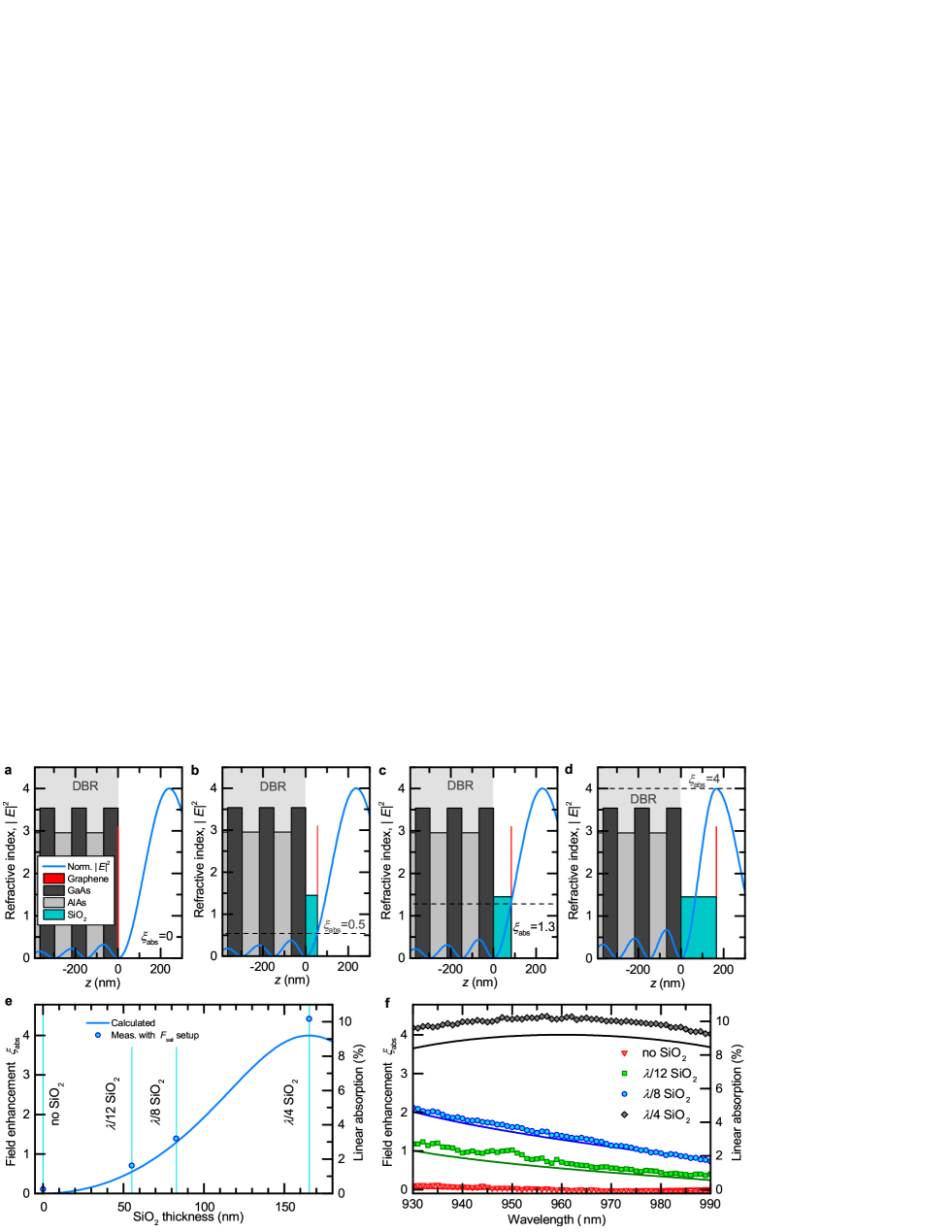
where is the wavelength, is the refractive index of air. Therefore, the SLG absorption can be tuned by changing the optical distance between SLG and the mirror surface. The SLG absorption (A) becomes , where is the absorption of a suspended and undoped SLGNair_s_08 , and is the field intensity enhancement at the absorber position. E.g., placing a SLG directly onto the mirror surface (nm) we get , thus expect no absorption, due to destructive interference between incoming and reflected waves. If SLG is placed at a distance, where there is a peak of the standing wave, we have , . Thus its absorption will increase to 400% (i.e. 4) due to constructive interference.
To verify this principle, we fabricate four GSAMs with different optical distances by coating the mirror with: 0, /12 SiO2, /8 SiO2 and /4 SiO2. We use anti-resonant distributed Bragg reflectors (DBRs)Renk_book ; Spuhler_apb_05 as high-reflection mirrors. These typically consist of a stack of multiple layers with alternating high and low refractive indexRenk_book ; Spuhler_apb_05 , each with an optical thickness of a quarter of the design wavelength. The partial reflections at the layer interfaces can interfere constructively resulting in high reflection (Renk_book ; Spuhler_apb_05 ). Our DBRs consist of 30 layer pairs of AlAs and GaAs (as described in Methods). They are designed to give a node of the standing wave at the surface of the top layer (anti-resonance), with reflectivity>99.997% at 960nm (our VECSELs wavelength). Figs.1(a-d) plot schematics of the DBR. The DBRs are then coated by plasma enhanced chemical vapor deposited SiO2 with different thickness (): 0, /12, /8 and /4, i.e 0, 55, 83, 165nm. The field intensity enhancement at the top surfaces of these devices can be calculated as (see Methods):
| (3) |
where and are the refractive index and the thickness of the SiO2 spacers at the operation wavelength . This gives a field intensity enhancement of 0, 0.5, 1.3 and 4 respectively.
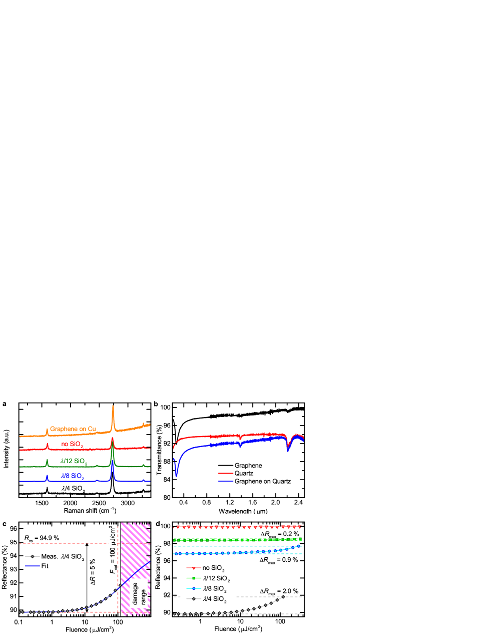
SLG is then grown by chemical vapor deposition (CVD)Bonaccorso_mt_12 ; Bae_nn_10 and transferred on top of the DBRs with SiO2-coating as described in Methods. The quality of graphene before and after transfer is monitored by Raman spectroscopyFerrari_prl_06 ; Cancado_nl_2011 ; Ferrari_nn_13 . The Raman spectrum before transfer is shown in Fig.2(a). This is measured at 457nm excitation, since this wavelength suppresses the Cu luminescence, which would result in a non-flat backgroundLag_apl_13 . The spectrum shows a very small I(D)/I(G)0.004, indicating negligible defectsFerrari_prl_06 ; Cancado_nl_2011 ; Ferrari_nn_13 ; Ferrari_prb_00 . The 2D peak is a single sharp Lorentzian with full width at half maximum, FWHM(2D)35cm-1, a signature of SLG Ferrari_prl_06 . Representative Raman spectra of the transferred graphene on the 0, /4 SiO2, /8 SiO2, /12 SiO2 devices are shown in Fig.2(a). After transfer, the 2D peak is still a single sharp Lorentzian with FWHM(2D)35cm-1, confirming that SLG has indeed been successfully transferred, and I(D)/I(G)0.005, showing that negligible additional defects are induced by the transfer process. In order to estimate the doping level of the transferred films, an analysis of more than 10 measurements is carried out for 514nm excitation. We use this wavelength as most previous literature and correlations were derived at 514nmDas_nn_08 . For the film transferred on the /8 SiO2 sample, the average G peak position, Pos(G), and FWHM(G), are 1591.8cm-1 and 14.6cm-1. The average Pos(2D) is 2693cm-1, and the 2D to G intensity and area ratios I(2D)/I(G); A(2D)/A(G), are 2.7 and 6.3. This indicates a p-doping0.51013cm-2, corresponding to a Fermi level shift300meVDas_nn_08 . Similarly, for the /4- and /12-mirrors we get a p-dopingcm-2, corresponding to a Fermi level shift<400meV. For comparison, we also transferred SLG on quartz, Fig.2(b). The band at0.270m is a signature of the van Hove singularity in the graphene density of stateskravets_prb_2010 , while those at1.4, 2.2m are due to the quartz substrate Lag_apl_13 . The absorption at 960nm (our operation wavelength) is, but it decreases to 1% at 2m due to dopingMak_prl_08 ; Lag_apl_13 . By fitting to the measured transmittance (), we get meV, consistent with the Raman estimates. However, such doping level is not enough to significantly affect the absorption at 960nm, which is measured to be (Fig.2(b)), as for intrinsic SLGNair_s_08 ; Mak_prl_08 .
The linear unsaturated absorption of our four GSAMs at 960nm, measured with a high-precision (0.05% resolution) reflectivity setupMaas_oe_08 is plotted in Fig.1(e). This also plots the calculated absorption from Eq.3. Our devices have A=0.25%, 1.6%, 3.2% and 10% at 960nm respectively, in agreement with calculations. Fig.1(f) plots the field intensity enhancement calculated from Eq.3 as a function of wavelength, compared to experiments. This further validates the results. Note that the absorption is not flat as that of graphene on quartz (Fig.2(b)), because depends on wavelength (Fig.1(f)) according to Eq.3.
We also characterize the GSAMs reflectivity as a function of input light fluence (J/cm2). The fluence-dependent reflectivity measurements (non-linear reflectivity) show an increase in reflectivity with fluence as expected from a SA, Fig.2(d). The maximum changes in reflectivity for the /12, /8 and /4 devices are 0.2%,0.9% and 2%, respectively. The measurement for the /4 SiO2 device (i.e. the sample with =4 at the graphene position) is shown in Fig.2(c). For a fast SA (i.e. where the absorber recovery time is faster than the probe pulse duration), the reflectivity can be written asLee_apb_2012 :
| (4) |
where is the unsaturated reflectivity, the non-saturable reflectivity, the saturation fluence. We estimate a saturation fluence 100J/cm2 (corresponding to a peak intensity 1.0GW/cm2), as extracted by fitting Eq.4 to the data in Fig.2(c). The estimated modulation depth is, 2.7 times larger than that reported for SLG on quartzBaek_ape_2012 . When a higher input fluence (>120J/cm2 (4GW/cm2)) is used, the GSAM reflectivity starts to increase permanently, indicating degradation. From Eq.4, of the /8 sample is estimated as200J/cm2, higher than the /4 sample, because the smaller field intensity enhancement at the absorber makes the device saturate at a higher fluence. In this case, degradation also starts at higher fluence (>300J/cm2). In SLG, the non-equilibrium (non-thermal) distribution of electrons in conduction band and holes in valence band created by an ultrafast pulse relaxes, eventually reaching thermal equilibrium with the lattice, due to various processesBrida_nc_13 ; Tomadin_prb_13 , including carrier-carrier and carrier-phonon scattering, as well as radiative electron-hole recombination (non-linear photoluminescenceLiu ; heinz ; Bonaccorso_np_10 ). In the sub-ps time-frame two main processes occur: first, the initial peak produced by the pump laser broadens, due to carrier-carrier collisions, converging towards a hot Fermi-Dirac shape on an ultrashort time scale<100fsBrida_nc_13 ; Tomadin_prb_13 . On a longer timescale, optical phonon emissionlazzeri drives a cooling in which the Fermi Dirac distribution shifts towards the Dirac pointmalic12 ; Brida_nc_13 ; Tomadin_prb_13 .
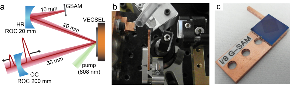
For VECSEL mode-locking we select the /8 GSAM because it offers suitable linear loss (3%). This device also provides a larger modulation depth () compared to the /12 GSAM. The laser cavity configuration is sketched in Fig.3(a), with a picture in Fig.3(b). The resonator mode and pump spot radius on the gain chip are 150m. In order to achieve a sufficient intensity to saturate the GSAM, we implement a beam waist30m on the absorber using a concave folding mirror with a 20mm radius of curvature. A picture of the /8-GSAM is shown in Fig.3(c).
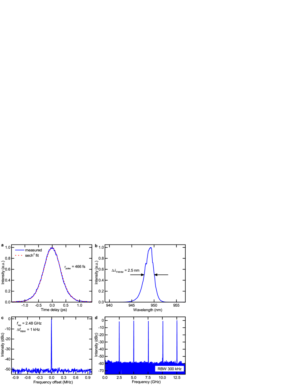
We obtain stable mode-locking with a pulse duration of 466fs (Fig.4(a)). The spectrum is centered at949nm with FWHM=2.5nm, Fig.4(b). Note that the field intensity enhancement of our /8 GSAM is =1.5 at 949nm (compared to 1.3 at 960nm, Fig.1(f)). The pulse repetition rate is 2.5GHz, detected with a fast photodiode and measured with a microwave spectrum analyzer, see Fig.4(c,d), one order of magnitude higher than previous fiberSun_an_10 ; Sun_pe_12 and solid-stateLag_apl_13 ; Sun_pe_12 lasers mode-locked by graphene, due to the compactness of our VECSEL design. The time-bandwidth product is 0.353, 1.1 times larger than what expected for transform-limited sech2 pulses, indicating that the output pulses are slightly chirped (i.e. the instantaneous frequencies are time-dependentSaleh_book ). The average output power is 12.5mW, with a 0.2% output coupling transmission. Higher power up to 26mW with 2ps pulses is also achieved using a 0.5% OC transmission. We calculate the input pulse fluence on the GSAM as125J/cm2, corresponding to a reflectivity modulation0.55%, according to Fig.2(a).
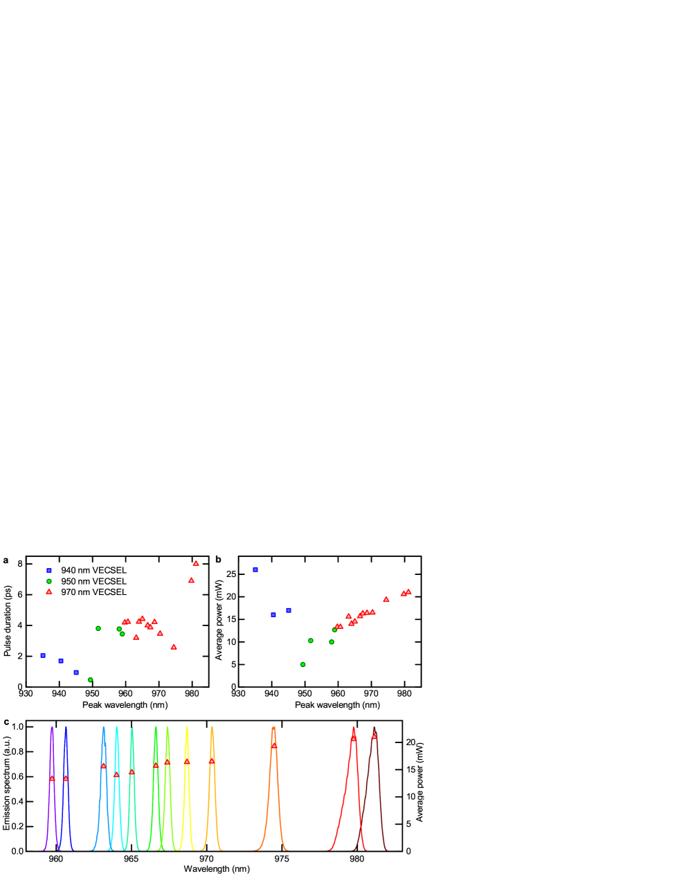
In order to verify the broadband operation of our GSAM, we also perform a wavelength-tuning study using the VECSEL described above and an additional quantum-well (QW) VECSEL optimized for emission at970nm. We use a10cm cavity at 1.5GHz, with various OC transmission rates and gain chips to fully test our GSAMs. A Fabry-Pérot fused silica etalon (20m thick) is used for wavelength tuning. In order to optimize the output power at a given emission wavelength, the gain chip heat sink temperature is adjusted between -20 and +20oC. Mode-locked operation is obtained in a range from 935 to 981nm (46nm), with pulse durations up to 8ps (Fig.5(d)). Figs.5(a,b) show the pulse duration and average output power for different emission wavelengths. A maximum tuning range of 21nm with a single VECSEL gain chip is achieved with the 970nm QW VECSEL, Fig.5(c). This is larger than previously reported with any SESAM mode-locked VECSELMorris_pw_12 .
In conclusion, we demonstrated a versatile approach to engineer the absorption of graphene saturable absorber mirrors in the 0-10% range. Accordingly, the saturation fluence can be adjusted with the field intensity enhancement. We mode-locked VECSELs with a series of different gain chips in a wavelength range as broad as 46nm (from 935 to 981nm) with repetition rate up to 2.48GHz and 466fs pulse duration. This can lead to novel graphene based ultrafast light sources to meet the wavelength range, repetition rate and pulse duration requirements for various applications (e.g. metrology, spectroscopy and data-communication).
Methods
Mirror preparation
30-pair anti-resonant AlAs/GaAs (81.1nm/67.85nm) DBRs are grown on 600m thick GaAs by molecular beam epitaxy (MBE, VEECO GEN III). Subsequently, the wafer is cleaved into 11 cm2 pieces and different SiO2 coatings are deposited using a plasma enhanced chemical vapor deposition reactor (Oxford Instruments PECVD 80+). The layer thickness is measured on reference Si samples with an ellipsometer (SENTECH SE850).
GSAM preparation
SLG is grown by CVDBae_nn_10 by heating a 35m thick Cu foil to 1000oC in a quartz tube, with 10sccm H2 flow at510-2 Torr. The H2 flow is maintained for 30min in order to reduce the oxidized Cu surfaceBonaccorso_mt_12 ; Bae_nn_10 and to increase the graphene grain sizeBonaccorso_mt_12 ; Bae_nn_10 . The precursor gas, a H2:CH4 mixture with flow ratio 10:15, is injected at a pressure of 4.510-1 Torr for 30min. The carbon atoms adsorb onto the Cu surface and form SLG via grain propagationBonaccorso_mt_12 ; Bae_nn_10 . The quality and number of graphene layers are investigated by Raman spectroscopy (Renishaw InVia micro-Raman spectrometer equipped with a Leica DM LM microscope and a 100X objective)Ferrari_prl_06 ; Cancado_nl_2011 ; Ferrari_nn_13 . A 55mm2 SLG is transferred onto the mirrors as followsLag_apl_13 ; Bonaccorso_mt_12 : First, a layer of poly(methyl meth-acrylate) (PMMA) is spin-coated on the samples. The Cu foil is etched using a mixture of 3% H2O2: 35% HCl (3:1 ratio), which is further diluted in equal volume of deionized water. The PMMA/graphene films are then rinsed in two consecutive deionized H2O baths. Next, the films are picked up on the mirror substrates and left to dry under ambient conditions. Finally, the PMMA is dissolved in acetone, leaving the SLG films on the mirrors. The transferred SLG is inspected by optical microscopy, Raman spectroscopy, and absorption spectroscopy. The non-linear reflectivity of the GSAMs is measured using the high-precision reflectivity setup described in Ref.Maas_oe_08 . A Kerr-lens mode-locked Ti:Sapphire laser (Tsunami, Spectra-Physics) is used as a probe laser, with 100fs pulse duration at a 80MHz repetition rate, with740mW average power at 960nm.
VECSEL laser and characterization
QW VECSELs emitting at940 and 970nm are grown by metal-organic vapor phase epitaxy (MOVPE, AIXTRON AIX 200/4) as for Ref.Lorenser_apb_04 . A QD VECSEL with an emission wavelength950nm is grown by MBE as described in Ref.Hoffmann_oe_11 . Instead of 9 QD layers placed in 7 subsequent anti-nodes of the electric field as in Ref.Lorenser_apb_04 , the gain chip we use here has 2 QD layers placed in the first anti-node, whereas no QDs are placed in the 6 anti-node to balance the stronger excitation due to higher absorption of the pump light around the first anti-nodes. All gain structures are grown in reverse order, and subsequently processed on a diamond heat sink grown by CVD, purchased from Diamond Materials GmbH, as described in Ref.Haring_jqe_02 . The pump laser is coupled into a 200m fiber. The laser output is characterized using a RF spectrum analyzer (HP8592L, Agilent 8565EC) and a fast photodiode (New Focus 1434). An optical spectrum analyzer (HP 70952) is used to detect the optical spectrum. The pulse train is temporally characterized with an intensity autocorrelator (Femtochrome FR103XL).
Field intensity enhancement
The absorption of a graphene layer on the top of a mirror is defined by the field intensity enhancement at the absorber position. This is determined by the constructive and destructive interference of the electric field of the incident and reflected beam. To calculate the field intensity enhancement, we assume an incident optical wave:
| (5) |
where is the wave number in the material, n is the refractive index of the material in which the light is propagating. The reflected optical wave is , because of total reflection at the mirror, the node at the surface of the mirror and the propagation in the opposite direction. From Eq.1, we get the field enhancement for an anti-resonant high-reflection mirror with no additional coating in air:
| (6) |
Then we consider the field enhancement of an anti-resonant high-reflection mirror with a SiO2-coating of thickness . At the air-SiO2-interface we haveSaleh_book :
| (7) |
where and are the Fresnel coefficientsSaleh_book of reflection at normal incidence at the air-SiO2 and SiO2-air interface. The corresponding Fresnel coefficientsSaleh_book for transmission at the air-SiO2 and SiO2-air interface are:
| (8) |
The electric field of the reflected beam consists of the superposition of the incoming beam () reflected at the air-SiO2 interface, and the electric field of the beam () transmitted in SiO2 at the same interface:
| (9) |
whereas the electric field of the incident beam in SiO2 at the interface is:
| (10) |
and the electric field of the reflected beam in SiO2 at the interface is:
| (11) |
From Eqs.10,11 we get with normalization of the incoming field ():
| (12) |
and
| (13) |
Inserting Eq.13 in Eq.9 we get the electric field of the reflected beam in air:
| (14) |
inserting Eqs.14,7,8 in Eq.1 we get:
| (15) |
which gives:
| (16) |
Acknowledgments
We thank Prof. T. Südmeyer for useful discussions. We acknowledge funding from the Royal Society, the European Research Council Grant NANOPOTS, EU grants RODIN, GENIUS, MEM4WIN, CareRAMM, and Graphene Flagship (contract no. NECT-ICT-604391), EPSRC grants EP/K01711X/1,EP/K017144/1, EP/G042357/1, Nokia Research Centre, Emmanuel College, Cambridge, the FIRST clean room facility of ETH and the Swiss National Science Foundation (SNSF).
References
- (1) Keller, U., Recent developments in compact ultrafast lasers. Nature 424, 831-838 (2003).
- (2) Keller, U. & Tropper, A. C., Passively modelocked surface-emitting semiconductor lasers. Phys. Rep. 429, 67-120 (2006).
- (3) Fermann, M.E., A. Galvanauskas, & G. Sucha, Ultrafast lasers: technology and applications (CRC Press, 2003).
- (4) Okhotnikov,O. G., Semiconductor Disk Lasers: Physics and Technology (Wiley-VCH,2010).
- (5) Aviles-Espinosa, R. et al., Compact ultrafast semiconductor disk laser: targeting GFP based nonlinear applications in living organisms. Biomed. Opt. Express 2, 739-747 (2011).
- (6) Wilcox, K. G. et al., 4.35 kW peak power femtosecond pulse mode-locked VECSEL for supercontinuum generation. Opt. Express 21, 1599-1605 (2013).
- (7) Jewell, J.L., et al., Vertical-cavity surface-emitting lasers: Design, growth, fabrication, characterization. IEEE J. of Quantum Electron. 27(6), 1332-1346 (1991).
- (8) Lorenser, D., et al., 50-GHz passively mode-locked surface-emitting semiconductor laser with 100 mW average output power. IEEE J. Quantum Electron. 42(8), 838-847 (2006).
- (9) Wittwer, V. J. et al., Timing Jitter Characterization of a Free-Running SESAM Mode-locked VECSEL. IEEE Photonics Journal 3, 658-664 (2011).
- (10) Rudin, B. et al., High-power MIXSEL: an integrated ultrafast semiconductor laser with 6.4 W average power. Opt. Express 18, 27582-27588 (2010).
- (11) Heinen, B. et al., 106 W continuous-wave output power from vertical-external-cavity surface-emitting laser, Electron. Lett. 48, pp. 516-517, 26 (2012)
- (12) Scheller, M.et al., Passively modelocked VECSEL emitting 682 fs pulses with 5.1W of average output power. Electron. Lett. 48(10), pp. 588-589, (2012).
- (13) Saraceno, C. J. et al., SESAMs for High-Power Oscillators: Design Guidelines and Damage Thresholds. IEEE J. Sel. Top. Quantum Electron. 18, 29-41(2012).
- (14) Morris, O. J. et al. in Photonics West. 824212 (SPIE,2012).
- (15) Hoffmann, M. et al., Femtosecond high-power quantum dot vertical external cavity surface emitting laser. Opt. Express 19, 8108-8116 (2011).
- (16) Bonaccorso, F., Sun, Z., Hasan, T. & Ferrari, A. C., Graphene Photonics and Optoelectronics. Nat. Photonics 4, 611 - 622 (2010).
- (17) Brida, D. et al., Ultrafast collinear scattering and carrier multiplication in graphene. Nature Comm. 4, 1987 (2013).
- (18) A. Tomadin, A. et al., Non-equilibrium dynamics of photo-excited electrons in graphene: collinear scattering, Auger processes, and the impact of screening. Phys. Rev. B 88, 035430 (2013).
- (19) Bonaccorso, F. et al., Production and processing of graphene and 2d crystals. Mater. Today 15, 564-589 (2012).
- (20) Sun, Z., Hasan, T., & Ferrari, A. C., Ultrafast lasers mode-locked by nanotubes and graphene, Physica E 44, 1082 (2012).
- (21) Hasan, T. et al., Nanotube-Polymer Composites for Ultrafast Photonics. Adv. Mater. 21, 3874-3899 (2009).
- (22) Sun, Z. et al., Graphene Mode-Locked Ultrafast Laser. ACS Nano 4, 803-810 (2010).
- (23) Nair, R. R. et al., Fine Structure Constant Defines Visual Transparency of Graphene. Science 320, 1308-1308 (2008).
- (24) Mak, K. F. et al., Measurement of the Optical Conductivity of Graphene. Phys. Rev. Lett. 101, 196405 (2008).
- (25) Baek, I. H. et al., Efficient Mode-Locking of Sub-70-fs Ti:Sapphire Laser by Graphene Saturable Absorber. Appl. Phys. Express 5, 032701 (2012).
- (26) Lagatsky, A. A. et al., 2m Solid-State Laser Mode-locked By Single-Layer Graphene. Appl. Phys. Lett. 102, 013113 (2013).
- (27) Mary, R. et al., 1.5 GHz picosecond pulse generation from a monolithic waveguide laser with a graphene-film saturable output coupler, Opt. Express 21, 7943 (2013).
- (28) Mangold, M. et al., VECSEL gain characterization, Opt. Express 20, 4136 (2012).
- (29) Lee, C. C., Miller, J. & Schibli, T., Doping-induced changes in the saturable absorption of monolayer graphene. Appl. Phys. B 108, 129-135 (2012).
- (30) Wang, F. et al., Gate-variable optical transitions in graphene,Science 320, 206 (2008).
- (31) Spuhler, G. J. et al., Semiconductor saturable absorber mirror structures with low saturation fluence. Appl. Phys. B 81, 27-32 (2005).
- (32) Renk, K.F., Basics of laser physics (Springer, 2012).
- (33) Bae, S. et al., Roll-to-roll production of 30-inch graphene films for transparent electrodes. Nat. Nanotechnol. 5, 574 - 578 (2010).
- (34) Ferrari, A. C. et al., Raman Spectrum of Graphene and Graphene Layers. Phys. Rev. Lett. 97, 187401 (2006).
- (35) Cancado, L. G. et al., Quantifying Defects in Graphene via Raman Spectroscopy at Different Excitation Energies. Nano Lett. 11, 3190-3196 (2011).
- (36) Ferrari, A. C. & Basko,D. M., Raman spectroscopy as a versatile tool for studying the properties of graphene, Nat. Nanotechnol. 8, 235 (2013).
- (37) Ferrari, A. C. & Robertson, J., Interpretation of Raman spectra of disordered and amorphous carbon. Phys. Rev. B 61, 14095-14107 (2000).
- (38) Das, A. et al., Monitoring dopants by Raman scattering in an electrochemically top-gated graphene transistor, Nat. Nanotechnol. 3, 210 (2008).
- (39) Kravets, V. G. et al., Spectroscopic ellipsometry of graphene and an exciton-shifted van Hove peak in absorption, Phys. Rev. B 81, 155413 (2010).
- (40) Maas, D. J. et al., High precision optical characterization of semiconductor saturable absorber mirrors. Opt. Express 16, 7571-7579 (2008).
- (41) Casiraghi, C. et al., Rayleigh Imaging of Graphene and Graphene Layers. Nano Letters, 7(9), 2711-2717 (2007).
- (42) Liu, W.-T. et al., Nonlinear broadband photoluminescence of graphene induced by femtosecond laser irradiation Phys. Rev. B, 82, 081408 (2010).
- (43) Lui, C. H. et al., Ultrafast Photoluminescence from Graphene, Phys. Rev. Lett. 105, 127404 (2010).
- (44) Lazzeri, M. et al., Electron Transport and Hot Phonons in Carbon Nanotubes, Phys. Rev. Lett. 95 236802 (2005).
- (45) Malic, E., Winzer, T. & Knorr, A., Efficient orientational carrier relaxation in optically excited graphene, Appl. Phys. Lett. 101, 213110 (2012).
- (46) Saleh, B.E.A. & Teich, M.C., Fundamentals of Photonics. (John Wiley & Sons, Inc., 1991).
- (47) Lorenser, D. et al., Towards Wafer-Scale Integration of High Repetition Rate Passively Mode-Locked Surface-Emitting Semiconductor Lasers. Appl. Phys. B 79, 927-932 (2004).
- (48) Haring, R. et al., High-power passively mode-Clocked semiconductor lasers. IEEE J. Quantum Electron. 38, 1268-1275 (2002).