Dimensionality driven charge density wave instability in TiS2
Abstract
Density functional theory and density functional perturbation theory are used to investigate the electronic and vibrational properties of TiS2. Within the local density approximation the material is a semi-metal both in the bulk and in the monolayer form. Most interestingly we observe a Kohn anomaly in the bulk phonon dispersion, which turns into a charge density wave instability when TiS2 is thinned to less than four monolayers. Such charge density wave phase can be tuned by compressive strain, which appears to be the control parameter of the instability.
Introduction. Titanium disulfide (TiS2), a prototypical layered transition metal dichalcogenide (LTMD), consists of covalently bonded Ti and S atoms arranged in two-dimensional hexagonal planes (monolayers). In the bulk form monolayers are stacked together by weak van der Waals forces. Many conflicting results exist in literature on the electronic structure of bulk TiS2, namely it is still debated whether the material is metallic, semi-metallic or semiconducting. Several experimental works report TiS2 to be a semiconductor with a bandgap ranging from 0.05 to 2.5 eV. These observations are supported by angle-resolved photo-emission spectra PRB_1980_21_615 , optical absorption JPChS_1965_26_1445 , Hall JPCssp_1984_17_2713 ; JPC_1977_10_705 and transport measurements JPC_1983_16_393 . At the same time a second set of experiments places TiS2 among metals and semi-metals with an indirect bandgap overlap ranging from 0.2 to 1.5 eV (between the and the L point in the Brillouin zone). This experimental evidence is based on extensive resistivity measurements PRL_1972_29_163 , infrared reflectance PRB_1973_7_3859 and X-ray emission and absorption PRB_1973_8_3576 .
TiS2 has drawn considerable attention over the past four decades because of the variety of its potential applications. For instance, alkali atoms and organic molecules can be intercalated easily into TiS2 for applications related to both light-weight and high-energy-density batteries AdvP_1987_36_1 ; Sc_1976_192_1126 . In particular, it has been demonstrated that for bulk TiS2 the intercalation changes the conductivity AdvP_1989_38_565 . A second interesting aspect is that both the electronic structure and the electron transport properties of TiS2 can be modulated by external pressure. Many experimental JPCssp_1984_17_2713 ; JAP_2011_109_053717 as well as theoretical JPCssp_1985_18_1595 ; JPCM_2011_23_055401 ; SSSc_2010_12_1786 studies describe pressure induced phase transitions in TiS2. For instance, the transition from a semiconductor to a semi-metal phase has been supported by Hall measurements on TiS2 single crystals under a 4 GPa pressure JPCssp_1984_17_2713 . Such evidence highlights the strong coupling between the electronic properties and the TiS2 structure, a feature shared by many LTMDs.
In fact, the LTMD family in general exhibits strong electron-phonon coupling AdvP_1987_36_1 . Often this results into ground states displaying a macroscopic order. For instance bulk NbSe2 and TaSe2 are notoriously known to exist in both a superconducting and a charge-density wave (CDW) state NJP_2008_10_125027 . Recently a significant experimental effort has been devoted to produce ultra-thin layers of such class of materials either by synthesis NatNano_2012_7_699 or by exfoliation JCScience . The appeal of reduced dimension LTMDs is that their electronic and vibrational properties are strongly modified when the thickness reduces down to ultra-thin layers, resulting in further potential for future applications. For example, photo-luminescence emerges due to an indirect to direct bandgap change when the thickness of MoS2 is reduced from bulk to monolayer NL_2010_10_1271 . In contrast, the TiSe2 phonon spectrum softens with decreasing the layers thickness NL_2012_12_5941 .
In this work, we study the changes in the electronic and vibrational properties of the TiS2, when the material is thinned from bulk to the monolayer limit. In particular we demonstrate that, if the material is metallic, a CDW phase will emerge when the number of layers is reduced below four. Intriguingly the phase transition can be driven by compressive strain.
Methodology. The electronic and vibrational properties of bulk and monolayer TiS2 have been investigated by using respectively ab-initio density functional theory PR_136_B864 ; PR_140_A1133 and density functional perturbation theory RMP_73_515 . We have considered the local density approximation (LDA) PRL_1980_45 of the exchange and correlation functional, as implemented in the Quantum Espresso package QE , except for a set of calculations (see later) where the LDA+ schemeLDAU , still within Quantum Espresso, has been employed. Ultra-soft pseudo-potentials describe the core electrons of all the atomic species. The electronic wavefunction is expanded using plane waves up to a cutoff energy of 70 Ry. Calculations for bulk TiS2 are performed for a periodic structure with the P1 space group. In contrast, for TiS2 monolayers a 12 Å vacuum region is inserted along the non-periodic direction (-axis). Geometries are relaxed by conjugate gradient, where both the atomic positions and the cell parameters are allowed to relax until the forces on each atom are less than 0.005 eV/Å. The electronic integrations are carried out by using a 161610 (20201) Monkhorst-Pack -grid for bulk (monolayer) TiS2 and a Hermite Gaussian smearing of 0.01 Ry is used for all the calculations. In computing the phonon spectrum the dynamical matrix is evaluated over a 442 (441) phonon-momentum grid and it is interpolated throughout the Brillouin zone in order to plot the bulk (monolayer) phonon bandstructure.
Results and discussion. We begin by calculating the electronic properties of bulk TiS2. The optimized bulk cell parameters are Å, Å, in good agreement with the previous theoretical (LDA) values JPCM_2011_23_055401 of Å, Å and with the experimental ones PRB_57_5106 of Å, Å. The Ti-S bond length is found to be 2.38 Å, again in close agreement with the experimental value AdvP_1969_18_193 of 2.32 Å and with a previous theoretical (LDA) estimate SSSc_2010_12_1786 of 2.383 Å. The calculated energy bandstructure along the high symmetry lines in the bulk TiS2 (P1) Brilloiun zone is shown in Fig. 1(a). Clearly bulk TiS2 is predicted to be a semi-metal with an indirect band-overlap of 0.16 eV (negative bandgap). The valence band maximum is found to be located at the point, while the conduction band minimum is at L. The corresponding partial density of states (DOS) projected over the different atomic species shows that the valence and the conduction band originate respectively from the S 3 and the Ti 3 orbitals, although there is a good degree of hybridization, see Fig. 1(b). This is in good agreement with previous calculations JAP_2011_109_053717 .
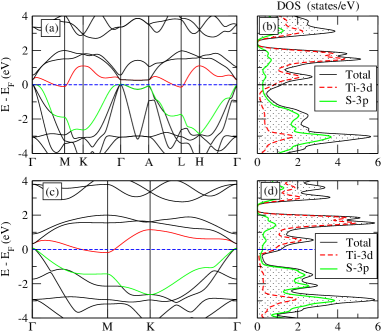
Next we move to study the electronic properties of TiS2 in its monolayer form [see figures 1(c) and 1(d)]. Our optimized lattice constant, , is now 3.32 Å. Such value slightly underestimates the experimentally observed one ACIE_2011_50_11093 of 3.40 Å, as expected from the covalent nature of the Ti-S bond and the general tendency of the LDA to overbind. Our calculations show that the electronic property, i.e. the bandgap, does not change significantly when the thickness decreases from bulk to a single monolayer. Our computed LDA negative bandgap of -0.25 eV is in good agreement with the previous theoretical calculations JPCC_116_8983 . Also in TiS2 monolayers, like in the bulk, the conduction and valence bands are respectively derived from Ti and S orbitals [Fig. 1(d)].
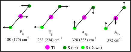
We now investigate the effects of the dimensionality on the phonon properties of TiS2 by starting from its bulk form, whose phonon dispersion is plotted in Fig. 2(a) along the -M-K--A -path. In order to facilitate a comparison with experiments we recall that the irreducible representation of the zone-center phonon modes reads
| (1) |
where R and IR denote respectively Raman and infrared active modes. The corresponding atomic displacements of the optical modes at the -point are shown in Fig. 3. Notably the phonon frequencies of a number of modes have been measured experimentally by vibrational spectroscopy, such as Raman, infrared and neutron scattering PRB_1992_45_14347 ; PRB_1986_33_4317 . These values are also reported in Fig. 3, demonstrating a good agreement with our calculated ones. In addition, our phonon dispersion agrees quite well with previous theoretical calculations based either on empirical-valence-force-field methods PRB_1992_45_14347 or on state of the art first principle density functional perturbation theory JPCM_2011_23_055401 . Interestingly, we observe the signature of a soft-phonon mode, generally called Kohn anomaly, at the M point in the Brillouin zone. This signals an incipient structural instability, which is yet not fully realized in the bulk.
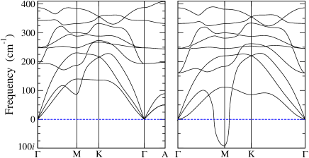
The phonon dispersion of TiS2 in the monolayer form is shown in Fig. 2(b). Similarly to the bulk phonon dispersion also for the monolayer there is no energy-gap between the optical and the acoustic phonon modes. However, we find that when TiS2 is thinned down to a monolayer the Kohn instability at M becomes a dynamically instability, namely there is now an imaginary phonon frequency at M. This reflects the fact that the system gets stabilized by forming a 22 superstructure, i.e. a commensurate CDW phase where the atomic positions are distorted. If one now constructs a 22 supercell such an instability migrates at the point, reflecting the fact that M folds to in the supercell. Now atomic relaxation of the supercell gives us a new distorted structure, which is 1.1 meV/formula-unit lower in energy than the undistorted one. The phonon bandstructure for such new distorted phase has now only real frequencies, indicating that no further symmetry lowering is present. A schematic diagram of the distorted superstructure is shown in Fig. 4(b). The direction of the distortion of the atomic positions are determined by the -vector, at which the unstable phonon mode occurs. In such new CDW phase the displacement of the Ti atoms, is much larger, 0.05 Å, than that of S 0.005 Å.
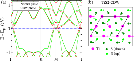
The bandstructure for the monolayer as calculated for the 22 supercell is presented in Fig. 4(a) for both the normal and the CDW phase. The crucial aspect is that in the CDW phase the material is able to open a bandgap of 0.09 eV, i.e., as expected, the emergence of the CDW phase is associated to a metal to insulator transition. The microscopic origin of the CDW phase is mainly associated to the strong electron-phonon coupling in LTMDs, which allows one to modify significantly the bandstructure with moderate lattice distortions. This is a feature common to the entire class of LTMD materials JPSJ_1994_63_156 ; PRL_1975_32_117 . A similar CDW phase transition has been observed experimentally in bulk TiSe2, a compound iso-structural to TiS2, and the transition temperature was reported to be as large as 200 K NL_2012_12_5941 .
Intriguingly, we find that the formation of the CDW phase is not a unique feature of the TiS2 monolayer. In fact, we have repeated the phonon calculation for the TiS2 unit cell and a number of layers ranging from one to four and found imaginary phonon frequencies in all cases. In particular we report frequencies of -92 cm-1, -52 cm-1, -18 cm-1 and -21 cm-1, respectively for one, two, three and four layers (note that here we report the purely imaginary part of the frequency). Considering that our accuracy over the frequency is of the order of 20 cm-1, we can conclude that the CDW phase is certainly present for both mono- and bi-layers and it vanishes for structures containing between three and four layers. This indicates that the interlayer interaction plays an important role in determining the condition for the CDW instability.
Another possibility for suppressing the CDW phase is by applying isotropic pressure, as already suggested for bulk TiSe2 PRL_2011_106_196406 . This can be simulated by performing phonon bandstructure calculations for isotropically compressed unit cells and here we report results for the monolayer case. Importantly such compression does not alter significantly the electronic structure, and the material remains metallic at all the pressures investigated with the only notable effect being an increase of the S- bandwidth as the pressure gets larger. The situation, however, is different for the phonon bandstructure. As a demonstration in Fig. 5(a) we present data for a compressive strain of 6.6%. Interestingly, the minimum frequency of the soft-phonon mode at the M point has an imaginary value (-8 cm-1) significantly smaller than the case when no pressure is applied (-92 cm-1). Consequently, the energy gain due to the CDW formation reduces with increasing the compressive strain. Eventually, the unstable mode disappears for a compressive strain of 7.1%, which corresponds to a hydro-static pressure of 3.9 GPa. Such disappearance of the CDW can be explained by considering how the inter-atomic force constants change under compressive strain. Increasing the pressure causes the Ti-S bond length to decrease and enhances the stiffness of the nearest neighbors Ti-S force constant. As a consequence the energy of the soft-phonon mode increases and eventually the instability is removed. As such the CDW instability is sensitive on the local environment around the transition metal atoms in the TiS2 layer.
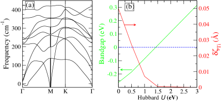
As mentioned before and demonstrated in Fig. 4 the formation of the CDW is associated to a metal to insulator transition. One then expects the CDW phase to emerge only in materials that are either metals or small-bandgap semiconductors in their undistorted geometry. The case of TiS2 is somehow unclear since there exists significant ambiguity on the experimental determination of the bandgap (or its absence). From the theoretical point of view it is important to mention that the LDA systematically underestimates the bandgap, so that the calculated semi-metal ground state might not correspond to the correct one. To complicate the comparison with experiments there is also the fact that in LTMD monolayers the exciton binding energy can be as large as 1 eV, meaning that the quasi-particle and the optical gap may differ significantly from each other PRB_86_241201 . As such it is useful to revisit our results this time by using an exchange and correlation functional, which allows us to systematically open a bandgap in the undistorted phase. Considering the predominant 3 character of the valence band, the LDA+ functional LDAU appears to be an ideal choice, since the Coulomb repulsion parameter, can be used a control parameter for the opening of the gap.
In Fig.5(b) we report our results showing the variation of the bandgap of the undistorted phase and the Ti displacement, , as a function of . Clearly we observe that the lattice distortion vanishes as soon as is large enough to open a bandgap in the undistorted phase. In other words the metallicity on the undistorted phase is a necessary condition for the emerge of the CDW ground state. At this point we are not in the position to make a final judgment on the metallicity of TiS2, however our results show convincingly that the electron phonon coupling in TiS2 is strong enough to drive a CDW instability as long as the material is metallic. This means that, even if pristine TiS2 is a small-gap insulator, small doping levels (e.g. by intercalating alkali atoms) will be sufficient to trigger the instability.
Conclusion. In summary, we have performed electronic and phononic bandstructure calculations for TiS2 both in the bulk and monolayer form. In both cases the electronic structure derived from DFT-LDA is that of a semimetal with the band overlap points being different depending on the dimensionality. More interestingly we have found that, in contrast to other Ti-based chalcogenides, the bulk form of TiS2 is undistorted, while a CDW instability emerges for nanostructures made of less than four monolayers. Furthermore the CDW instability can be controlled by pressure and for the monolayer it vanishes at around 4 GPa. Since the emergence of the CDW phase depends of the metallic state of the undistorted structure we have discussed the issue of the bandgap. Our results point to a situation where the material can distort either in its pristine form or in condition of moderate doping.
Acknowledgement. This work is supported by CRANN. We thank Trinity Centre for High Performance Computing (TCHPC) for the computational resources provided.
References
- (1) C. H. Chen et al., Phys. Rev. B 21, 615 (1980).
- (2) D. L. Greenaway and R. Nitsche, J. Phys. Chem. Solids 26, 1445 (1965).
- (3) P. C. Klipstein and R. H. Friend, J . Phys. C : Solid State Phys. 17, 2713 (1984).
- (4) R.H. Friend, D. Jerome, W.Y. Liang, C. Mikkelsen and A.D. Yoffe, J. Phys. C 10, L705 (1977).
- (5) J.J. Barry, H.P. Hughes, P.C. Klipstein and R.H. Friend, J. Phys. C 16, 393 (1983).
- (6) A.H. Thompson, K.R. Pisharody and R.F. Koehler, Phys. Rev. Lett. 29, 163 (1972).
- (7) G. Lucovsky, R.M. White, J.A. Benda and J.F. Revelli, Phys. Rev. B 7, 3859 (1973).
- (8) D.W. Fischer, Phys. Rev. B 8, 3576 (1973).
- (9) R.H. Friend and A.D. Yoffe, Adv. Phys. 36, 1 (1987).
- (10) M.S. Whittingham, Science 192, 1126 (1976).
- (11) M. Inoue, H.P. Hughes and A.D. Yoffe, Adv. Phys. 38, 565 (1989).
- (12) B. Liu et al., J. Appl. Phys. 109, 053717 (2011).
- (13) Y. G. Yu and N. L. Ross, J. Phys.: Condens. Matter 23, 055401 (2011).
- (14) G. . Benesh, A.M. Woolley and C. Umrigar, J . Phys. C: Solid State Phys. 18, 1595 (1985).
- (15) F. Yu, J.-X. Sun and Y.-H. Zhou, Solid State Science 12, 1786 (2010).
- (16) D. S. Inosov et al., New J. Phys. 10, 125027 (2008).
- (17) Q. H. Wang, K. Kalantar-Zadeh, A. Kis, J. N. Coleman and M. S. Strano, Nature Nanotech. 7, 699 (2012).
- (18) V. Nicolosi, M. Chhowalla. M.G. Kanatzidis, M.S. Strano and J.N. Coleman, Science 340, 1420 (2013).
- (19) A. Splendiani et al., Nano Lett. 10, 1271 (2010).
- (20) P. Goli, J. Khan, D. Wickramaratne, R.K. Lake and A. A. Balandin, Nano Lett. 12, 5941 (2012).
- (21) P. Hohenberg and W. Kohn, Phys. Rev. 136, B864 (1964).
- (22) W. Kohn and L.J. Sham, Phys. Rev. 140, A1133 (1965).
- (23) S. Baroni, S. de Gironcoli, A. Dal Corso, and P. Giannozzi, Rev. Mod. Phys. 73, 515 (2001) .
- (24) D.M. Ceperley and B.J. Alder, Phys. Rev. Lett. 45, 566 (1980).
- (25) P. Giannozzi et al., J. Phys.: Condens. Matter 21, 395502 (2009).
- (26) A.I. Liechtenstein, V.I. Anisimov and J. Zaanen, Phys. Rev. B 52, R5467(1995).
- (27) D.R. Allan, A.A. Kelsey, S.J. Clark, R. J. Angel and G.J. Ackland, Phys. Rev. B 57, 5106 (1998)
- (28) J.A. Wilsona and A.D. Yoffe, Adv. Phys. 18, 193 (1969).
- (29) Z. Zeng et al., Angew. Chem. Int. Ed. 50, 11093 (2011).
- (30) C. Ataca, H. Şahin and S. Ciraci, J. Phys. Chem. C 116, 8983 (2012).
- (31) S.J. Sandoval, X. K. Chen and J.C. Irwin, Phys. Rev. B 45, 14347 (1992).
- (32) M. Scharli and F. Lévy, Phys. Rev. B 33, 4317 (1986).
- (33) Y. Nishio, M. Shirai, Naoshi, and K. Motizuki, J. Phys. Soc. Jap. 63, 156 (1994).
- (34) J. A. Wilson, F. J. DiSalvo and S. Mahajan, Phys. Rev. Lett. 32, 117 (1975).
- (35) M. Calandra and F. Mauri, Phys. Rev. Lett. 106, 196406 (2011).
- (36) H.-P. Komsa and A. V. Krasheninnikov, Phys. Rev. B 86, 241201(R) (2012).