Thermoelectric properties of atomic-thin silicene and germanene nano-structures
Abstract
The thermoelectric properties in one- and two-dimensional silicon and germanium structures have been investigated using first-principle density functional techniques and linear response for the thermal and electrical transport. We have considered here the two-dimensional silicene and germanene, together with nano-ribbons of different widths. For the nano-ribbons, we have also investigated the possibility of nano-structuring these systems by mixing silicon and germanium. We found that the figure of merit at room temperature of these systems is remarkably high, up to 2.5.
pacs:
73.50.Lw,63.22.-m,73.50.-hI Introduction
Thermoelectric energy conversion is the ability of a device to convert a steady temperature gradient into an electrical current, and it was firstly discovered by Seebeck in 1821.Pollock (1985); Nolas et al. (2001); Goldsmid (2010) In a reverse mode operation, a thermoelectric device can be used as a cooler by maintaining a steady current in the device (Peltier effect).Pollock (1985); Nolas et al. (2001); Goldsmid (2010) Recently, the quest for a highly efficient thermoelectric device has attracted tremendous interests due to significant potential industrial applications.Pollock (1985); DiSalvo (1999); Nolas et al. (2001); Vining (2009); Goldsmid (2010) The efficiency of the thermoelectric conversion is characterized by a dimensionless parameter, called figure of merit
| (1) |
where is the electric conductance, is the Seebeck coefficient, is the absolute temperature, is the total thermal conductance that is usually splits into the electron and phonon contributions, respectively.Pollock (1985); Nolas et al. (2001); Goldsmid (2010) Generally speaking, materials with are regarded as good thermoelectric components, while devices with a approaching to or larger than 3 could efficiently compete with conventional energy conversion techniques. State of the art values for the figure of merit are about 1, while higher values have been reported in the literature for particular materials which, however, have presently proven difficult to integrate into our technologies or to produce industrially in a reliable way, or whose cost makes them unaffordable at large scale.Venkatasubramanian et al. (2001) Admittedly, the optimization of the figure of merit is a difficult problem. Indeed, an ideal thermoelectric material should hold the electric conductance and the Seebeck coefficient as high as possible, while keeping the thermal conductance as low as possible. Unfortunately, because of the Wiedemann-Franz law (valid in a great extent for metals), where and are, respectively, the Boltzmann constant and carrier charge,Ashcroft and Mermin (1976) the two conductances are locked together and increasing the first leads to an increase in the second. It therefore looked natural to attempt to decrease the phonon thermal conductance since this will hopefully not (strongly) affect the electronic properties, although the maximum achieved so far makes these devices not commercially viable.
After the seminal work by Hicks and Dresselhaus,Hicks and Dresselhaus (1993) a strong research activity has been focused on nano-structured materials for thermoelectric applications. This boost can easily be explained as an attempt to escape from the Wiedemann-Franz law while dramatically increasing the electronic density of states.Minnich et al. (2009); Pichanusakorn and Bandaru (2010) With the discovery of graphene,Novoselov et al. (2004) and the subsequent investigation of its properties, it became apparent that graphene is not an efficient thermoelectric material since its thermal conductance is extremely high. Balandin et al. (2008); Seol et al. (2010); Prasher (2010) On the other hand, it has been shown that nano-structuring graphene with boron-nitride in a nano-ribbon increased the overall figure of merit by a factor 20.Yang et al. (2012) Notwithstanding its phenomenal properties, the integration of graphene with the actual silicon-based technologies has proven a quite challenging task, whose solution would probably require the complete redesign of electronics devices. As our present technology is based on silicon (Si) and germanium (Ge) semiconductors, it thus appears natural to look at the thermoelectric properties of these materials, since the integration of a thermoelectric device based on them would be simpler than the integration of carbon-based devices. For example, in silicon nano-wires, the thermal conductance can be reduced in a factor of 100 due to the quenching of phonon transport and they exhibit a high thermoelectric conversion ratio.Hochbaum et al. (2008) This suggests a prospective avenue to improve the thermoelectric performance through decreasing the characteristic size of materials and various nano-structures such as nano-tubes and nano-membranes can be proposed.
Silicene resembles graphene Castro Neto et al. (2009); Peres (2010); Ayala et al. (2010); Das Sarma et al. (2011); Kotov et al. (2012) in the atomic single layer arrangements, i.e., it forms a honeycomb lattice and shares with the carbon system similar electronic properties. In particular, it is viewed as new type of atomic-layered materials with outstanding properties such as the zero effective mass at the Dirac-point and infrared absorbance optical spectra.Cahangirov et al. (2009); Chen et al. (2012); Bechstedt et al. (2012) Experimentally, single layer silicene (buckled)De Padova et al. (2010); Lalmi et al. (2010); De Padova et al. (2012); Kara et al. (2012); Feng et al. (2012); Enriquez et al. (2012); Jamgotchian et al. (2012); Vogt et al. (2012); Lin et al. (2013); Chen et al. (2013); Meng et al. (2013); Cahangirov et al. (2013) and silicene nano-ribbons (SiNRs)De Padova et al. (2010, 2012) have been synthesized on Ag substrate. In particular, SiNRs up to a narrow width of 1.6 nm have been produced, aligned parallel to each other in a well-distributed way.De Padova et al. (2010) From the experience gained with the current micro-electronics, we know that Ge is a good partner for Si since they share similar electronic properties and form bulk crystal with comparable lattice constant ( nm, while nm, with a lattice mismatch of 4%). The elastic limit is around 7%. In the case of InAs, for instance, only one monolayer can be grown on GaAs.Li et al. (1994) A single layer hexagonal lattice of Ge, called germanene, has been predicted from an ab-initio calculations.Cahangirov et al. (2009) Theoretically, germanene presents a Dirac point, and the electronic and structural properties of this material would be very similar to those of silicene. We will discuss some of them in more detail in the following. In particular, we will consider germanene nano-ribbons (GeNRs) of different widths and the possibility of forming Si-Ge single atomic layered nano-ribbons by alternating stripes of Si with stripes of Ge.
In this paper, we investigate with ab-initio technique combined with linear response approach the thermoelectric properties of both two-dimensional (2D) silicene and germanene nano-sheets and one-dimensional (1D) nano-ribbons. We find that some of these systems will show a figure of merit larger than 1 at room temperature (with a maximum value of 2.18). Our results are consistent with those obtained by Pan et al.Pan et al. (2012), although they are based on different techniques especially for the calculations of the phonon thermal conductance. We believe that this agreement is partially fortuitous, as we will discuss in the following.
The paper is organized as follows. In Sec. II we will discuss in details the numerical and theoretical methods we used to investigate the Si and Ge systems. In Sec. III, we introduce the 2D systems, silicene and germanene, study their stability and investigate their transport properties. In Sec. IV, we investigate the 1D nano-ribbons. In this section we focus mostly on the Ge system, since the SiNRs have been investigated elsewhere, and from our calculations, Si and Ge nano-ribbons do share essentially some same properties. We find that the nano-ribbons can have a quite large figure of merit. This is due to the fact that both Si and Ge nano-ribbons do have a finite electronic gap that dramatically enhances the Seebeck coefficient. In Sec. V, we consider nano-ribbons created by alternating stripes of Si and Ge. By nano-structuring the nano-ribbons we would like to confine the phonons and therefore decrease the thermal conductance. However, we report that the SiGeNRs do show some the same transport properties of the pure Si or pure Ge nano-ribbons. This is due to the limitations of our method of choice, namely a full ab-initio study for the phonon energy transport. Indeed, within this technique we are limited to fairly small nano-ribbons and therefore the long-wavelength phonons are not quenched by the regular pattern of the structured nano-ribbons. On the other hand, a classical technique, based on molecular dynamics, would allow us to calculate the thermal conductance of larger devices. However, this technique does not recover the correct quantum limit of these one-dimensional systems, and therefore we do expect that the molecular dynamics results to give the incorrect thermal conductance at temperature below the Debye temperature, which for Si and Ge systems can be estimated to be about 640 K and 374 K, respectively. We check the idea that nano-structuring would decrease the phonon thermal conductance by using a tight-binding approximation, which allows us to consider larger super-cell than a purely ab-initio method. We indeed show that the thermal conductance does strongly decrease when we consider a hetero-structure of Si and Ge. Finally, in Sec. VI we draw our conclusions and some outlooks of this work.
II Method
In linear response theory, by using the Onsager’s relations and the Landauer’s theory of quantum transport, the electrical conductance , the Seebeck coefficient , and the electron contributed thermal conductance , can be written asNolas et al. (2001); Goldsmid (2010); D’Agosta (2013)
| (2) | |||
| (3) | |||
| (4) |
where
| (5) |
is the Lorenz integral. In these equations, is the chemical potential, is the area of the considered system, and are the indices of the spatial components, , and , is the Fermi distribution function at a given temperature , and is a transmission function which is related to the probability of electrons to cross the system.Landauer (1957); Baranger and Stone (1989) Similarly, the phonon thermal conductance is given byYamamoto and Watanabe (2006)
| (6) |
where is the phonon-vibrational frequency, is the reduced Planck-constant, and is the Bose-Einstein distribution function. Again, is a transmission function for phonons. A common expression of the electron and phonon transmission functions can be given in terms of the electron and phonon band structures, respectively,
| (7) |
where is the number of sampled -point in the first Brillouin-zone, is the band index, is the relaxation time of electrons/phonons, is the velocity calculated from the band dispersion, and is the electron/phonon density of states associated with the band .
To obtain the energy band structure, we perform first-principle calculations within the local density approximation by using the projector-augmented wave potentials as implemented in VASP.Kresse and Furthmüller (1996) The exchange correlation energy is chosen in the form of Ceperley-Alder which has been parameterized by Perdew and Zunger.Ceperley and Alder (1980); Perdew and Zunger (1981) For the self-consistent potential and the total energy calculations, the -points of the Brillouin-zone in the reciprocal space are sampled by a (2511) Monkhorst-Pack grids. The kinetic energy cut-off is set to 500 eV. After ionic relaxation, the Hellmann-Feynman forces acting on each atom are less than 0.01 eV/Å. We obtain the force constant matrix for the calculation of the phonon dispersion, through the small displacement method.Alfè (2009) We use a supercell technique with a 15 Å of vacuum. In these calculations we have neglected both the phonon-phonon and the electron-phonon interactions. We expect that for the low energy phonons, mostly responsible for the thermal transport, the correction due to these interactions to be small, especially for the Seebeck coefficient.
In the following, we will consider both the figure of merit of Eq. (1) and the electronic figure of merit , defined as
| (8) |
Then Eq. (1) can be rewritten as
| (9) |
Although is not a physical measurable quantity, it is useful because it provides an upper bound to the total figure of merit, and since it does not include the phonon thermal contribution is easier to calculate. A small will therefore imply a small figure of merit .
III Two-dimensional silicon and germanium crystals
We first investigate the electronic properties of a single-layer of silicon, i.e., silicene. In trying to closely reproduce the experimental setup,Vogt et al. (2012); Feng et al. (2012); Lin et al. (2013) we put one-layer of 33 silicene on top of five-layers of 44 Ag(111): according to experimental evidence, the two lattices should match, thus decreasing the total stress at the boundary and creating an ideal supercell for our calculations. The geometrical structure for silicene obtained after the full relaxation is shown in Fig. 1(a) and corresponds to the structure discussed in Ref. Cahangirov et al., 2013. We have superimposed the Ag(111) layer to show the excellent structural matching, as highlighted by the boundary continuous (red) line. Figure 1(b) shows the silicene obtained by removing the silver substrate in Fig. 1(a). Contrary to graphene, silicene is not a strict two-dimensional system, in the sense that the atoms in silicene are arranged on two atomic layers with a fairly small buckling distance, which depends on the presence of the substrate. Indeed, it is found that the atomic arrangement is further distorted by the metallic substrate.Cahangirov et al. (2013) Starting from a single layer of silicon, arranged in a plane on an hexagonal lattice without the Ag substrate, we would have obtained a system with a different buckling, where the atoms would divide equally between the upper and lower plane. In our optimized structure however, we observe that the silicene presents buckling forming two atomic layers with six atoms on top of the other twelve atoms which are therefore closer to the Ag surface. The buckling distance between these two layers is about 0.79 Å. In Fig. 1(c) the electronic energy band for the distorted silicene is plotted along the high-symmetry points of the first Brillouin-zone, where the dotted line indicates the Fermi energy that we set for convenience at 0. It can be seen that a band gap about 0.3 eV crosses the Fermi energy, indicating semiconducting properties of the system. This must be compared with the flat silicene (unoptimized structure) and the silicene optimized without the Ag substrate, which both present a Dirac point at the K point of the first Brillouin-zone, therefore both showing metallic properties (see Fig. 3). A detailed discussion of the electronic structure of supported silicene can be found in Ref. Cahangirov et al., 2013.
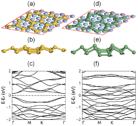
Germanene is an analog of silicene, where the silicon atoms are replaced by germanium. Although, to the best of our knowledge, up to now there is no direct experimental observation of these structures, here we study the electronic properties of two-dimensional germanene. Figure 1(d) shows the atomic structure of one-layer 33 germanene on top of five-layers 44 Ag(111), and Fig. 1(e) shows the unsupported single-layer germanene by removing the silver substrate. The structure has been fully relaxed. It is found from Fig. 1(e) that similar to silicene, two layers are formed with six Ge atoms on the top layer and the other twelve Ge atoms on the bottom layer closer to the Ag surface. The buckling distance between the two layers is about 1.42 Å. Figure 1(f) shows the band structure of the distorted germanene without the Ag substrate. It is found that there is no gap through the Fermi energy, indicating metallic properties. The zero gap observed in germanene originates from the high-buckling distance between the two atomic layers.
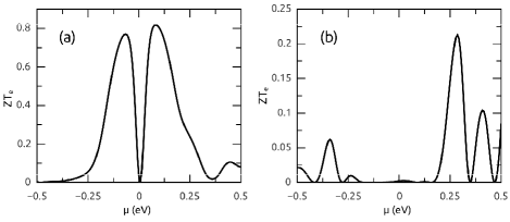
Based on the energy bands, we calculate the thermoelectric coefficients of the two-dimensional silicene and germanene structures at room temperature, . To perform the calculation of the figure of merit we have evaluated the transport coefficients given in Eqs. (2)-(4) in the constant relaxation time approximation. We have used the BoltzTraP codeMadsen and Singh (2006) to perform the integration in the first Brillouin-zone obtained from the VASP calculations. As we discussed in the introduction, we provide an upper bound to , in the form of the electronic figure of merit . We notice that the electronic figure of merit is independent of the relaxation time, thus justifying the use of the BoltzTraP. Figures 2(a) and (b) show the dimensionless electronic figure of merit, as a function of the chemical potential for the distorted silicene and germanene, respectively. It can be seen that the figure of merit for silicene exhibits two peaks in the left- and right-hand sides of , which separately correspond to the hole and electron transport. The maximum of the peak is about , while for the unsupported germanene, it can be seen from Fig. 2(b) that the peak of is very small at , although some peaks appear at eV. The reason is that the unsupported germanene has a metallic character which leads to a very small Seebeck coefficient.
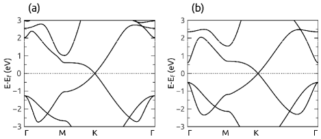
In Fig. 3 we show the electronic properties of free standing silicene and germanene. After the full relaxation, it is found that the buckling distance for silicene is about 0.43 Å, and for germanene 0.65 Å. For both the free standing silicene and germanene, from Figs. 3(a) and (b) it can be seen that there is no gap at the Fermi energy. Indeed, at the high symmetry point K, a linear energy dispersion is shown in the band structures, indicating the existence of the massless Dirac fermions in these low dimensional Si structuresCahangirov et al. (2009) similar to the graphene.Castro Neto et al. (2009)
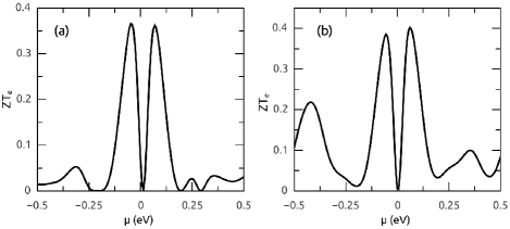
Through the energy band structure calculations, in Fig. 4 we investigate the dimensionless electronic figure of merit for both free standing silicene and germanene. It is found that the figure of merit for silicene and germanene shows two peaks near . The maximum value of is 0.36 (see Fig. 4(a)), while the maximum of the peak for germanene is 0.41 (see Fig. 4(b)).
We have shown that silicene and germanene, crystal structures similar to graphene where carbon is replaced by either silicon or germanium, might possibly have a figure of merit of the order of 1. Our calculations provide an upper limit to the theoretical figure of merit since in these calculations we are not including the phonon thermal conductance and suggest that silicene might have a better thermoelectric properties in this 2D system since it does present a gap in the electronic energy spectrum which corresponds to a large Seebeck coefficient.
IV Quasi-one-dimensional nano-structures
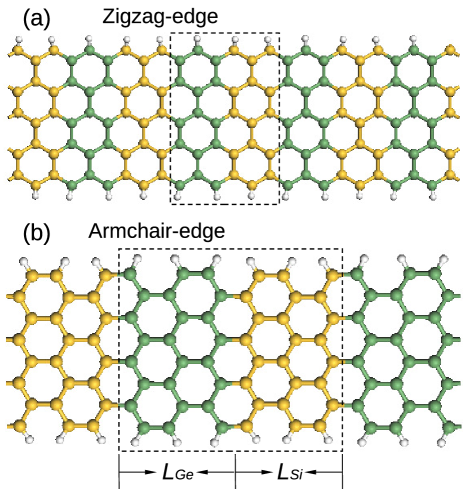
We now consider quasi-one-dimensional systems, nano-ribbons, made of stripes of germanene or silicene of finite width. We assume that it is possible to “cut” those stripes from the respective crystal by removing the excess material. It has been reported that SiNRs can have a quite large figure of merit, up to 5 at 600 K.Pan et al. (2012) Motivated by these results, and by the expectation than germanene nano-ribbons might perform better since their Debye temperature is lower, we have investigated the thermoelectric efficiency of GeNRs and, in the next session, nano-ribbons obtained by alternating Si and Ge nano-structures or by randomising the Si and Ge arrangements. As standard with nano-ribbons, there are two ways to terminate the edges of the ribbons (see Fig. 5), forming either zigzag or armchair edges. We identify the quantities associated with the zigzag with a Z and those of the armchair with a A. As to these one-dimensional systems, the electrical conductance , Seebeck coefficient , and thermal conductance could be contracted into a scalar instead of a tensor, and the and are fixed in the direction (see details in Ref. Yang et al., 2012). Therefore in this case we can calculate the electron and phonon transmissions by counting the number of transport modes from the energy band. This gives the same results by comparing them with the constant relaxation time approximation in Eq. (7) except by an amplitude factor difference.
IV.1 Germanene nano-ribbons
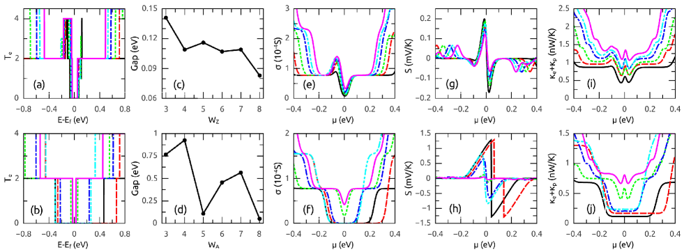
Figures 5(a) and (b) show the optimized structures of zigzag- and armchair-edged GeNRs (Z-GeNRs and A-GeNRs), respectively. To see more clearly the buckling, we report here a side view of these structures. Hydrogen atoms are used to passivate the unsaturated bonds of the Ge atoms at the edges. and identify the ribbon width. It can be seen from the top view that GeNRs form hexagonal rings as the union of two sub-lattices, but, at odds with what happens for graphene nano-ribbons, atoms in these two sub-lattices do not belong to the same plane: in the vertical direction there is some buckling, which is almost uniform for the atoms at the edge or in the center. Our calculations give for the Z-GeNRs a buckling distance of 0.62 Å, while for A-GeNRs give 0.66 Å. For these nano-ribbons, our total energy calculations show that the anti-ferromagnetic (AFM) state of Z-GeNRs is more stable than the ferromagnetic (FM) and non-magnetic (NM) states counterparts. This is in agreement with other calculations performed for SiNRsPan et al. (2012) and theoretical predictions originally derived for graphene, which we expect to be valid for these systems.Jung et al. (2009) However, the energy difference between the different magnetic phases is small. This might be important for device stability especially at temperatures higher than 300 K. The bands of AFM and FM states are shown in Figs. 5 (c) and (d), respectively, where the dotted line corresponds to the Fermi energy. We can see that AFM state exhibits a finite small gap: The bands for spin up and down are degenerate and the gap is about 0.1 eV. While for the FM state, it is found that spin up and down are non-degenerate, producing metallic properties, and similar properties are valid for the NM state (not shown). In the case of A-GeNR, our calculations indicate that the NM state is stable, indicating semiconducting properties as shown in Fig. 5 (e). Because the metallic system produces bad thermoelectric properties (generally the is smaller than 0.1), in the rest part of this work, we will focus the attentions on the AFM state in the zigzag-edged nano-ribbons and NM state in the armchair-edged nano-ribbons. To confirm the structural stability of GeNRs, we have calculated the phonon dispersion relations. In Figs. 5 (f) and (g) we report the phonon dispersion relation for the nano-ribbons with width 6 for both Z-GeNR and A-GeNR, i.e., , respectively. It can be seen that in the limit of , there are four acoustic phonon modes in the spectrum stemming from the lattice symmetry. In particular, no negative phonon mode is observed, which confirms that both the Z-GeNRs and A-GeNRs passivated by hydrogen are structurally stable.
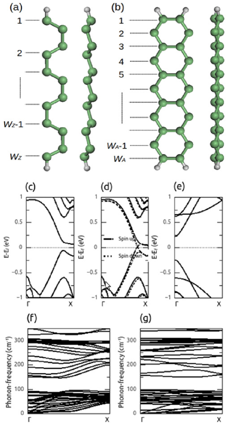
To calculate the figure of merit , we begin with the electron transport properties. Figures 6(a) and (b) show the transmission coefficient as a function of the electron energy for both Z-GeNRs and A-GeNRs, respectively. It can be seen that exhibits a clear quantum stepwise structure, due to opening and closing of elastic transmission channels: notice that the jumps are quantized and equal to 2 due to the electron spin. More interesting, a monotonously decreasing band gap is observed in the Z-GeNRs with the increasing of the ribbon width (see Fig. 6(c)). This must be compared with the oscillatory behaviour we observe for the A-GeNRs (see Fig. 6 (d)). For the A-GeNRs, for the ribbon widths and (where is positive integer), the gap is larger than that of the ribbon width . By making use of the transmission probability, using Eqs. (2)-(3), we can calculate the electrical conductance , Seebeck coefficient and electron contributed thermal conductance . In Figs. 6 (e) and (f), the electrical conductance as a function of chemical potential is plotted for both Z-GeNRs and A-GeNRs, respectively. It can be seen that the electrical conductance for zigzag nano-ribbons gradually increases with the ribbon width, and there is a peak corresponding the transmission step at eV. Around the Fermi energy, the conductance vanishes due to the finite gap. For the A-GeNRs, we find that the electrical conductance for the ribbon with width or vanishes, while for the ribbon with width , a non-zero dip is found. Interestingly, the conductance for all the curves of A-GeNRs exhibits quantized plateau-like characteristics.
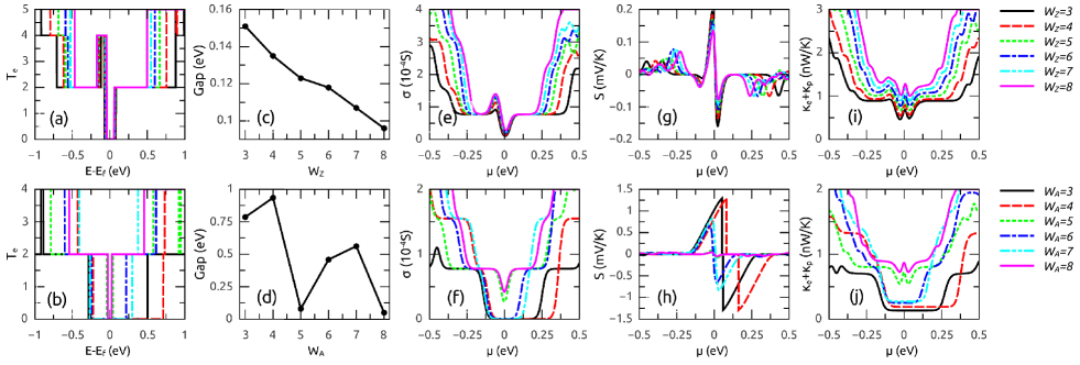
In Fig. 6 (g) and (h) we report the Seebeck coefficient as a function of the chemical potential . It can be seen from Fig. 6(g) that presents two peaks around the position of the chemical potential needed to overcome the gap. Moreover the two peaks show different sign with positive and negative values. This behavior indicates the different carrier transport: the positive sign in the region of corresponds to hole transport, while the negative at corresponds to electron transport. In addition the absolute value of the peak of the Seebeck coefficient decreases with increasing . In the case of A-GeNRs, it is found (see Fig. 6 (h)) that for the nano-ribbons with width and , the two Seebeck coefficient peaks with opposite sign can also be found centred around zero value of the chemical potential. We note that for the nano-ribbons with width , the Seebeck coefficient is very small due to the small electronic gap. In Figs. 6 (i) and (j) the total thermal conductance for Z-GeNRs and A-GeNRs is depicted, respectively. It can be seen that the thermal conductance for Z-GeNRs increases with increasing the width of the nano-ribbon. By checking the variation of the electrical and thermal conductances, and , it is found that corresponding to the dip position of the electrical conductance, the electric thermal conductance (and therefore the total thermal conductance) shows a peak which becomes sharper with increasing . Moreover, a similar effect can also be found in the A-GeNRs with width as shown in Fig. 6(j).
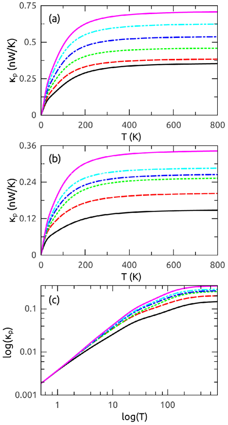
To study the lattice thermal transport properties, the supercell approach is utilised to calculate the phonon force constant and then the dispersion relation is obtained by diagonalizing the corresponding dynamical matrix.Alfè (2009) In Figs. 7 (a) and (b), the phonon thermal conductance as a function of temperature for both Z-GeNRs and A-GeNRs is plotted, respectively. It can be seen that the phonon thermal conductance increases with increasing the temperature, and finally reaches a constant value corresponding to the classical limit when K. Moreover the thermal conductance for wide nano-ribbons exhibits a higher value than that of the narrow nano-ribbons. This can simply be explained by “counting” the number of phonon channels, because the wide nano-ribbons should have more phonon channels contributing to the thermal transport. To show the behaviour at low temperatures of the phonon thermal conductance, in Fig. 7 (c), we plot the logarithm of versus the logarithm of . It can be seen that shows a linear dependence on the temperature at low , K. At low temperature, for the one-dimensional systems, the lattice thermal conductance is dominated by the low-frequency acoustic phonons, and the Eq. (4) can be recast as
| (10) |
where and we have approximated the transmission probability because of the sum rule. According to this approximation, it can be seen that the phonon thermal conductance exhibits a linear dependence on in quasi-one-dimensional systems.Yamamoto and Watanabe (2006)
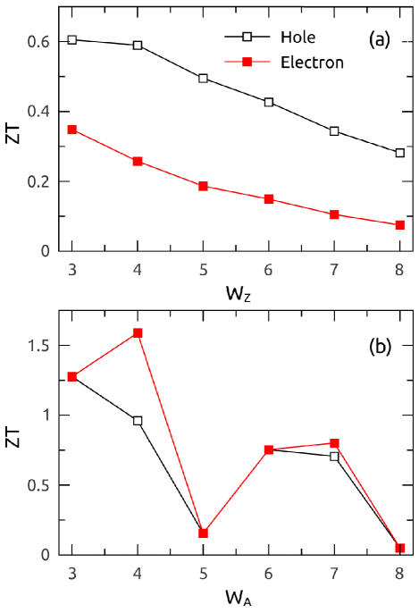
By combining the results of the electron and phonon calculations, we can finally investigate the thermoelectric efficiency of the GeNRs. Figures 8(a) and (b) report the thermoelectric figure of merit as a function of the ribbon width for both Z-GeNRs and A-GeNRs, respectively. Here is the maximum value of the figure of merit with respect to the chemical potential near the Fermi energy. It can be seen from Fig. 8 (a) that at narrow Z-GeNRs, for electron and hole is about 0.35 and 0.61, and then it decreases with increasing the ribbon width. This effect can be explained by the lessening of the Seebeck coefficient and growing of the thermal conductance outweighing the increasing electrical conductance. Moreover, we observe from Fig. 8(b) for the A-GeNRs, that the for both electron and hole transport coefficients show an oscillatory behavior. In the case of the nano-ribbons with width and , is larger than 1 for narrow nano-ribbons. In particular for the ribbon width , the reaches up to 1.63, indicating a high thermoelectric conversion efficiency in these nano-structures.
Our results are consistent with what has been found for SiNRs.Pan et al. (2012) However, we would like to point out that from our calculations the phonon thermal conductance of the small GeNR is never negligible with respect to the electron thermal conductance, as instead has been argued for the SiNRs in Ref. Pan et al., 2012. We believe this is an artefact of the classical methods used in Ref. Pan et al., 2012. Indeed, we expect that the classical methods would not recover the linear behavior with temperature of the phonon thermal conductance at small temperatures of these quasi-one-dimensional systems in the ballistic thermal transport regime as we do in our quantum simulations. Moreover, the classical calculations should be valid for temperatures larger than the Debye temperature, that for these systems can be estimated to be about 600 K for silicene nano-ribbons. At the same time, the quantum technique does not include any inelastic effect and it is strongly limited in size, i.e., we cannot consider a large supercell as instead is possible with classical methods.Pan et al. (2012)
IV.2 Silicene nano-ribbons
For completeness, and to have a direct comparison with the results available in the literature,Pan et al. (2012) we have calculated, the figure of merit of SiNRs, similar to the GeNRs we have investigated in the previous section. Here we report only the phonon thermal conductance and the figure of merit. The electron transport coefficients, , , and have shapes similar to those in Fig. 6 and we do not show them again. We plot in Figs. 9 (a) and (b), the phonon thermal conductance for both zigzag- and armchair-edged SiNRs (Z-SiNRs and A-SiNRs) as a function of temperature , respectively. It is seen that the phonon thermal conductance increases with the temperature, and finally reaches a steady value. For the zigzag nano-ribbons, the thermal conductance increases gradually with the ribbon width due to the increase in available phonon transport channels. As to the armchair nano-ribbons, the thermal conductance is also increased except for the ribbon width whose values are tightly close (see Fig. 9 (b)).
In Fig. 10 the figure of merit for SiNRs as a function of ribbon width is shown. It can be seen that the figure of merit for Z-SiNRs decreases with the increase of the ribbon width. Moreover the for the hole transport is larger than that contributed from the electron transport. The reason is due to the increased phonon thermal conductance and decreased electronic band gap. For the armchair nano-ribbons, it is found from Fig. 10 (b) that the figure of merit at narrow ribbon is quite large, about 1.04. With the increase of the ribbon width, the decreases overall and exhibits an oscillatory behavior.
V Silicon-germanium hetero-structures
We have shown that the Si and Ge nano-ribbons can have a substantial figure of merit, which is slightly above 1. On the other hand, we would like to explore the possibility of improving on this result by nano-structuring these nano-ribbons. Since Si and Ge nano-ribbons do share similar electronic properties, our first attempt is to investigate a nano-ribbon created by alternating stripes of Si and Ge in the direction of the growth of the nano-ribbon. Hopefully, their different masses would create a trap for the phonon modes thus reducing the thermal conductance of the device and improving the overall figure of merit . We will show in the following sub-section that this idea is working partially and we do have a modest increasing of . This is a limitation of our quantum method of calculating the thermal conductance, since we are limited in the size of the supercell we can consider for our calculations. Indeed, the low energy phonons responsible primarily for the thermal transport have a wavelength that spans many supercells thus making the chemical modulation ineffective as a phonon trap. To improve on this result, we have therefore investigated the case where we randomly substituted some Si atoms with Ge in the nano-ribbon crystal. After fully relaxing the structure, we have however observed that also this nano-ribbon with randomly distributed Si and Ge atoms does not work too much as a phonon trap, for essentially the same reason of the perfect modulation: the Si and Ge randomly distributed supercell is not large enough to confine the low energy phonon modes. We checked this observation by using a tight-binding approximation to calculate the phonon spectrum. This allows us to reach larger a supercell and thus show that the phonon thermal conductance decreases due to the phonon confinement in these random structures.
V.1 Thermoelectric properties of the silicene-germanene nano-ribbons
In this section, we investigate the thermoelectric properties of orderly-distributed hetero-structured silicene-germanene nano-ribbons (SiGeNRs). After forming the structure, we have relaxed the atomic positions, without taking into account any substrate. Figure 11 shows the optimized geometrical structures of zigzag- and armchair-edged SiGeNRs (Z-SiGeNRs and A-SiGeNRs) passivated by hydrogen atoms, where the line encloses a supercell along the ribbon axis. and are the length of silicene and germanene stripes in the supercell, respectively.
We begin with the case . In Figs. 12 (a) and (b) we report the transmission coefficient as a function of electron energy for different width of the Z-SiGeNRs and A-SiGeNRs, respectively. It can be seen that the transmission probability exhibits characteristic quantized steps and a band gap is shown around the Fermi energy. Increasing the ribbon width, the band gap for Z-SiGeNRs shows an oscillatory behaviour of decreasing amplitude from to 7 (see Fig. 12 (c)), while the gap for A-SiGeNRs shows a strongly oscillatory behaviour as shown in Fig. 12 (d). When the ribbon width satisfies either , a larger gap appears than that of the nano-ribbons with width . This width dependence of the band gap is similar to that of the A-GeNRs and A-SiNRs as we have discussed in section IV. Starting from this transmission function we can now easily evaluate the Eq. 2-4 to obtain the transport coefficients. In Figs. 12 (e) and (f) we plot the electrical conductance as a function of the chemical potential in the linear response. It is found that the electric conductance for Z-SiGeNRs exhibits a peak and a dip around . As for the A-SiGeNRs, we show that the electrical conductance is zero for the nano-ribbon with width , due to the presence of the larger band gap, while the conductance for the ribbon with width has a dip at where the conductance assumes a finite value. In Figs. 12 (g) and (h), the Seebeck coefficient versus chemical potential is depicted. It is found that in the Seebeck coefficient, around two peaks appear for both Z-SiGeNRs and A-SiGeNRs with width , . The absolute value of the peak for A-SiGeNRs is 1.4 mV/K, which is quite larger than the value of the Z-SiGeNRs, indicating a quite high thermoelectric effect in this armchair-edged nano-ribbons. On the other hand, for the armchair nano-ribbons with width , the Seebeck coefficient is very small due to the very small gap present in these systems. In Figs. 12 (i) and (j) the total thermal conductance including electron and phonon contributions is plotted. It can be seen that for Z-SiGeNRs exhibits a peak, while for the A-SiGeNRs with widths and , it has a plateau in the energy region around , mostly due to the phonon thermal transport. As for the nano-ribbon with width , the thermal conductance reaches a local maximum on account of a local maximum of the electron heat contribution at .
Figures 13 (a) and (b) show the phonon thermal conductance for both Z-SiGeNRs and A-SiGeNRs as a function of temperature for different nano-ribbon widths, respectively. It can be seen that the phonon thermal conductance increases gradually with increasing the temperature and finally reaches a plateau at K. This value is compatible with the value reported in the classical thermal transport theory. By comparing Fig. 13 with Figs. 7 and 9, we find that the thermal conductance of SiGeNRs is between the value of GeNRs and SiNRs, i.e., the thermal conductance of SiGeNRs is larger than that of GeNRs, while smaller than that of SiNRs. Similar to the case of GeNRs or SiNRs, at low temperature region, the linear dependence of the thermal conductance on the temperature is still observed, in agreement with Eq. (10).
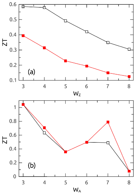
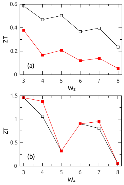
In Figs. 14 (a) and (b), we report the figure of merit of both Z-SiGeNRs and A-SiGeNRs as a function of ribbon widths and , respectively. It is found that maximum value of the figure of merit for Z-SiGeNRs appears in the narrowest nano-ribbon, which is about 0.59 corresponding to the hole transport. While for the electron transport, the corresponding is about 0.38. As to the armchair-edged nano-ribbon with width , the is found to be 1.46 for both the hole and electron transport (see Fig. 14 (b)). With the increase of the ribbon width, the figure of merit shows an oscillatory behavior reminiscent of the different properties of the nano-ribbons with different widths. The amplitude of the “oscillation” however decreases quite rapidly with increasing the ribbon width. This is mostly due to the rapid increasing of the phonon thermal conductance with . In particular, the is very small in the case of nano-ribbon with width due to the small Seebeck coefficient as shown in Fig. 12 (h).
V.2 Component modulation of the thermoelectrics in the silicene-germanene nanoribbons
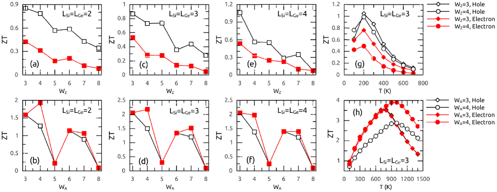
In Fig. 15, we investigate the thermoelectric properties of SiGeNRs by modulating the component lengths of silicene and germanene stripes in the supercell. In the following, the total length of the supercell is given by . Figures 15 (a) and (b), (c) and (d), (e) and (f) show the figure of merit at room temperature for Z-SiGeNRs and A-SiGeNRs as a function of ribbon width for , and , respectively. It is found that the maximum for hole and electron transport in the case of the Z-SiGeNRs is 0.85 and 0.42 for , 0.87 and 0.53 for , and 1.06 and 0.54 for , respectively. For armchair nano-ribbons, the maximum of for is about 1.93, while the maximum for or is about 2.18 and 2.06, respectively. With the increase of the ribbon width, the overall figure of merit decreases for both Z-SiGeNRs and A-SiGeNRs with width and . As to the nano-ribbon with width , the figure of merit is quite small compared to the ribbons with width or . We found that the Seebeck coefficient for nano-ribbon with width is very small due to the small band gap, in agreement with our analysis of the system with . Figures 15 (g) and (h) show the figure of merit as a function of temperature for Z-SiGeNRs with width and A-SiGeNRs with width , respectively. It can be seen that the figure of merit increases and then decreases with increasing the temperature. The maximum for Z-SiGeNRs is about 1.05 at K, and the maximum for A-SiGeNRs is about 3.91 at K.
We wish to point out that the of these systems is larger than that for the pure A-GeNRs or A-SiNRs. This means that nano-structuring can improve the overall energy conversion efficiency. On the other hand, the modest increase in for these nano-ribbons shows how this nano-structuring is not effective in blocking the phonon modes. We should reach larger and , in order to achieve an efficient trapping of the low energy phonon modes, as we will discuss briefly at the end of next sub section.
V.3 Disorder effect on the thermoelectrics of silicene-germanene nano-ribbons
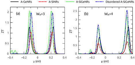
In the above discussions, the Si and Ge atoms in the nano-ribbons are orderly distributed along the growth direction. Here we consider the case in which Si and Ge atoms randomly occupy with equal probability the sites of the lattice in Fig. 11. The length of the supercell is and the number of Si and Ge atoms in the supercell are taken the same. Since the armchair nano-ribbons show the most promising values of the figure of merit, in Figs. 16 (a) and (b) we report the figure of merit as a function of the chemical potential for disordered A-SiGeNRs with the ribbon width and , respectively. As a comparison, we have also plotted the figure of merit for A-GeNRs, A-SiGRs and A-SiGeNRs. It can be seen that the maximum figure of merit for disordered A-SiGeNRs and ordered A-SiGeNRs is nearly twice of the value of clean A-GeNRs and A-SiGRs. The maximum for disordered and ordered A-SiGeNRs with width is about 2 for both electron and hole transport corresponding to the positive and negative chemical potential, while the maximum for the ribbon width is 2.18 and 2.56 for electron and 1.5 and 1.8 for hole transport, respectively. The principal reason of the enhanced thermoelectric efficiency comes from the reduced phonon thermal conductance, since the electronic properties are slightly affected by the randomness of the atomic positions. Again, due to the small size of the supercell we can consider with ab-initio techniques, phonon confinement is not efficient, and therefore the thermal conductance of disordered and ordered A-SiGeNRs is only slightly reduced with respect to the clean Si and Ge system as shown in comparing Figs. 15 and 16. For the same reason, the thermal conductance of the random structure is similar to the one of the silicene-germanene hetero-structures as expected.
To present a proof that a large supercell can effectively further reduce the phonon thermal conductance in the SiGe hetero-structures, we use a semi-classical tight-binding method to investigate the lattice thermal transport properties. To obtain the atomic force constant of the system, the Keating potential is used,Rücker and Methfessel (1995); Wang et al. (2008); Davydov (2012) which is given by
| (11) | |||||
where and are the equilibrium position vectors connecting atom with and , and are the corresponding position vectors after deformation, respectively. The bond stretching and bending force parameters and for silicene in Eq. (11) are 7.2186 N/m3 and 1.5225 N/m3. These constants can be obtained from the force constants of graphene.Davydov (2010, 2012) In our case we have used
| (12) |
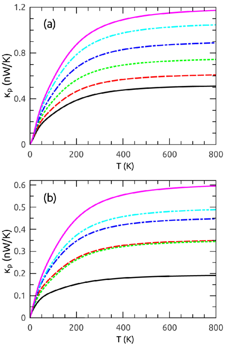
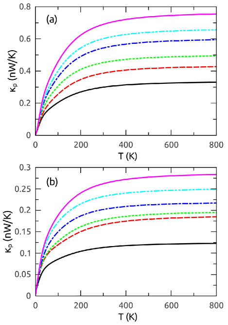
where N/m2 and N/m2 for siliceneDavydov (2010, 2012) and is the equilibrium distance of the Si atoms in the silicene structure, that we have calculated as Å. We have then fine tuned the values of and to improve the agreement between the phonon spectrum (not shown) calculated via ab-initio and the one calculated within the tight-binding approximation. For the parameters of germanene, we roughly estimate N/m3 and N/m3 through comparing the force constant ratio of this 2D system with the bulk silicon and germanium crystals.Rücker and Methfessel (1995) We have again fine tuned these values to improve the agreement between the ab-initio and tight-binding phonon spectra. For the force parameters between Si and Ge atoms in the hybrid structures, we take their average value. As to the Si-H and Ge-H interactions, we take ten percent of the corresponding Si-Si and Ge-Ge interactions, accordingly. Based on this Keating model and combined with the non-equilibrium Green’s function technique, we can calculate the phonon transmission probability and thus the thermal transport properties (see details in Ref. Yang et al., 2012). Figures 17 (a) and (b) show the phonon thermal conductance calculated from tight-binding (gray lines) for A-GeNRs, A-SiNRs, A-SiGeNRs and disordered A-SiGeNRs, where the ribbon width . To check how reliable is the tight-binding calculations, we report together the thermal conductance calculated from ab-initio (color lines in Fig. 17(a)). It can be seen that the thermal conductance obtained from tight-binding and ab-initio are quite close, especially in the low temperature region. In addition, it is found that the phonon thermal conductance in the case of A-SiGeNRs and disordered A-SiGeNRs is drastically decreased compared to the pure A-SiNRs and A-GeNRs. With further increasing the length of the supercell, the phonon thermal conductance is decreasing as shown in Fig. 17(b).
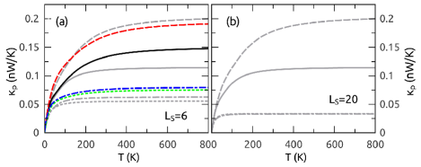
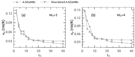
In Fig. 18, the phonon thermal conductance at T=300 K for both A-SiGeNRs and disordered A-SiGeNRs as a function of supercell length is investigated, where is defined as the sum of the length of silicene and germanene stripes. It can be seen that the phonon thermal conductance decreases with increasing the length of the supercell, and the for both A-SiGeNRs and disordered A-SiGeNRs are close to each other. This indicates that the larger supercell in the silicene-germanene hetero-structures can effectively constrain the phonon transport and that the disordered heterostructure becomes more efficient in confining phonons only at large unit cell lengths. Through checking the transmission probability (not shown), it is found that the weight of the transmission probability is gradually moved to the low frequency region thus decreasing the total energy flow.
VI Conclusions
In summary, we have performed first-principle calculations of the thermoelectric coefficients of both two-dimensional silicene and germanene as well as for Si and Ge nano-ribbons. We have also considered hetero-structures of Si and Ge stripes to form a nano-ribbon, in the attempt to quench the phonon dynamics and thus increasing the figure of merit. These systems can be good thermoelectric materials if they can be reliably produced. Also, being based on Si and Ge, we expect these devices to be easily interfaced with the modern electronic systems, a distinct advantage with respect to other materials which have shown poor integrability with the actual technology.
The figure of merit for thermoelectric energy conversion of Si and Ge low dimensional systems is quite high, in the range 1 to 2 at room temperature, considering that we have investigated pristine systems where phonons are not confined. For the silicene and germanene systems we have considered both distorted silicene/germanene grown on a silver surface and free-standing silicene/germanene. In these cases we have found the highest figure of merit is about 0.81 for the distorted silicene. It is important to point out that Si/Ge nano-sheets grown on a Ag surface show different electrical properties according to the lattice matching: we have considered a 33 Si lattice on a 44 Ag substrate since this induces no stress at the supercell edges and when the Ag substrate is removed, the distorted silicene has a finite band gap. It is indeed clear from our calculations that in order to increase the figure of merit, we need to have a small gap semiconductor since this maximizes the Seebeck coefficient.
Our attempts to quench the phonon dynamics have been hindered by the small scale of the supercell we can calculate with our ab-initio techniques. We could in principle go beyond these limitations by using other classical tools like, e.g., molecular dynamics. However, especially for the nano-ribbons, in our tests (not reported here) these tools have proven unable to recover the quantum of thermal conductance at small temperatures. We have therefore chosen to test the phonon confinement with semi-empirical techniques, e.g., a tight-binding calculation of the phonon thermal transport for large supercell. We report that the thermal conductance is effectively reduced by about 50% in going from a supercell made of 6 units to a supercell made of 20 units.
Acknowledgements.
We thank Y. Pouillon and A. Iacomino for providing some computational help. We acknowledge financial support from CONSOLIDER INGENIO 2010: NANOTherm (CSD2010-00044), Diputacion Foral de Gipuzkoa (Q4818001B), the European Research Council Advanced Grant DYNamo (ERC-2010-AdG-267374), Spanish Grants (FIS2010-21282-C02-01), Grupos Consolidados UPV/EHU del Gobierno Vasco (IT578-13), Ikerbasque, and MAT2012-33483. Computational time was granted by i2basque and BSC “Red Española de Supercomputacion”.References
- Pollock (1985) D. Pollock, Thermoelectricity; theory, thermometry, tool (ASTM, Philadelphia, 1985).
- Nolas et al. (2001) G. S. Nolas, J. Sharp, and H. J. Goldsmid, Thermoelectrics: basic principles and new materials developments, Springer Series in Material Science, Vol. 45 (Springer Verlag, Berlin Heidelberg, 2001).
- Goldsmid (2010) H. J. Goldsmid, Springer Ser. Mater. Sci., 1st ed. (Springer-Verlag, Berlin, 2010) p. 250.
- DiSalvo (1999) F. J. DiSalvo, Science 285, 703 (1999).
- Vining (2009) C. Vining, Nature Mater. 8, 83 (2009).
- Venkatasubramanian et al. (2001) R. Venkatasubramanian, E. Siivola, T. Colpitts, and B. O’Quinn, Nature 413, 597 (2001).
- Ashcroft and Mermin (1976) N. W. Ashcroft and N. D. Mermin, Solid State Physics (Saunders College Publishing, 1976).
- Hicks and Dresselhaus (1993) L. D. Hicks and M. S. Dresselhaus, Phys. Rev. B 47, 12727 (1993).
- Minnich et al. (2009) A. J. Minnich, M. S. Dresselhaus, Z. F. Ren, and G. Chen, Energy Environ. Sci. 2, 466 (2009).
- Pichanusakorn and Bandaru (2010) P. Pichanusakorn and P. Bandaru, Mater. Sci. Eng. R Reports 67, 19 (2010).
- Novoselov et al. (2004) K. S. Novoselov, A. K. Geim, S. V. Morozov, D. Jiang, Y. Zhang, S. V. Dubonos, I. V. Grigorieva, and A. A. Firsov, Science 306, 666 (2004).
- Balandin et al. (2008) A. Balandin, S. Ghosh, W. Bao, I. Calizo, D. Teweldebrhan, F. Miao, and C. N. Lau, Nano Lett. 8, 902 (2008).
- Seol et al. (2010) J. H. Seol, I. Jo, A. L. Moore, L. Lindsay, Z. H. Aitken, M. T. Pettes, X. Li, Z. Yao, R. Huang, D. Broido, N. Mingo, R. S. Ruoff, and L. Shi, Science 328, 213 (2010).
- Prasher (2010) R. Prasher, Science 328, 185 (2010).
- Yang et al. (2012) K. Yang, Y. Chen, R. D’Agosta, Y. Xie, J. Zhong, and A. Rubio, Phys. Rev. B 86, 045425 (2012).
- Hochbaum et al. (2008) A. I. Hochbaum, R. Chen, R. D. Delgado, W. Liang, E. C. Garnett, M. Najarian, A. Majumdar, and P. Yang, Nature 451, 163 (2008).
- Castro Neto et al. (2009) A. H. Castro Neto, N. M. R. Peres, K. S. Novoselov, and A. K. Geim, Rev. Mod. Phys. 81, 109 (2009).
- Peres (2010) N. M. R. Peres, Rev. Mod. Phys. 82, 2673 (2010).
- Ayala et al. (2010) P. Ayala, A. Rubio, and T. Pichler, Rev. Mod. Phys. 82, 1843 (2010).
- Das Sarma et al. (2011) S. Das Sarma, S. Adam, E. H. Hwang, and E. Rossi, Rev. Mod. Phys. 83, 407 (2011).
- Kotov et al. (2012) V. N. Kotov, B. Uchoa, V. M. Pereira, F. Guinea, and A. H. Castro Neto, Rev. Mod. Phys. 84, 1067 (2012).
- Cahangirov et al. (2009) S. Cahangirov, M. Topsakal, E. Aktürk, H. Sahin, and S. Ciraci, Phys. Rev. Lett. 102, 236804 (2009).
- Chen et al. (2012) L. Chen, C.-C. Liu, B. Feng, X. He, P. Cheng, Z. Ding, S. Meng, Y. Yao, and K. Wu, Phys. Rev. Lett. 109, 056804 (2012).
- Bechstedt et al. (2012) F. Bechstedt, L. Matthes, P. Gori, and O. Pulci, Appl. Phys. Lett. 100, 261906 (2012).
- De Padova et al. (2010) P. De Padova, C. Quaresima, C. Ottaviani, P. M. Sheverdyaeva, P. Moras, C. Carbone, D. Topwal, B. Olivieri, A. Kara, H. Oughaddou, B. Aufray, and G. Le Lay, Appl. Phys. Lett. 96, 261905 (2010).
- Lalmi et al. (2010) B. Lalmi, H. Oughaddou, H. Enriquez, A. Kara, S. Vizzini, B. Ealet, and B. Aufray, Appl. Phys. Lett. 97, 223109 (2010).
- De Padova et al. (2012) P. De Padova, O. Kubo, B. Olivieri, C. Quaresima, T. Nakayama, M. Aono, and G. Le Lay, Nano Lett. 12, 5500 (2012).
- Kara et al. (2012) A. Kara, H. Enriquez, A. P. Seitsonen, L. Lew Yan Voon, S. Vizzini, B. Aufray, and H. Oughaddou, Surf. Sci. Rep. 67, 1 (2012).
- Feng et al. (2012) B. Feng, Z. Ding, S. Meng, Y. Yao, X. He, P. Cheng, L. Chen, and K. Wu, Nano Lett. 12, 3507 (2012).
- Enriquez et al. (2012) H. Enriquez, S. Vizzini, A. Kara, B. Lalmi, and H. Oughaddou, J. Phys. Condens. Matter 24, 314211 (2012).
- Jamgotchian et al. (2012) H. Jamgotchian, Y. Colignon, N. Hamzaoui, B. Ealet, J. Y. Hoarau, B. Aufray, and J. P. Bibérian, J. Phys. Condens. Matter 24, 172001 (2012).
- Vogt et al. (2012) P. Vogt, P. De Padova, C. Quaresima, J. Avila, E. Frantzeskakis, M. C. Asensio, A. Resta, B. Ealet, and G. Le Lay, Phys. Rev. Lett. 108, 155501 (2012).
- Lin et al. (2013) C.-L. Lin, R. Arafune, K. Kawahara, M. Kanno, N. Tsukahara, E. Minamitani, Y. Kim, M. Kawai, and N. Takagi, Phys. Rev. Lett. 110, 076801 (2013).
- Chen et al. (2013) L. Chen, H. Li, B. Feng, Z. Ding, J. Qiu, P. Cheng, K. Wu, and S. Meng, Phys. Rev. Lett. 110, 085504 (2013).
- Meng et al. (2013) L. Meng, Y. Wang, L. Zhang, S. Du, R. Wu, L. Li, Y. Zhang, G. Li, H. Zhou, W. A. Hofer, and H.-J. Gao, Nano Lett. 13, 685 (2013).
- Cahangirov et al. (2013) S. Cahangirov, M. Audiffred, P. Tang, A. Iacomino, W. Duan, G. Merino, and A. Rubio, Phys. Rev. B 88, 035432 (2013).
- Li et al. (1994) G. H. Li, A. R. Goni, C. Abraham, K. Syassen, P. V. Santos, A. Cantarero, O. Brandt, and K. Ploog, Phys. Rev. B 50, 1575 (1994).
- Pan et al. (2012) L. Pan, H. J. Liu, X. J. Tan, H. Y. Lv, J. Shi, X. F. Tang, and G. Zheng, Phys. Chem. Chem. Phys. 14, 13588 (2012).
- D’Agosta (2013) R. D’Agosta, Phys. Chem. Chem. Phys. 15, 1758 (2013).
- Landauer (1957) R. Landauer, IBM J. Res. Dev. 1, 223 (1957).
- Baranger and Stone (1989) H. U. Baranger and A. D. Stone, Phys. Rev. B 40, 8169 (1989).
- Yamamoto and Watanabe (2006) T. Yamamoto and K. Watanabe, Phys. Rev. Lett. 96, 255503 (2006).
- Kresse and Furthmüller (1996) G. Kresse and J. Furthmüller, Phys. Rev. B 54, 11169 (1996).
- Ceperley and Alder (1980) D. M. Ceperley and B. J. Alder, Phys. Rev. Lett. 45, 566 (1980).
- Perdew and Zunger (1981) J. P. Perdew and A. Zunger, Phys. Rev. B 23, 5048 (1981).
- Alfè (2009) D. Alfè, Comput. Phys. Commun. 180, 2622 (2009).
- Madsen and Singh (2006) G. K. Madsen and D. J. Singh, Comput. Phys. Commun. 175, 67 (2006).
- Jung et al. (2009) J. Jung, T. Pereg-Barnea, and A. H. MacDonald, Phys. Rev. Lett. 102, 227205 (2009).
- Rücker and Methfessel (1995) H. Rücker and M. Methfessel, Phys. Rev. B 52, 11059 (1995).
- Wang et al. (2008) J. Wang, Q.-A. Huang, and H. Yu, J. Phys. D: Appl. Phys. 41, 165406 (2008).
- Davydov (2012) S. Y. Davydov, Phys. Solid State 54, 652 (2012).
- Davydov (2010) S. Y. Davydov, Phys. Solid State 52, 184 (2010).