Photo-induced doping and strain in exfoliated graphene
Abstract
The modification of single layer graphene due to intense, picoseconds near-infrared laser pulses is investigated. We monitor the stable changes introduced to graphene upon photoexcitation using Raman spectroscopy. We find that photoexcitation leads to both a local increase in hole doping and a reduction in compressive strain. Possible explanations for these effects, due to photo-induced oxygenation and photo-induced buckling of the graphene, are discussed.
The unique electrical and optical properties of graphene have made it a very promising material for future electro-optical applications. One of graphene most appealing aspects, due to its interfacial nature, is its tunability. For example, it is well known that the band structure and conduction properties of graphene can be modified and functionalized by molecular adsorbatesWehling et al. (2008); Wehling, Lichtenstein, and Katsnelson (2008); Wang et al. (2010); Chen et al. (2007); Robinson et al. (2010), by irradiation under electron beamsTeweldebrhan and Balandin (2009); Fischbein and Drndic (2008); Withers et al. (2011); Sessi et al. (2009), by applied electric and magnetic fieldsCastro et al. (2007); Kane and Mele (2005); McCann (2006); Zhang et al. (2009) and by nano-structuring of the materialHan et al. (2007); Tapaszt et al. (2008); Stampfer et al. (2009); Lemme et al. (2009); Hong and Jang (2012). Indeed, the ability to control the majority carrier type while introducing a band gap makes graphene promising for nanocircuit designLi et al. (2008); Wang et al. (2008); Berger et al. (2004); Lin et al. (2011).
Graphene has also been shown to demonstrate interesting behaviour under optical illumination. For example, novel photochemical approaches have been developed to achieve efficient graphene modification and bandgap modulation. In Ref. Luo et al., 2012 ultraviolet radiation was shown to induce doping of the irradiated areas of CVD-grown graphene, with no significant reduction of the carrier mobility. Thus, photo-modification is an efficient means by which to create channels with increased conductivity, forming in-built electrodes. Moreover, by covering the graphene with a layer of fluoropolymer, it has been shownLee et al. (2012a) that irradiated areas become fluorinated, which, in turn, leads to a significant increase of resistivity in these regions. On increasing photoexcitation intensity, graphene also exhibits ablationStoehr et al. (2011), which can be used to create complex structures within single graphene flakes. This approach is applicable on suspended samples and therefore is advantageous over standard etching techniques. The authors of Ref. Stoehr et al., 2011, for example, managed to fabricate graphene dots with diameters less than 100 nm and nanoribbons down to 20 nm in width.
In this paper we report the photomodification effects of near-infrared, picosecond laser radiation on exfoliated graphene flakes. Using Raman spectroscopy as a probe, we observe that, for laser irradiation well below the damage threshold of graphene, the photo-interaction leads to changes in both doping and strain in the graphene flake. The localisation and stability of the introduced changes make it suitable for future patterning applications.
Single layer graphene samples were prepared by mechanical exfoliation of natural graphite and deposited on 100-m-thick glass substrates. The number of layers in individual samples were estimated by optical contrast measurementsGaskell et al. (2009) and confirmed using Raman spectroscopyFerrari et al. (2006), allowing isolation of monolayer flakes.
Photomodication and photoluminescence microscopy were performed using a custom-build non-linear optical microscope based on a commercial inverted microscope and confocal laser-scanning unit (IX71 and FV300, Olympus UK). A full description of the system can be found in Ref. Moger, Johnston, and Tyler, 2008. Picosecond excitation was provided by an optical parametric oscillator (OPO), (Levante Emerald, APE Berlin) pumped with a frequency doubled Nd:Vandium picosecond oscillator (High-Q Laser Production GmbH). The signal beam from the OPO was used to generate excitation pulses centred at 816 nm with a width of 6 ps and repetition rate of 76 MHz.
Photoluminescence imaging and optical modification were performed using a 60X, 1.2 NA water immersion objective (UPlanS Apo, Olympus UK) to focus a diffraction limited spot onto the sample which could be raster-scanned over designated areas of the sample. Up-converted photoluminescence, isolated with a 750 nm short-pass filter (FES0750, Thorlabs), was monitored using a photomultiplier tube and used for sample imaging, as discusses in Ref. Stoehr et al., 2010 - see Fig. 1 (b). The exposure time of the sample excitation was controlled by varying the number of raster-scans.
In order to minimize changes induced to the sample during imaging, laser fluence was kept below 0.2 . For the photomodification, a laser beam with the fluence in the range of 1 - 3 was raster scanned over the chosen area of the monolayer flake. Raman spectra were subsequently collected in a separate, commercial Raman spectrometer (RM1000, Renishaw), using excitation beam with a wavelength of 532 nm and intensity of 5 mW that was focused to a spot size of 1.5 m. All measurements were performed at room temperature and in ambient air.
To investigate effects of photoexcitation square regions of monolayer flakes were exposed to different fluences of picosecond excitation for a duration of 1 minute. Figure 1 (a) shows optical micrograph of a single layer graphene flake deposited on a glass substrate after photoexcitation. Even though the contrast of the image has been artificially increased to make the monolayer part visible, there is no visible sign of modification until the onset of ablation (bottom right square in Fig. 1 (a), (b) and (d)). However, the square areas that have been exposed to the laser excitation can be clearly seen in the photoluminescence images, Fig. 1 (b), as a clear reduction in photoluminescence intensity. The reduction in photoluminescence increases with excitation fluence , and the induced changes were found to be stable over the duration of the project (i.e. several months). However, we found that they could be reversed by immersing sample in a solvent, such as methanol or isopropyl alcohol, for one hour. A possible explanation for the photoluminescence intensity decrease could lie in photo-induced changes of carrier concentration or relaxation time. Since photoluminescence originates from non-equilibrium distribution of photoexcited carriers, it is very sensitive to the carrier relaxation dynamics. Recent studies show that charge doping of graphene flakes leads to changes of photoexcited carriers relaxation due to the carrier heating effectTielrooij et al. (2013); Jnawali et al. (2013). However, the precise mechanism for this effect on photoluminescence is not fully understood, and is to be the focus of future investigation. Here we focus on the changes induced to the graphene itself, modified by exposure to the picoseconds laser pulses. It is worth noting that it was not possible to observe similar modification effects with femtosecond excitation, due to low damage threshold for such ultrafast pulsesCurrie et al. (2011). The duration of the picoseconds pulses, meanwhile, is comparable in length to the lattice cooling timescales of graphene flakesHale et al. (2011), allowing for efficient heating without damaging the graphene flakes.
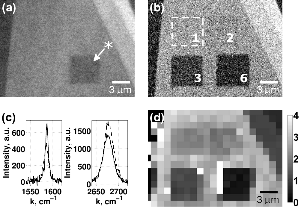
In order to understand the changes introduced in graphene by laser irradiation we use Raman spectroscopy. Figure 1 (c) shows Raman spectra of the point corresponding to the centre of the first modified region before (dashed) and after (solid) photomodification by 1 laser pulses for 1 minute. The G peak at 1580 originates from the doubly degenerate phonon mode at the Brillouin zone centre, while the 2D peak at 2700 corresponds to a double-resonance process, involving two transverse optical phonons near the K point. A symmetric 2D peak with a width of 25-45 is characteristic of monolayer graphene. Upon photoexcitation, the G peak is up-shifted by 1.2 and the 2D peak is down-shifted by 1.6 , and the intensity ratio of two peaks is decreased. Note that we have not observed the defect-induced D peak at 1350 , which indicates that photoexcitation does not induce structural defects. In Fig. 1 (d), we plot a Raman map of the intensity ratio of the 2D to G peaks for the flake. The photomodified square areas can be clearly seen, which indicates that modification is local, limited to the region of photoexcitation. Higher laser irradiation intensity gives rise to the stronger decrease of the intensity ratio, which corresponds to higher level of dopingDas et al. (2008).
It is well known that changes of the Raman 2D and G peak positions and intensities can be caused by both changes in doping and strain, and this bimodal sensitivity complicates data analysisDas et al. (2008); Mohiuddin et al. (2009); Ni et al. (2008); Zabel et al. (2012). However, this can be overcome by considering their correlated position. To get a qualitative description of the changes induced in graphene upon photoexcitation we apply the analysis first introduced in Ref. Lee et al., 2012b. This analysis is based on the fact that the fractional variation of peak positions is very different for cases of strain and doping. The average value of for uniaxial strain of random direction is 2.2, while for the carrier concentration above for the case of hole doping (i.e. a down-shift of the Fermi level) is approximately 0.7. Therefore contributions of strain and doping to the correlated peak position can be separated using vector decomposition with the gradient for unit vectors for strain- and doping-induced changes being 2.2 and 0.7, respectively. It should be noted that such a vector decomposition is more complicated for electron doping of graphene; however, our experiments on contacted graphene flakes revealed an increased level of hole (p) -doping as a result of photoexcitation. The origin for the correlated position plots, i.e. in Fig. 2 can be obtained from the results of Ref. Lee et al., 2012b using Raman peak dispersionFerrari et al. (2006) to take into account different Raman excitation wavelength, giving .
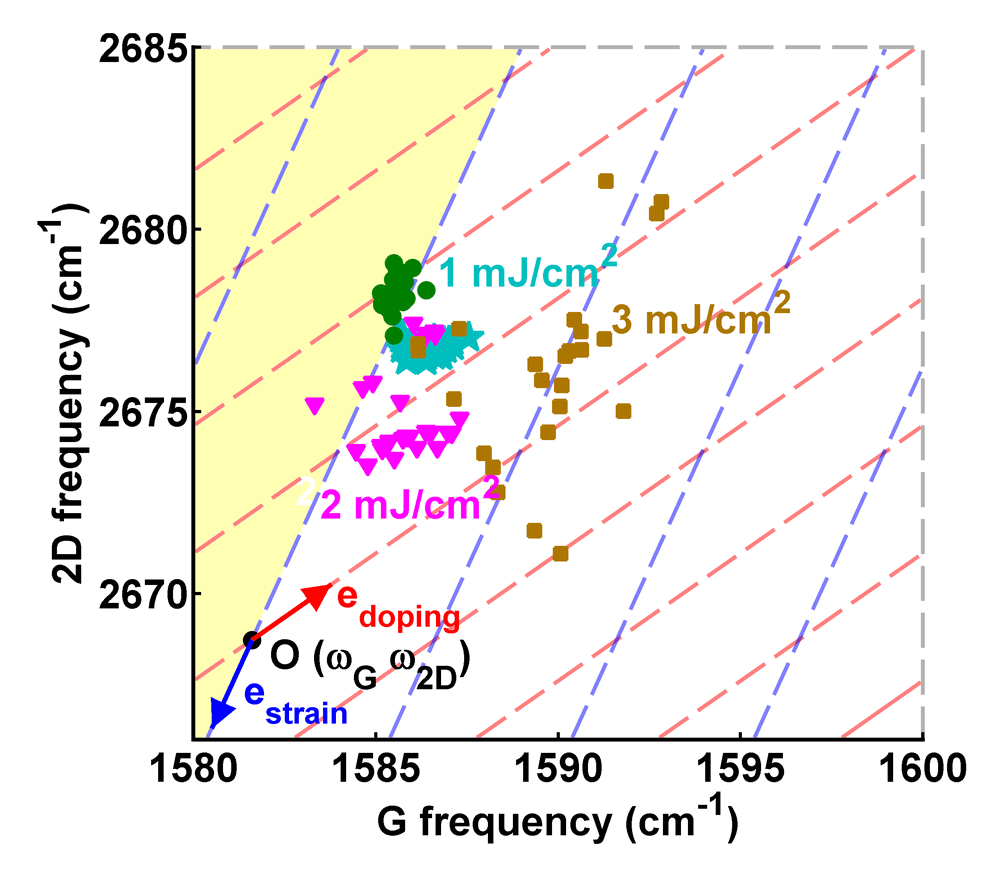
Figure 2 shows representative example of correlated peak position for different areas of the sample after photomodification using different laser fluences. Dashed blue (red) lines indicate direction of strain (doping) induced movement of the point for different constant values of strain (doping). The upshift (downshift) from the origin along ’strain’ lines corresponds to increasing compressive (tensile) strain. The upshift (downshift) along ’doping’ lines corresponds to increasing (decreasing) p-doping. The figure also shows origin (black dot) and unit vectors for doping (red) and strain (blue) induced peak shifts that can be used for vector decomposition. The yellow shaded region indicates a ’forbidden area’: since increasing doping leads to up-shift of the correlated peak position from the origin, can enter this area only for low levels of doping () when its dependence on Fermi level position becomes nonlinear. Since the native strain leads to non-negligible variation of , we need to take into account peak positions for the pristine sample. The green circle markers denote correlated peak position of non-modified sample. They form a narrow group with primarily strain-induced variation. However, the distribution changes dramatically after photomodification. After excitation with 1 (cyan stars) laser light the centre of distribution is shifted down and to the right hand side. To achieve this kind of movement, should be up-shifted along ’doping’ line and down-shifted along ’strain’ line. The former indicates the increase of the local doping level. The similar effect was observed in Ref. Luo et al., 2012 for UV excitation, where changes of the doping level were attributed to the photo-induced release of electron trapping adsorbate groups. The latter demonstrates that there is also a decrease in the strain level, i.e. photoexcitation is reducing the strain on the graphene. This is a remarkable effect, which has not been reported before. From Fig. 2 it can be seen that photoexcitation also leads to broadening of distribution which for 1 and 2 excitation is mostly caused by variation of doping and for 3 it is predominantly strain-induced.
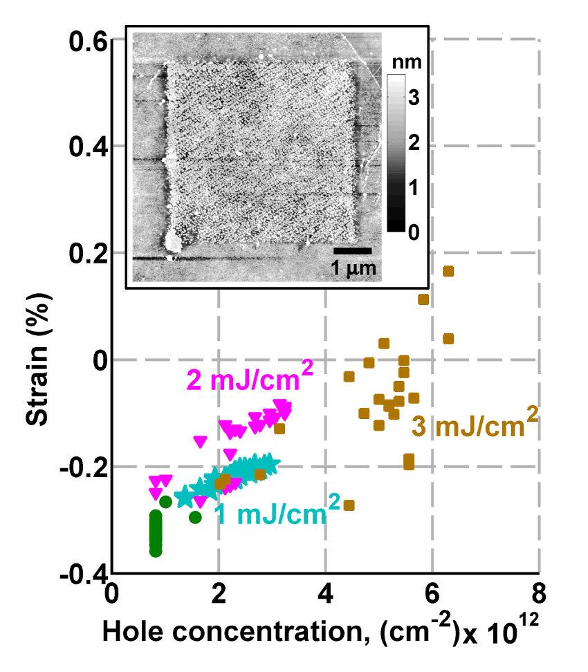
The non-orthogonal coordinate system, used in Fig. 2, complicates data interpretation. To clarify this, we can perform a vector decomposition to separate strain and doping contribution to the changes of the G peak position. We then use data from Refs. Das et al., 2008 and Ni et al., 2008 to obtain carrier concentration and strain levels which correspond to the observed G peak shifts. Note that for hole concentrations the linear approximation for doping-induced changes of is no longer valid, making vector decomposition and data fitting ambiguous. From Fig. 3 it can be seen that photomodification leads to both increasing level of p-doping and reduction of compressive strain; higher laser fluences cause larger changes in doping and strain.
We have observed slightly differing magnitudes and shifts in a number of graphene flakes, most likely depending on the starting strain of the flake, though this has proven difficult to correlate. While the magnitudes of changes per unit excitation fluence vary from sample to sample, the sign of the changes is predominantly the same, resulting in an increase in hole doping and a reduction in compressive strain. This behaviour has been observed in five different samples.
To conclude, we have investigated the modification of single layer graphene due to intense, picosecond near-infrared laser pulses. We find that photoexcitation leads to both a local increase of p-doping and reduction of compressive strain. With the short, intense laser pulses used in our experiments a number of mechanisms are feasible, including multi-photon excitation and non-equilibrium heating of the sample. The evidence from our experiments points towards enhanced atmospheric oxygen binding due to surface distortion, most likely caused by the rapid heating of the graphene. The inset of Fig. 3 shows an AFM image of one of the samples after modification, indicating the modified region has an increased surface roughness compared with surrounding non-modified areas. These changes are likely to be caused by slippage and buckling of the flake due to the mismatch in thermal expansion coefficients of graphene and underlying substrate. The doping level, meanwhile, can be explained by the enhanced bonding of atmospheric oxygen due to the distortion of graphene surfaceRyu et al. (2010). These effects are similar to the compressive strain and p-doping introduced in graphene upon annealingLee et al. (2012b); Ryu et al. (2010), though the different result, i.e. the reduction of compressive strain, may be explained by the very local nature of heating for our experiments.
Nevertheless, the local nature of the effects reported here could be utilized to create complex patterns that define device functionality, offering an advantage in spatial resolution and speed. However, to be able to change local properties of graphene in a controllable manner, more in-depth investigations to uncover the precise mechanisms at work are required.
References
- Wehling et al. (2008) T. O. Wehling, K. S. Novoselov, S. V. Morozov, E. E. Vdovin, M. I. Katsnelson, A. K. Geim, and A. I. Lichtenstein, Nano letters 8, 173 (2008).
- Wehling, Lichtenstein, and Katsnelson (2008) T. O. Wehling, A. I. Lichtenstein, and M. I. Katsnelson, Applied Physics Letters 93, 202110 (2008).
- Wang et al. (2010) Y. Wang, Y. Shao, D. W. Matson, J. Li, and Y. Lin, ACS Nano 4, 1790 (2010).
- Chen et al. (2007) W. Chen, S. Chen, D. C. Qi, X. Y. Gao, and A. T. S. Wee, Journal of the American Chemical Society 129, 10418 (2007).
- Robinson et al. (2010) J. T. Robinson, J. S. Burgess, C. E. Junkermeier, S. C. Badescu, T. L. Reinecke, F. K. Perkins, M. K. Zalalutdniov, J. W. Baldwin, J. C. Culbertson, and P. E. Sheehan, Nano letters 10, 3001 (2010).
- Teweldebrhan and Balandin (2009) D. Teweldebrhan and A. A. Balandin, Applied Physics Letters 94, 013101 (2009).
- Fischbein and Drndic (2008) M. D. Fischbein and M. Drndic, Applied Physics Letters 93, 113107 (2008).
- Withers et al. (2011) F. Withers, T. H. Bointon, M. Dubois, S. Russo, and M. F. Craciun, Nano letters 11, 3912 (2011).
- Sessi et al. (2009) P. Sessi, J. R. Guest, M. Bode, and N. P. Guisinger, Nano letters 9, 4343 (2009).
- Castro et al. (2007) E. V. Castro, K. Novoselov, S. Morozov, N. Peres, J. L. D. Santos, J. Nilsson, F. Guinea, A. Geim, and A. C. Neto, Physical review letters 99, 216802 (2007).
- Kane and Mele (2005) C. Kane and E. Mele, Physical review letters 95, 226801 (2005).
- McCann (2006) E. McCann, Physical Review B 74, 161403 (2006).
- Zhang et al. (2009) Y. Zhang, T.-T. Tang, C. Girit, Z. Hao, M. C. Martin, A. Zettl, M. F. Crommie, Y. R. Shen, and F. Wang, Nature 459, 820 (2009).
- Han et al. (2007) M. Y. Han, B. zyilmaz, Y. Zhang, and P. Kim, Physical review letters 98, 206805 (2007).
- Tapaszt et al. (2008) L. Tapaszt , G. Dobrik, P. Lambin, and L. P. Biro, Nature nanotechnology 3, 397 (2008).
- Stampfer et al. (2009) C. Stampfer, J. G ttinger, S. Hellm ller, F. Molitor, K. Ensslin, and T. Ihn, Physical review letters 102, 056403 (2009).
- Lemme et al. (2009) M. C. Lemme, D. C. Bell, J. R. Williams, L. A. Stern, B. W. Baugher, P. Jarillo-Herrero, and C. M. Marcus, ACS Nano 3, 2674 (2009).
- Hong and Jang (2012) J.-Y. Hong and J. Jang, Journal of Materials Chemistry 22, 8179 (2012).
- Li et al. (2008) X. Li, X. Wang, L. Zhang, S. Lee, and H. Dai, Science 319, 1229 (2008).
- Wang et al. (2008) X. Wang, Y. Ouyang, X. Li, H. Wang, J. Guo, and H. Dai, Physical review letters 100, 206803 (2008).
- Berger et al. (2004) C. Berger, Z. Song, T. Li, X. Li, A. Y. Ogbazghi, R. Feng, Z. Dai, A. N. Marchenkov, E. H. Conrad, and P. N. First, The Journal of Physical Chemistry B 108, 19912 (2004).
- Lin et al. (2011) Y.-M. Lin, A. Valdes-Garcia, S.-J. Han, D. B. Farmer, I. Meric, Y. Sun, Y. Wu, C. Dimitrakopoulos, A. Grill, and P. Avouris, Science 332, 1294 (2011).
- Luo et al. (2012) Z. Luo, N. J. Pinto, Y. Davila, and A. C. Johnson, Applied Physics Letters 100, 253108 (2012).
- Lee et al. (2012a) W. H. Lee, J. W. Suk, H. Chou, J. Lee, Y. Hao, Y. Wu, R. Piner, D. Akinwande, K. S. Kim, and R. S. Ruoff, Nano letters 12, 2374 (2012a).
- Stoehr et al. (2011) R. J. Stoehr, R. Kolesov, K. Xia, and J. r. Wrachtrup, ACS Nano 5, 5141 (2011).
- Gaskell et al. (2009) P. Gaskell, H. Skulason, C. Rodenchuk, and T. Szkopek, Applied Physics Letters 94, 143101 (2009).
- Ferrari et al. (2006) A. Ferrari, J. Meyer, V. Scardaci, C. Casiraghi, M. Lazzeri, F. Mauri, S. Piscanec, D. Jiang, K. Novoselov, and S. Roth, Physical review letters 97, 187401 (2006).
- Moger, Johnston, and Tyler (2008) J. Moger, B. D. Johnston, and C. R. Tyler, Optics express 16, 3408 (2008).
- Stoehr et al. (2010) R. J. Stoehr, R. Kolesov, J. Pflaum, and J. Wrachtrup, Physical Review B 82, 121408 (2010).
- Tielrooij et al. (2013) K. Tielrooij, J. Song, S. Jensen, A. Centeno, A. Pesquera, A. Z. Elorza, M. Bonn, L. Levitov, and F. Koppens, Nature Physics 9, 248 (2013).
- Jnawali et al. (2013) G. Jnawali, Y. Rao, H. Yan, and T. F. Heinz, Nano letters 13, 524 (2013).
- Currie et al. (2011) M. Currie, J. D. Caldwell, F. J. Bezares, J. Robinson, T. Anderson, H. Chun, and M. Tadjer, Applied Physics Letters 99, 211909 (2011).
- Hale et al. (2011) P. Hale, S. Hornett, J. Moger, D. Horsell, and E. Hendry, Physical Review B 83, 121404 (2011).
- Das et al. (2008) A. Das, S. Pisana, B. Chakraborty, S. Piscanec, S. Saha, U. Waghmare, K. Novoselov, H. Krishnamurthy, A. Geim, and A. Ferrari, Nature nanotechnology 3, 210 (2008).
- Mohiuddin et al. (2009) T. Mohiuddin, A. Lombardo, R. Nair, A. Bonetti, G. Savini, R. Jalil, N. Bonini, D. Basko, C. Galiotis, and N. Marzari, Physical Review B 79, 205433 (2009).
- Ni et al. (2008) Z. H. Ni, T. Yu, Y. H. Lu, Y. Y. Wang, Y. P. Feng, and Z. X. Shen, Acs Nano 2, 2301 (2008).
- Zabel et al. (2012) J. Zabel, R. R. Nair, A. Ott, T. Georgiou, A. K. Geim, K. S. Novoselov, and C. Casiraghi, Nano letters 12, 617 (2012).
- Lee et al. (2012b) J. E. Lee, G. Ahn, J. Shim, Y. S. Lee, and S. Ryu, Nature Communications 3, 1024 (2012b).
- Ryu et al. (2010) S. Ryu, L. Liu, S. Berciaud, Y.-J. Yu, H. Liu, P. Kim, G. W. Flynn, and L. E. Brus, Nano letters 10, 4944 (2010).