The effect of normal metal layers in ferromagnetic Josephson junctions
Abstract
Using the Usadel equation approach, we provide a compact formalism to calculate the critical current density of 21 different types of ferromagnetic (F) Josephson junctions containing insulating (I) and normal metal (N) layers in the weak link regions. In particular, we obtain that even a thin additional N layer may shift the - transitions to larger or smaller values of the thickness of the ferromagnet, depending on its conducting properties. For certain values of , a - transition can even be achieved by changing only the N layer thickness. We use our model to fit experimental data of SIFS and SINFS tunnel junctions, where S is a superconducting electrode.
pacs:
74.50.+r, 74.78.Fk, 74.45.+cI Introduction
The coexistence and competition of ferromagnetic and superconducting ordering leads to a rich spectrum of unusual physical phenomena, intensively studied during the recent years.Golubov et al. (2004); Buzdin (2005); Bergeret et al. (2005) One of the consequences is the so-called Josephson junction with phase shift in the ground state. This development makes the ferromagnetic Josephson junctions (FJJs) a subject of intensive theoretical and experimental studies.
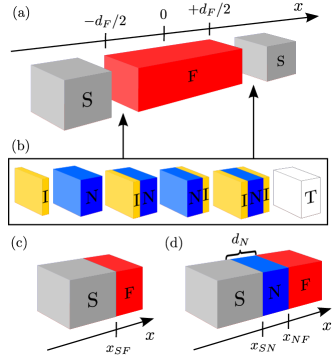
An FJJ usually contains two thick superconducting (S) electrodes with a ferromagnetic (F) film between them, see Fig. 1(a). In the present article we derive a formalism to calculate the critical current densities of FJJs with additional insulating (I) and normal metal (N) layers at the SF interfaces. A sign reversal of the critical current indicates a transition from the 0 to the state of the junction. This transition is usually realized by changing the thickness of the ferromagnet. However, we show that it can also be achieved by only changing the thickness of an N layer when inserted at the SF interface in SINF configuration.
The geometry of all FJJs we consider can be constructed by selecting one of the items of Fig. 1(b) and inserting it by following one of the arrows into Fig. 1(a). At the other arrow position we insert either the same or another item from Fig. 1(b). In this way we obtain 21 possible FJJ configurations.
The purpose of the additional I layer(s) is to enlarge the product in the -state. Here is the critical current density of the junction and is its normal resistance, which is mainly determined by the insulating barrier(s).
One reason why we consider additional N layers is the existence of a so-called “dead” layer which is assumed in order to fit many experiments.Oboznov et al. (2006); Blum et al. (2002); Sellier et al. (2003); Weides et al. (2006a, b); Pfeiffer et al. (2008); Bannykh et al. (2009) This dead layer is a part of the ferromagnet which behaves as a nonmagnetic metal. It usually appears due to the surface roughness or the mutual dissolution of N and F layers. It is inherent for example for Cu, which is very popular as a spacer, and its alloys with 3d metals. Usually it is assumed that the dead layer makes the effective F layer thinner. However, does the dead layer cause additional effects, and at what conditions? Our calculations aim to answer this question.
The answer to this question is also important for the development of magnetic memory cells for rapid single flux quantum (RSFQ) logics which becomes more and more actual.Goldobin et al. (2013); Abd El Qader et al. (2014); Robinson et al. (2014); Niedzielski et al. (2014); Alidoust and Halterman (2014); Baek et al. (2014); Iovan et al. (2014) Only recently, a new type of magnetic memory element based on FJJs with a complex insulator-superconductor-ferromagnet weak link (SIsFS) was proposed.Bakurskiy et al. (2013); Larkin et al. (2012) These FJJs have a large product in the -phase. The middle superconducting “s” layer is inserted in the weak link to recover the superconducting pairing and increase . The thickness of this layer is of the order of the coherence length so that it may make a transition to the normal state at different conditions than the thick outer S electrodes. One of the aims of our calculation is to study the behavior of such SIsFS FJJs when their middle superconducting layer is in the normal state.
Ferromagnetic Josephson junctions can also be used as (non-dischargeable) on-chip -phase batteries for self-biasing various electronic circuits in classical and quantum domains, e.g. self-biased RSFQ logicOrtlepp et al. (2006) or flux qubits.Ioffe et al. (1999); Klenov et al. (2008); Yamashita et al. (2006) In classical circuits, a phase battery may also substitute the conventional inductance and substantially reduce the size of an elementary cell.Ustinov and Kaplunenko (2003) Some of these proposals were already realized practically.Ortlepp et al. (2006); Feofanov et al. (2010) The key question for their realization is the range of parameters, e.g. the ferromagnetic layer thickness , at which the ground state is established, that is, the - transition occurs. In recent works Vasenko et al. (2008); Buzdin (2003) it was shown that the presence of extra insulating layers shifts the first - transition to smaller values of . The explanation of this effect is that the order parameter decreases step-wise at the I barrier(s) so that one requires a thinner F layer to reach the - transition.
Introducing an N layer between the ferromagnet and the S electrode was technologically necessary in many FJJ experiments.Ryazanov et al. (2001); Oboznov et al. (2006); Blum et al. (2002); Sellier et al. (2003); Born et al. (2006); Weides et al. (2006a, b); Pfeiffer et al. (2008); Robinson et al. (2006, 2007); Wild et al. (2010) However, such a situation was not taken into account by any theoretical explanation of these experiments, or considered in previous theoretical works on tunnel FJJs both in the clean and dirty limits,Golubov et al. (2002); Golubov and Yu. Kupriyanov (2005); Pugach et al. (2009); Jun-Feng Liu and Chan (2010); Vasenko et al. (2010, 2011) see Refs. Buzdin, 2005; Golubov et al., 2004 for review. As we show in the current paper, this is only reasonable if the F and N metals behave fully identically, except for their magnetic properties. Otherwise, the presence of a thin N layer changes the boundary conditions which influences, in particular, the dependence of the Josephson current density on the F layer thickness . Recent experiments,Ryazanov et al. (2008) which use a new continuous in-situ technology allowing the deletion of this layer, exhibit actually a change of the - transitions in the dependence.
The article is organized as follows. In Sec. II we describe our model based on the Usadel equations supplemented with Kupriyanov-Lukichev boundary conditions. Different types of interlayer boundaries are analyzed. Section III presents the obtained dependencies of the critical current density on the F layer thickness as well as the analysis of the - transitions in the framework of a linear approximation. We use our formalism in Sec. IV to fit experimental data of SINFS and SIFS junctions. Section V concludes this work. Details of the calculation can be found in the appendix.
II Model
II.1 The boundary value problem
The basic Josephson junction configuration we consider is sketched in Fig. 1(a). It consists of two thick S electrodes enclosing an F layer of the thickness along the axis. Our model allows to consider an additional I or N layer at the SF interfaces as well as I layers at the SN or NF interfaces, as illustrated by Fig. 1(b).
We calculate the critical current density of these configurations by determining their Green’s functions in the “dirty” limit. In this limit, the elastic electron scattering length is much smaller than the characteristic decay length of the superconducting wave function. We determine the Green’s functions with the help of the Usadel equations, Usadel (1970) which we use similar to Ref. Buzdin, 2005 in the form
| (1) |
in the N and F layer, where and are the Usadel Green’s functions, while . The frequencies contain the scaled Matsubara frequencies , where at the temperature , and is the critical temperature of the superconductor. By using the definition we take, similar to Ref. Vasenko et al., 2008, the spin-flip scattering time into account. This approach requires a ferromagnet with strong uniaxial anisotropy like for example Cu alloys with transition metals, which are used in many experiments. Equation (1) should be satisfied for any integer number . The scaled exchange energy of the ferromagnetic material, where the energy describes the exchange integral of the conducting electrons, is assumed to be zero in the N layer.
In our model we use the coherence lengths
| (2) |
of the superconducting correlations, which are defined with the help of the diffusion coefficients and in the normal and ferromagnetic metal, respectively. We use the scaling defined by .
The decay length of superconducting correlations in the ferromagnet is usually in the order of nm. Therefore this is sufficiently small () to consider the supercurrent as a result of interference of anomalous Green’s functions induced from the superconducting banks. It is convenient to consider this problem in theta parametrizationZaikin and Zharkov (1981)
| (3) |
where is independent of the coordinate . It corresponds to the phase of the order parameter of the S banks for the right and left superconducting electrode respectively, while satisfies the sine-Gordon type differential equation
| (4) |
Since we assume that the superconductivity in the S electrodes is not suppressed by the neighboring N and F layers, we obtain
| (5) |
analogous to Vasenko et al.Vasenko et al. (2008) at the interfaces of the superconductor, where is the absolute value of the order parameter in the superconductor. The validity of this assumption depends on the values of the suppression parameters
| (6) |
at the S boundaries, which we discuss in more detail in Subsec. II.3. Here we use the resistances , and the areas , of the SN and SF interfaces. The values , and describe the resistivity of the N, F, and S metals, respectively.
The Kupriyanov-Lukichev boundary condition Yu. Kuprianov and Lukichev (1988); Koshina and Krivoruchko (2000) at the superconducting interface, shown in Fig. 1(c), is
| (7) |
where , while in Fig. 1(d) it is
| (8) |
where , at the SN boundary and
| (9) |
at the NF boundary. Here we defined and . Additionally we use the differentiability condition
| (10) |
The suppression parameters
| (11) |
are defined analogous to Eq. (6), but not restricted to only small or large values.
In order to finally extract the critical current density from the current phase relation we will calculate the total current density Golubov et al. (2004)
| (12) |
flowing through our device, with the help of the Green’s function in the F layer. Here we chose the position , see Fig. 1(a), in order to simplify the calculation.
II.2 Critical current density
In this section we rewrite expression (12) to be able to directly calculate the critical current densities of all SFS Josephson junctions of the type sketched in Fig. 1(a), which may include each one of the layers shown in Fig. 1(b) at the SF interfaces.
In order to solve the Usadel equations (1) in the F layer we use the ansatz Buzdin and Yu. Kupriyanov (1991); Vasenko et al. (2008)
| (13) |
where each function and solves the non-linear differential equation (4) for . Additionally we use the conditions and at . Then the solution will turn out to be most dominant in the left side of the F part and to decay exponentially in the right side of the junction. Therefore, it has practically no overlap with the solution which is dominant in the right side of the F layer. It was shown Vasenko et al. (2008) that this ansatz is valid even for small distances , that is, in the region of the first - transition, where is defined by Eq. (2).
We obtain both solutions and by integrating the differential equation (4) for twice. The first integration results in
| (14) |
where . A second integration leads us by using the definition to the equationVasenko et al. (2008); Fauré et al. (2006)
| (15) |
Here are the integration constants. In the F layer we can assume small superconducting correlations to linearize the denominator of the left-hand side of Eq. (15) which leads us to the equation
| (16) |
The rewritten integration constants are given by the boundary conditions at the right and left ferromagnetic interfaces as
| (17) |
II.3 SF interface without or including an N layer
In the following we determine a constant to replace or in Eq. (18) in the case of no N layer at an SF interface, as shown for example in Fig. 1(c). The index TI stands for transparent or insulating.
We insert the integrated sine-Gordon equation (14) at the position into the boundary condition (7) and obtain the relation
| (19) |
By defining analogous to Eq. (17) we rewrite Eq. (19) in the form
| (20) |
In the case , this equation is a quartic equation in and therefore exactly solvable. To find the solutions in this case we use the function solve of the software MATLAB. Afterwards we make use of Eq. (19) to select one of the four solutions. In the case we solve Eq. (20) numerically by using the function fsolve of the software MATLAB together with the solution of the limit as starting value.
In this way we find for the determination of the critical current density (18) in the case of no N layer at the SF boundary. The case of a small parameter corresponds to a transparent SF interface, while a large one corresponds to an insulating interface.Vasenko et al. (2008); Fauré et al. (2006)
Next we determine a constant for the case of a thin N layer between the superconductor and ferromagnet as shown in Fig. 1(d).
By inserting the integrated sine-Gordon equation (14) for into the boundary condition (9) we obtain the equation
| (21) |
When we rewrite this equation using the definition , the result
| (22) |
looks similar to Eq. (20). The main difference is that it reduces in the case not to an equation of fourth order in . This is because we take the inverse proximity effect at the NF boundary into account. Therefore, the value depends also on , which itself is related to , even in the case , as we show in the appendix.
However, we also show in the appendix that Eq. (22) reduces in the limit together with to an equation of fourth order in . Therefore, we make three steps in order to solve Eq. (22). First we determine its solution in the case similar to the forth-order case of Eq. (20). We then use this result as a starting value to solve Eq. (22) for only the limit with the help of the function fsolve of the software MATLAB. This in turn leads to another starting value which we use to solve Eq. (22) with fsolve, but without any limiting case.
The solution of Eq. (22) finally can be used as or for the determination of the critical current density (18) in the case of an N layer at the SF interfaces. Small parameters and correspond to transparent SN and NF interfaces, while large ones correspond to insulating interfaces.Vasenko et al. (2008); Fauré et al. (2006)
III Discussion
In this section we first select FJJ configurations, where the N layer has the largest influence. We then analyze their critical current densities with the help of the formalism we derived in the previous section. Finally we discuss the results with the help of solutions of the linearized differential equation (4).
We do not analyze configurations, where a thin N layer () is located between S and I layers, which gives only a negligible reduction of compared to the case without an N layer. This is because the superconducting condensate just penetrates into the whole N layer. The same effect occurs when the thin N spacer separates the S and F layers and both (SN and NF) interfaces are transparent.
However, when the SN boundary has a very weak transparency or gets even insulating, that is, the N layer is located between an I and F layer, then the N layer(s) play(s) a more notable role depending on the relation of resistances (11), as we will see in the following.
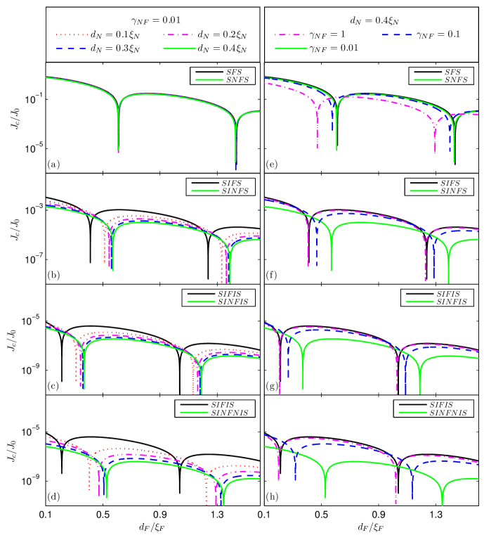
Examples for the critical current density in these situations are presented in Fig. 2 with different numbers of insulating barriers. To in- and exclude these barriers we use the boundary parameters shown in Tab. 1. Since we only want to change N-layer properties, like , or of the same junction, we keep the product
| (23) |
constant.
Each figure 2(a-d) shows several dependences for FJJs containing N layers of different thicknesses and the corresponding reference FJJ without any N layer (solid black linesVasenko et al. (2008); Buzdin and Baladié (2003)). The I layers in all panels of Fig. 2(b-d,f-h) are chosen to be exactly identical. Here we observe that the additional N layer at the IF boundary decreases the amplitude of by 1–2 orders of magnitude and, while the insulating barrier at the SF boundary shifts the - transitions towards smaller values of (solid black lines), the additional N layer in the SINF part shifts it back to larger .
This effect depends strongly on the value , as can be seen from Figs. 2(f-h), where we show critical current densities in the same FJJ configurations as in Figs. 2(b-d), but with fixed and variable . With decreasing , the - transitions get more shifted back to their positions without I layer. One may conclude that the thin N layer with small resistance () effectively “smooths” the order parameter in the SIF region.
For a physical explanation of this behavior one can imagine that a decrease of the amplitude of the superconducting pair wave-function in the F layer is connected to a decrease of the function . In particular, the positions along the F layer where becomes zero correspond to sign reversals of the critical current and are therefore directly linked to the thicknesses where a - transition occurs.
| Interface | Eq. for | |||
|---|---|---|---|---|
| SF | 0.001 | – | – | (20) |
| SIF | 100 | – | – | (20) |
| SNF | – | 0.001 | 0.001 | (22) |
| SINF | – | 0.001 | 100 | (22) |
This picture already helped to understand why an insulating layer at the SF interface shifts the - transitions towards smaller values of .Vasenko et al. (2008); Buzdin (2003) This is because the I layer induces a decreasing shift to at the SF interface, as can be seen from Eq. (7) for . Since decreases monotonically from the interfaces into the F layer, this shift results in a shift of its zeros towards the interface. This in turn leads to a shift of the - transitions to smaller , as can be seen by comparing e.g. the black lines in Figs. 2(a) and 2(b).
By inserting an N layer at the IF interface we can mitigate this effect. In fact, the function gets still decreased by the I layer, but the decrease of its derivative may be less than compared to the case when the superconducting pair wave-function directly penetrates the F layer. This in turn leads to a shift of the - transition back to larger .
To explain this effect we replace the derivative in Eq. (43) with the help of Eq. (10) which leads us to the derivative
| (24) |
at the F interface. For , Eq. (24) resembles Eq. (7). Therefore we obtain, by using the values defined in Tab. 1, the correct limiting results.
An increase of increases and therefore shifts the - transitions towards larger , as shown by Figs. 2(b–d). Furthermore, from Eq. (24) can be understood why a smaller value of induces a larger increase of . This again shifts the - transitions towards larger , as shown by Figs. 2(f–h).
The same effect occurs in Fig. 2(e), but it has a different interpretation because the - transitions are already shifted to large without an N layer, due to the absence of the I layer (black line). A small value of does not change this situation significantly. However, if increases and therefore decreases, the - transitions get shifted to smaller .
Note that these effects are related not only to the thickness of the N layer that may be small () but mainly to its conducting properties represented by (11).
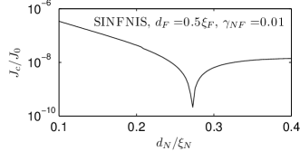
The influence of N layers on FJJs can be seen most clearly when they are inserted at IF interfaces and is kept constant not far from a 0- transition while changes. In this way, the - transition can be controlled by , as shown in Fig. 3. Here we consider an SIFIS junction which is in the state for . By adding N layers at the IF interfaces and increasing their thicknesses simultaneously, we tune the FJJ into the regime. Figure 3 considers the same FJJ configuration as Fig. 2(d), where is fixed and changes.
To understand the role of the boundary parameters in the - transition patterns in more detail, it is useful to analyze it in a simple linear approximation. This approximation can be used if both S electrodes have nontransparent interfaces, or if . Then we may assume that , , and . The general solution of the Usadel equations (1) in the non-superconducting layers has the form , where , , where and are real. The critical current density is given by the expression (12). For FJJs without N layer, the critical current density was already calculated in Refs. Vasenko et al., 2008; Buzdin and Baladié, 2003; Fauré et al., 2006; Vasenko et al., 2011.
III.0.1 Transparent-interface structures: SFS, SNFS, SNFNS
We start with the analysis of Figs. 2(a) and 2(e). For this purpose we assume that all interfaces are transparent, that is and If , the critical current density of the SFS junction (cf. solid black lines) readsBuzdin (2005)
| (25) |
and the positions of the - transitions are defined by the solutions of the equation
| (26) |
This gives , and the first - transition occurs at . For a large exchange energy , we obtain and . When we assume , the first - transition occurs at , that is , which is in good agreement with Figs. 2(a) and 2(e).
By adding normal layers in the case of , we see that even for two extra layers in the SNFNS configuration, the critical current density
| (27) |
differs not much from Eq. (25). We only obtain an additional real factor , but the position of the - transitions is still defined by the term marked as real part. Therefore, the positions of the - transitions will be the same as in the SFS case, see Fig. 2(a) for one extra N layer. The small boundary parameter is needed in order to neglect the proximity effect in the S electrodes.
However, if in the SNFS junction (dashed-dotted line in Fig. 2(e)), the electrons may easily change between the N and F layers, since . Therefore, the Josephson phase drops partially along the N layer and the first - transition shifts towards smaller values of .
III.0.2 Double-barrier structures SIFIS vs. SINFNIS
In order to discuss the interplay of the N and I layers we jump to the description of the configurations shown by Figs. 2(d) and 2(h). Here the resistance of the insulating barriers is large but the NF boundaries are still transparent and we do not need any assumption about the temperature to use the linear approximation.
The critical current density of the SIFIS junction (cf. solid black lines) at is
| (28) |
The points of the - transitions are now defined by the solutions of the equation
| (29) |
Here the assumption yields only . At a large exchange energy the first - transition occurs at , that is , which is in agreement with Figs. 2(d) and 2(h). Its exact position is defined by the factor as well as Buzdin and Baladié (2003) .
In the case of intermediate resistances of the SF interfaces of an SFS JJBuzdin (2005), the critical current density reads
| (30) |
which transforms into the two previous cases (25) and (28) for and , respectively. The points of the - transitions are defined by
| (31) |
If , that is , the first - transition is located in the range If , it occurs at
In contrast, the critical current density of the SINFNIS junction at at transparent NF interfaces and , has the form
| (32) |
The - transitions are defined by the zeros of the real part, which has the same form as in the case of SFS JJs with transparent interfaces (25). That is, the N layers have mitigated the effect of the I layers, which can be seen by comparing Fig. 2(d) with Fig. 2(a).
III.0.3 SIFIS vs. SINFIS structures
The effect of a single N layer on a double-barrier SIFIS junction, shown in Figs. 2(c) and 2(g), is discussed in the following. The critical current density of the SINFIS junction with the same boundary parameters as in the section before is given by
| (33) |
In this case the - transitions are defined by the zeros of the function and located at the positions where , that is they are also shifted towards larger in comparison with the ones of the SIFIS junction, see Figs. 2(c) and 2(g).
In our previous articlePugach et al. (2009) we obtained in fact the same expressions (28) and (33). There we assumed that the interface transparencies of both S electrodes are small, one of them due to the presence of an insulating barrier. In this way we analyzed SI1FI2S and SI1NFI2S structures with rather different transparencies of the I1 and I2 barriers. We found in the linear approximation that the critical current density for an SI1NFI2S FJJ is the same as the one for an SI1FNI2S structure.
III.0.4 SIFS vs. SINFS structures
If the structure contains only one insulating barrier, as in Figs. 2(b) and 2(f), we may use the tunnel Hamiltonian method, which yields for the critical current density the expression
| (34) |
To use the linear approximation we shall assume that is close to , and in order to neglect the proximity effect in the right S electrode we use the rigid boundary conditions We also assume the N layer to be thin . Then we obtain
| (35) |
To find the position of the first - transition we assume and neglect , because the last value is determined by the large resistance of the I barrier. The solution weakly depends on because the suppression of the superconducting correlation along the thin N layer is negligible in comparison with the one of the I barrier. However, the ratio of the N and F resistance, which defines via the derivative jump (10) at the NF interface, still plays a role. Then the - transition takes place at , for which the equation
| (36) |
is satisfied.
IV Comparison with experiment
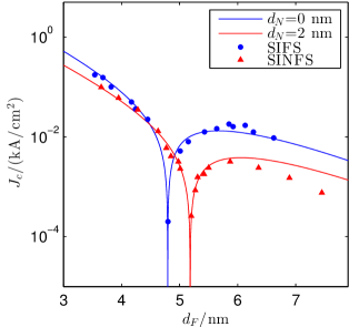
To check our theory, we use data of SINFS experiments performed by M. Weides et al.Weides et al. (2006a) on Nb/Al2O3/Cu/Ni0.6Cu0.4/Nb FJJs. The samples used in these experiments include a 2 nm Cu interlayer between the I and F layer. Using the same technology, new series of samples were produced, but the process was changed in order to delete the Cu layer. That is, we can compare SIFS and SINFS FJJs with the same layer properties including the concentration of the NiCu alloy. In Fig. 4 we show a fit of experimental data of critical current densities for different F layer thicknesses of both types of junctions. Dots correspond to SIFS junctions and triangles correspond to SINFS junctions.
We calculated the critical currents with the help of Eq. (18). In the case of the SIFS configuration we made use of Eq. (20) to calculate the parameter and in the case of the SINFS configuration we used Eq. (22).
For our fit we used the coherence lengths =10 nm, =7.60 nm and =1.72 nm. Our exchange energy =880 is situated between the value 850 corresponding to the alloy Ni0.53Cu0.47Ryazanov et al. (2001) and the value 930 of clean Ni.Robinson et al. (2006) The product =1/1.7 is similar to the one used by Weides et al.Weides et al. (2006a) Further values taken from this publication are the temperature T=4.2 K, junction area =(100 µm)2 and resistivity =54 µcm. Additionally we used the damped critical temperature Tc=7.2 K ̵͑of Nb and the resistivity =0.66 µcm.
As we have shown in Fig. 2(f), a small suppression parameter results in a shift of the 0- transition to larger for the sample with N layer. This effect explains the shift of the - transition observed in the experiments on SIFS and SINFS FJJs. The difference in the amplitude of the curves is attributed to the different thickness of the I barrier in these two sample series.
This conclusion is supported by preliminary experimental observations on SIsFS junctions. These observations indicate that the introduction of a thin s interlayer, which should make a transition to the normal state if its thickness is of the order of the coherence length, shifts the - transitions towards larger dF.
V Conclusion
Using the Usadel equations we have calculated the critical current density of ferromagnetic Josephson junctions (FJJs) of different types, containing I and N layers at the SF interfaces and compared it to critical current densities of structures without N layers. Such layers were technologically required in many FJJ experiments, but were not taken into account in previous models.
It was shown earlier Vasenko et al. (2008); Buzdin and Baladié (2003); Fauré et al. (2006) that insulating barriers decrease the critical current density and shift the - transitions to smaller values of the ferromagnet thickness . A thin N layer inserted between S and I layers does not significantly influence the Josephson effect. However, if the N layer is inserted between I and F layers, it can have a large effect on the curve. If additionally the transport properties of the F and N layers differ significantly (), the presence of the N layer shifts the first - transition to larger , see Figs. 2(b-d). At certain values of , the 0- transition can even be achieved by changing only , see Fig. 3. Finally, our theory allows the explanation of experimental data for SINFS and SIFS junctions, shown in Fig. 4.
The oscillation period of is still determined by the relation of the magnetic exchange energy and the diffusion coefficient in the dirty limit. At an average scattering strength this is in general not valid.Pugach et al. (2011) If the transport properties of the N layer between the I and F layer are the same as those of the ferromagnet, the dependence does not change. This means in particular, that the dead layerOboznov et al. (2006); Blum et al. (2002); Sellier et al. (2003); Weides et al. (2006a, b); Pfeiffer et al. (2008); Bannykh et al. (2009) plays only a role if its properties differ from the ones of the ferromagnet, not only in terms of the absence of ferromagnetism, but also in terms of its resistance. The smaller the value of , the larger is the change of the amplitude and the shift of the - transitions, see Figs. 2(f-h).
The situation is completely different in the case of transparent SF interfaces, that is without an I layer in between. In this case the additional thin normal layer with conductivity much larger than the one of the ferromagnet () does not play any role. In the same setup, an N layer with transport properties similar to the ones of the ferromagnet () provides a shift of the - transition to smaller , see Fig. 2(e). This process is explained in more detail after Eq. (24).
In summary, even a thin additional N layer may change the boundary conditions at the IF boundary depending on the value of . We conclude that it can effectively mitigate the effect of the insulating barrier on the decaying oscillations of the critical current density . Even technological thin N layers, which almost do not suppress the superconducting correlations, have to be taken into account for the explanation of experimental results concerning the Josephson effect in FJJs.
Acknowledgements.
We thank Prof. V. V. Ryazanov for fruitful and stimulating discussions, N. G. P. thanks the CMPC RHUL for giving new ideas in stimulating discussions, and D. M. H. thanks Prof. W. P. Schleich and K. Vogel for giving him the possibility to work at the Lomonosov Moscow State University. Financial support by the DFG (Projects SFB/TRR-21 and KO 1953/11-1), the EPSRC (grant no. EP/J010618/1), the Russian Foundation for Basic Researches (RFBR grant no. 13-02-01452-a, 14-02-90018-Bel-a), and the Ministry of Education and Science of Russian Federation (grant no. 14Y26.31.0007) is gratefully acknowledged. *Appendix A N layer Green’s function
In this appendix we first show how to find the dependence of on in order be able to solve Eq. (22) numerically for . Thereafter we reduce Eq. (22) in the limiting case to an equation of fourth order in .
We start by solving the Usadel equation (4) in the case , that is
| (37) |
where because the exchange energy is zero in the N layer.
When we assume , the function changes only slowly. Therefore, we make in the right-hand side of Eq. (37) the approximation
| (38) |
where . Note that we cannot neglect this term because may be of the order of , depending on the boundary parameters. The solution of Eq. (37) using the approximation (38) reads
| (39) |
Inserting the constant
| (40) |
determined from the the boundary condition (8) at the SN interface, into the Green’s function (39) at the position connects the NF boundary value
| (41) |
to the SN boundary value , which we determine in the next step.
For this purpose we use the integrated sine-Gordon equation (14) at the position and insert it into the differentiability condition (10) to obtain
| (42) |
Here we replace the right-hand side by the derivative
| (43) |
of the function from Eq. (39).
These steps lead us with the definition to
| (44) |
This equation can be written as an equation of second order in and can therefore be solved exactly for . Inserting the result into Eq. (41) gives us as a function of which itself, when inserted into Eq. (22), allows us to determine finally by solving the transcendental equation (22) numerically.
References
- Golubov et al. (2004) A. A. Golubov, M. Yu. Kupriyanov, and E. Il’ichev, Rev. Mod. Phys. 76, 411 (2004).
- Buzdin (2005) A. I. Buzdin, Rev. Mod. Phys. 77, 935 (2005).
- Bergeret et al. (2005) F. S. Bergeret, A. F. Volkov, and K. B. Efetov, Rev. Mod. Phys. 77, 1321 (2005).
- Oboznov et al. (2006) V. A. Oboznov, V. V. Bol’ginov, A. K. Feofanov, V. V. Ryazanov, and A. I. Buzdin, Phys. Rev. Lett. 96, 197003 (2006).
- Blum et al. (2002) Y. Blum, A. Tsukernik, M. Karpovski, and A. Palevski, Phys. Rev. Lett. 89, 187004 (2002).
- Sellier et al. (2003) H. Sellier, C. Baraduc, F. Lefloch, and R. Calemczuk, Phys. Rev. B 68, 054531 (2003).
- Weides et al. (2006a) M. Weides, M. Kemmler, E. Goldobin, D. Koelle, R. Kleiner, H. Kohlstedt, and A. Buzdin, Appl. Phys. Lett. 89, 122511 (2006a).
- Weides et al. (2006b) M. Weides, M. Kemmler, H. Kohlstedt, R. Waser, D. Koelle, R. Kleiner, and E. Goldobin, Phys. Rev. Lett. 97, 247001 (2006b).
- Pfeiffer et al. (2008) J. Pfeiffer, M. Kemmler, D. Koelle, R. Kleiner, E. Goldobin, M. Weides, A. K. Feofanov, J. Lisenfeld, and A. V. Ustinov, Phys. Rev. B 77, 214506 (2008).
- Bannykh et al. (2009) A. A. Bannykh, J. Pfeiffer, V. S. Stolyarov, I. E. Batov, V. V. Ryazanov, and M. Weides, Phys. Rev. B 79, 054501 (2009).
- Goldobin et al. (2013) E. Goldobin, H. Sickinger, M. Weides, N. Ruppelt, H. Kohlstedt, R. Kleiner, and D. Koelle, Appl. Phys. Lett. 102, 242602 (2013).
- Abd El Qader et al. (2014) M. Abd El Qader, R. K. Singh, S. N. Galvin, L. Yu, J. M. Rowell, and N. Newman, Appl. Phys. Lett. 104, 022602 (2014).
- Robinson et al. (2014) J. W. A. Robinson, N. Banerjee, and M. G. Blamire, Phys. Rev. B 89, 104505 (2014).
- Niedzielski et al. (2014) B. M. Niedzielski, S. G. Diesch, E. C. Gingrich, Yixing Wang, R. Loloee, W. P. Pratt, and N. O. Birge, IEEE Trans. Appl. Supercond. 24, 1 (2014).
- Alidoust and Halterman (2014) M. Alidoust and K. Halterman, Phys. Rev. B 89, 195111 (2014).
- Baek et al. (2014) B. Baek, W. H. Rippard, S. P. Benz, S. E. Russek, and P. D. Dresselhaus, Nat. Commun. 5, 3888 (2014).
- Iovan et al. (2014) A. Iovan, T. Golod, and V. M. Krasnov, “Controllable generation of a spin-triplet supercurrent in a Josephson spin-valve,” (2014), arXiv:1405.4754 .
- Bakurskiy et al. (2013) S. V. Bakurskiy, N. V. Klenov, I. I. Soloviev, V. V. Bol’ginov, V. V. Ryazanov, I. V. Vernik, O. A. Mukhanov, M. Yu. Kupriyanov, and A. A. Golubov, Appl. Phys. Lett. 102, 192603 (2013).
- Larkin et al. (2012) T. I. Larkin, V. V. Bol’ginov, V. S. Stolyarov, V. V. Ryazanov, I. V. Vernik, S. K. Tolpygo, and O. A. Mukhanov, Appl. Phys. Lett. 100, 222601 (2012).
- Ortlepp et al. (2006) T. Ortlepp, Ariando, O. Mielke, C. J. M. Verwijs, K. F. K. Foo, H. Rogalla, F. H. Uhlmann, and H. Hilgenkamp, Science 312, 1495 (2006).
- Ioffe et al. (1999) L. B. Ioffe, V. B. Geshkenbein, M. V. Feigel’man, A. L. Fauchère, and G. Blatter, Nature 398, 679 (1999).
- Klenov et al. (2008) N. Klenov, V. Kornev, A. Vedyayev, N. Ryzhanova, N. Pugach, and T. Rumyantseva, J. Phys. Conf. Ser. 97, 012037 (2008).
- Yamashita et al. (2006) T. Yamashita, S. Takahashi, and S. Maekawa, Appl. Phys. Lett. 88, 132501 (2006).
- Ustinov and Kaplunenko (2003) A. V. Ustinov and V. K. Kaplunenko, J. Appl. Phys. 94, 5405 (2003).
- Feofanov et al. (2010) A. K. Feofanov, V. A. Oboznov, V. V. Bol’ginov, J. Lisenfeld, S. Poletto, V. V. Ryazanov, A. N. Rossolenko, M. Khabipov, D. Balashov, A. B. Zorin, P. N. Dmitriev, V. P. Koshelets, and A. V. Ustinov, Nat. Phys. 6, 593 (2010).
- Vasenko et al. (2008) A. S. Vasenko, A. A. Golubov, M. Yu. Kupriyanov, and M. Weides, Phys. Rev. B 77, 134507 (2008).
- Buzdin (2003) A. Buzdin, Pis’ma Zh. Eksp. Teor. Fiz. 78, 1073 (2003), [JETP Lett. 78, 1073 (2003)].
- Ryazanov et al. (2001) V. V. Ryazanov, V. A. Oboznov, A. Yu. Rusanov, A. V. Veretennikov, A. A. Golubov, and J. Aarts, Phys. Rev. Lett. 86, 2427 (2001).
- Born et al. (2006) F. Born, M. Siegel, E. K. Hollmann, H. Braak, A. A. Golubov, D. Yu. Gusakova, and M. Yu. Kupriyanov, Phys. Rev. B 74, 140501 (2006).
- Robinson et al. (2006) J. W. A. Robinson, S. Piano, G. Burnell, C. Bell, and M. G. Blamire, Phys. Rev. Lett. 97, 177003 (2006).
- Robinson et al. (2007) J. W. A. Robinson, S. Piano, G. Burnell, C. Bell, and M. G. Blamire, Phys. Rev. B 76, 094522 (2007).
- Wild et al. (2010) G. Wild, C. Probst, A. Marx, and R. Gross, Eur. Phys. J. B 78, 509 (2010).
- Golubov et al. (2002) A. A. Golubov, M. Yu. Kupriyanov, and Ya. V. Fominov, Pis’ma Zh. Eksp. Teor. Fiz. 75, 223 (2002), [JETP Lett. 75, 190 (2002)].
- Golubov and Yu. Kupriyanov (2005) A. A. Golubov and M. Yu. Kupriyanov, Pis’ma Zh. Eksp. Teor. Fiz. 81, 419 (2005), [JETP Lett. 81, 335 (2005)].
- Pugach et al. (2009) N. G. Pugach, M. Yu. Kupriyanov, A. V. Vedyayev, C. Lacroix, E. Goldobin, D. Koelle, R. Kleiner, and A. S. Sidorenko, Phys. Rev. B 80, 134516 (2009).
- Jun-Feng Liu and Chan (2010) Jun-Feng Liu and K. S. Chan, Phys. Rev. B 82, 184533 (2010).
- Vasenko et al. (2010) A. S. Vasenko, S. Kawabata, A. A. Golubov, M. Yu. Kupriyanov, and F. W. J. Hekking, Physica C 470, 863 (2010).
- Vasenko et al. (2011) A. S. Vasenko, S. Kawabata, A. A. Golubov, M. Yu. Kupriyanov, C. Lacroix, F. S. Bergeret, and F. W. J. Hekking, Phys. Rev. B 84, 024524 (2011).
- Ryazanov et al. (2008) V. V. Ryazanov, V. A. Oboznov, V. V. Bol’ginov, and A. N. Rossolenko, in Proceedings of XII International Symphosium “Nanophysics and Nanoelectronics”, Vol. 1 (IFM RAS, Nizhniy Novgorod, 2008) p. 42, (in Russian).
- Usadel (1970) K. D. Usadel, Phys. Rev. Lett. 25, 507 (1970).
- Zaikin and Zharkov (1981) A. D. Zaikin and G. F. Zharkov, Fiz. Nizk. Temp. 7, 375 (1981), [Sov. J. Low Temp. Phys. 7, 184 (1981)].
- Yu. Kuprianov and Lukichev (1988) M. Yu. Kuprianov and V. F. Lukichev, Zh. Eksp. Teor. Fiz. 94, 139 (1988), [Sov. Phys. JETP 67, 1163 (1988)].
- Koshina and Krivoruchko (2000) E. A. Koshina and V. N. Krivoruchko, Low Temp. Phys. 26, 115 (2000).
- Buzdin and Yu. Kupriyanov (1991) A. I. Buzdin and M. Yu. Kupriyanov, Pis’ma Zh. Eksp. Teor. Fiz. 53, 308 (1991), [JETP Lett. 53, 321 (1991)].
- Fauré et al. (2006) M. Fauré, A. I. Buzdin, A. A. Golubov, and M. Yu. Kupriyanov, Phys. Rev. B 73, 064505 (2006).
- Buzdin and Baladié (2003) A. Buzdin and I. Baladié, Phys. Rev. B 67, 184519 (2003).
- Pugach et al. (2011) N. G. Pugach, M. Yu. Kupriyanov, E. Goldobin, R. Kleiner, and D. Koelle, Phys. Rev. B 84, 144513 (2011).