Highly Scalable Neuromorphic Hardware with 1-bit Stochastic nano-Synapses
Abstract
Thermodynamic-driven filament formation in redox-based resistive memory and the impact of thermal fluctuations on switching probability of emerging magnetic switches are probabilistic phenomena in nature, and thus, processes of binary switching in these nonvolatile memories are stochastic and vary from switching cycle-to-switching cycle, in the same device, and from device-to-device, hence, they provide a rich in-situ spatiotemporal stochastic characteristic. This work presents a highly scalable neuromorphic hardware based on crossbar array of 1-bit resistive crosspoints as distributed stochastic synapses. The network shows a robust performance in emulating selectivity of synaptic potentials in neurons of primary visual cortex to the orientation of a visual image. The proposed model could be configured to accept a wide range of nanodevices.
I Introduction
Cognitive computing with nanoelectronics is an emerging field of research that aims to fill the gap between CPU’s performance and mammalian brains. CPUs outperform human brain in almost all tasks that involve deterministic computation. They, however, lack a very important feature, which is the ability to learn and work with unreliable building blocks. This unique characteristic of mammalian brains has attracted attention of scientists from different fields including electronic engineering. In the late 1980s, Caver Mead, and later Eric Vittoz, envisioned the use of very-large-scale integration (VLSI) systems to mimic neuro-biological architectures of nervous system [1, 2].
It is believed that the hippocampus of a mammalian brain is responsible for memory and learning. It consists of neurons and chemical synapses [3]. On the contrary to the common belief that neural systems, including hippocampus, are analog systems, there are several neurobiological evidence for existence of discrete changes of synaptic strength at least in some subfields in hippocampus [4]. There are also a number of research that suggest efficient learning with digital synapses [5, 6]. Therefore, even though an analog approach promises more power efficiency, a digital implementation improves design simplicity, it does not have limited scalability of analog implementations, it is less costly, small, and by far more integrable, hence, practically the best way, if not the only way, to implement highly scalable neuromorphic systems [7]. For instance, analog designs allow low-voltage operation, which then requires larger sensing circuitry and also does not necessarily support reasonable throughputs (spikes/s). It is expected that massively parallel, reliable, scalable, and potentially energy efficient cognitive systems could be implemented using 1-bit stochastic synapses.
A deterministic approach, has its focus on ‘more number of bits per synapse’ to allow a more precise implementation of a learning rule, and generally suffers multiple data conversion (ADCs and DACs). On the other side, emerging artificial synapses, such as RRAM (resitive RAM), CBRAM (conductive bridge RAM), PCM (phase change memory) and atomic switches, in their analog operating mode, have issues like (i) complicated programming pulse-schemes to achieve more intermediate states, which sometimes only exists in one switching direction (either OFF-ON or ON-OFF), and (ii) the problem of resistance drift or state retention [8, 9]. Technologies like STT-MRAM (spin-transfer torque magnetoresistive RAM) and MeRAM (magnetoelectric RAM) also show existence of multi-stable states, but their low signal-to-noise (SNR) properties [10] suggests them impractical for conventional analog neuromorphic computing. A workaround to these problems is to make the artificial synaptic transmission a probabilistic process, which can be achieved either in-situ (randomness within the device) or ex-situ (external random number generator) [11, 12, 8, 13, 14].
This work uses the in-situ stochastic switching characteristic of RRAM devices to present a technology independent approach to implement a highly scalable neuromorphic hardware that is capable of emulating sensitivity of synaptic potentials in neurons of primary visual cortex to the orientation of a visual image. Considering the underlying physical mechanisms of binary switching in RRAM, CBRAM and PCM it can be envisioned that their yield-loss and variation remain substantially larger than their CMOS counterparts. Therefore, a probabilistic approach is one of the most practical and highly scalable designs for neuromorphic hardware and logic operations with nanoelectronics.
II Stochastic nano-Synapse
II-A Stochastic finite state machines
Stochastic binary switching is common between the emerging memory technologies. This behavior normally occurs under certain condition, which is called “weak” programming. Although, the weak programming condition is different across technologies, a technology independent approach is presented to pave the way for further unification of system-level behavior based on above mentioned technologies.
Stochastic switching of a nanodevice could be treated as a black-box; a generalized model, which is identified by a set of inputs and outputs. Fig. 1 provides an overview of the model. Outputs and represent next state and next conductance of the device, which both are probabilistic and their values are defined by the functions and , respectively. Once is determined, is calculated using an experimentally verified distribution (in this paper, log-normal) of ON and OFF state resistances. The function is a function of voltage/current, time (here pulse-width) and operating temperature. Small updates in is independent of function output, which means if , and may not be equal.

II-B Probabilistic plasticity
Experimental data on voltage, pulse-width and temperature dependency of a resistive memory systems is gathered from [13, 12, 15, 16, 8, 17, 18, 14]. Device switching probability is defined as a strong function of applied voltage, , and time, . For simplicity, temperature dependency and switching threshold variation of the device are considered to have an overall impact on the switching probability, therefore, their impact are not discussed as independent variables. Fig. 2 demonstrates switching probability of the SET (SS1) and RESET (SS0). Under similar condition, a SET is more likely than a RESET. Given that the SS1 seems more likely, it is possible to modulate the probabilistic LTP using a complicated learning rule, , where represents synaptic weight that is bounded between a maximum and a minimum limits, through a different programming pulse-scheme for LTP, which makes the design more complex. Experimentally verified information rgarding the switching probability model are given in [13]. The switching probability is achieved by integrating a Poisson-like distribution, which is in an excellent agreement with the hypothesis of thermodynamic activation during filament formation over a dominant energy barrier in RRAM devices.
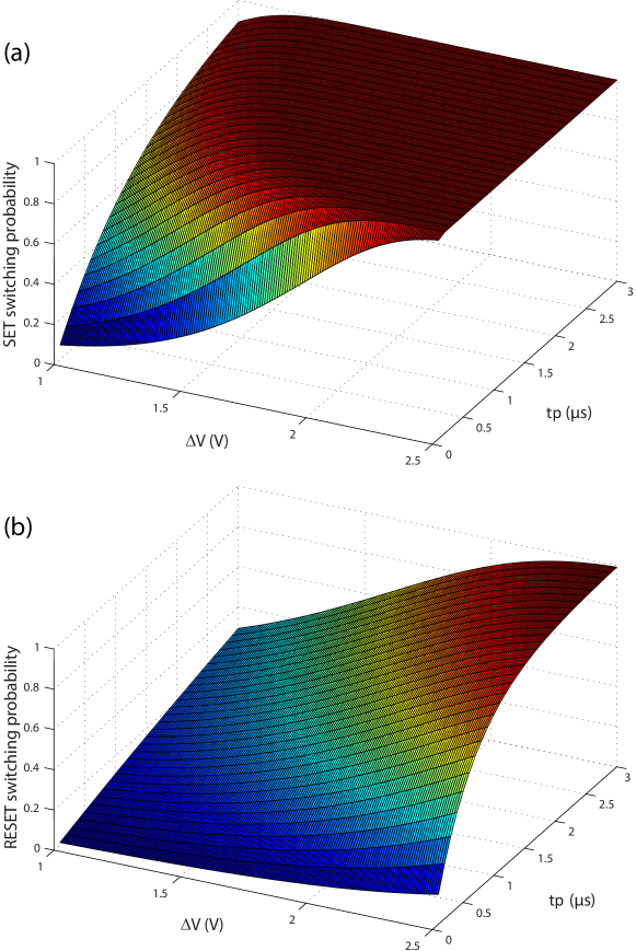
The mentioned experimental studies suggest that the switching probability of redox-based memory is a cumulative phenomenon, which links the digital and analog characteristic of the device. The probabilistic SET and RESET, under such circumstance, can therefore be shown as a function of number of applied pulses with a given amplitude-time combination to model the history dependent effects. One could argue that such spike-history-dependent-plasticity provides further phenomenological similarities between these artificial synapses and the chemical synapses, where history dependent effects also play an important role [19].
This stochastic behavior in combination with results a probabilistic LTP (long-term potentiation) and LTD (long-term depression), which is a function of time difference () between a pre- and a post-synaptic spike (probabilistic spike timing-dependent plasticity, pSTDP) or their difference in voltage (). Stochastic change of the device state can also occur under a sequence of applied pulses with a fixed . The probabilistic plasticity, which defines the probability of change in the device state, is shown in Fig. 3. Here is defined as
| (1) |
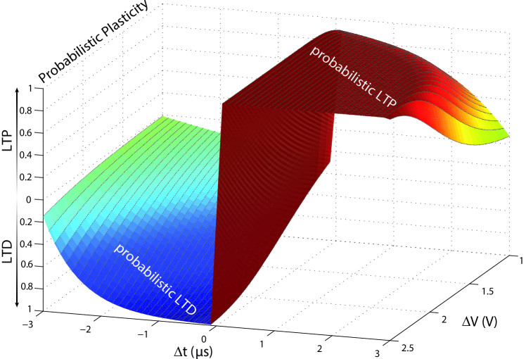
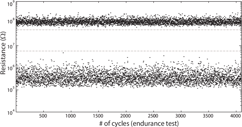
It can be shown that a simple form of , like Eq. (1), is enough to successfully implement a robust and reliable selectivity task. There is a significant cycle-to-cycle resistance variation. This uncertainty is defined and verified using the function . The RRAM and CBRAM devices have experimentally shown log-normal distribution of ON and OFF state resistances. Fig. 4 illustrates high and low resistance variation of a RRAM device for more than switching cycles. In some devices, like [12], OFF state resistances may shows wider variation due to the uncontrolled metallic filament dissolution.
III Orientation Sensitivity
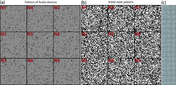
A two layer neural network is implemented with -pixel binary visual images. Inputs were generated using a Gabor-like function to produce more than a thousand, randomly centered, receptive fields. Each input pixel drives an input neuron that spikes if the pixel represents ‘1’. There are nine output neurons that are fully connected to all input neurons through one-bit resolution stochastic RRAM connections. Therefore, synapses are available that are randomly programed and some are faulty. Faulty device patterns, random initial state, and some of the visual inputs are shown in Fig. 5. Output neurons are integration-and-fire neurons that are connected to each other through inhibitory connections, which form a winner-takes-all network. Output neurons could be configured to implement Hebbian, anti-Hebbian, STDP, and anti-STDP learning with a support for a programmable refractory period. The system implements an unsupervised competitive learning that is capable of accepting a wide range of input patterns, including visual and auditory with or without preprocessing.
Energy per spike is an important factor. The model is able to estimate both dynamic switching energy and static leakage power through unselected devices and sneak current paths with or without selector devices. Although, there is little experimental information available regarding spatial variation (device-to-device), the model aims to consider overall impact of such variation with some worst-case assumptions.
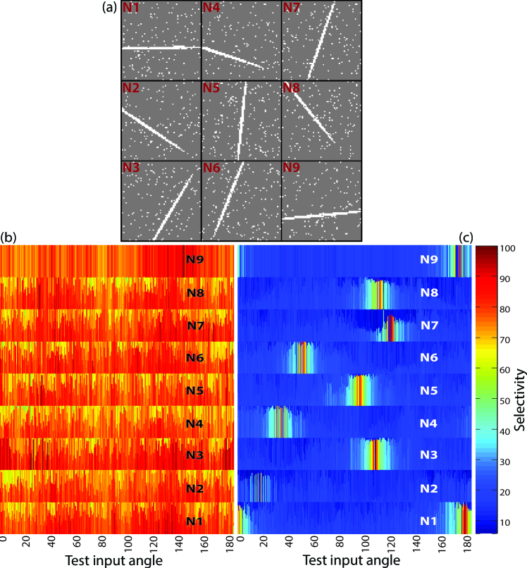
During training, inputs were shown to the network and each was repeated several times. After training, as shown in Fig. 6a, output neurons become sensitive to several orientations. Fig. 6b shows that the system was not sensitive to any angle prior to learning. The system sensitivity to particular angles of the visual input patterns is demonstrated in Fig. 6c. One of the main parameters of designing the system is the dynamic tuning of the output neurons’ firing threshold, which is not the focus of this paper. The training process were repeated with different threshold tuning approaches and a range of initial conditions, device variation, and defect patterns. The system continues to perform reliably under extreme yield (defect rate is ) and variability assumptions, where the function output varies within probability () around its nominal value. Implementing such system with low-power synapses would produce an ultra-high energy efficient and highly scalable system with an energy consumption of pJ/spike.
IV Conclusion
The implemented neuromorphic system is (i) highly scalable, (ii) easily mappable on the current crossbar memory architecture, (iii) not sensitive to device variation, (iv) working reliably with or without selector devices, (v) potentially very high energy efficient, and (vi) potentials for high throughput applications. Each training process, in this case, demands for an endurance requirement in the order of k cycles, which is well within the current reported endurances of RRAM, CBRAM, PCM, STT-MRAM, MeRAM, and atomic switches. Cost-wise, implementing such network with RRAM, CBRAM, PCM, and atomic switches may be cheaper relative to STT-MRAM and MeRAM. However, rapid progress of these technologies promises high energy efficient memory systems, which makes the cost-energy trade-off of these devices more attractive in the near future. Modeling accuracy can be further improved through systematic studies like [13].
Acknowledgements
Omid Kavehei would like to thank Dr Shimeng Yu for his insightful discussions on memory technologies and Ms Nafise Erfanian Saeedi for her comments on the neural network implementation and selectivity.
References
- [1] C. Mead et al., Analog VLSI implementation of neural systems. Springer, 1989.
- [2] E.-A. Vittoz, “Analog VLSI implementation of neural networks,” in IEEE International Symposium on Circuits and Systems, 1990, pp. 2524–2527.
- [3] H. Lim et al., “Short-term memory of TiO2-based electrochemical capacitors: empirical analysis with adoption of a sliding threshold,” Nanotechnology, vol. 24, no. 38, p. 384005, 2013.
- [4] D.-H. O’Connor et al., “Graded bidirectional synaptic plasticity is composed of switch-like unitary events,” Proceedings of the National Academy of Sciences, vol. 102, no. 27, pp. 9679–9684, 2005.
- [5] S. Fusi, “Hebbian spike-driven synaptic plasticity for learning patterns of mean firing rates,” Biological Cybernetics, vol. 87, no. 5-6, pp. 459–470, 2002.
- [6] W. Senn et al., “Convergence of stochastic learning in perceptrons with binary synapses,” Physical Review E, vol. 71, no. 6, p. 061907, 2005.
- [7] J.-S. Seo et al., “A 45nm CMOS neuromorphic chip with a scalable architecture for learning in networks of spiking neurons,” in IEEE Custom Integrated Circuits Conference, 2011, pp. 1–4.
- [8] D. Kuzum et al., “Synaptic electronics: materials, devices and applications,” Nanotechnology, vol. 24, no. 38, pp. 382 001–382 001, 2013.
- [9] M. Suri et al., “Impact of PCM resistance-drift in neuromorphic systems and drift-mitigation strategy,” in IEEE/ACM International Symposium on Nanoscale Architectures, 2013.
- [10] K. Wang et al., “Low-power non-volatile spintronic memory: STT-RAM and beyond,” Journal of Physics D: Applied Physics, vol. 46, no. 7, p. 074003, 2013.
- [11] B. Walmsley et al., “The probabilistic nature of synaptic transmission at a mammalian excitatory central synapse,” Journal of Neuroscience, vol. 7, no. 4, pp. 1037–1046, 1987.
- [12] M. Suri et al., “CBRAM devices as binary synapses for low-power stochastic neuromorphic systems: Auditory (Cochlea) and visual (Retina) cognitive processing applications,” in IEEE International Electron Devices Meeting, 2012, pp. 3–10.
- [13] S. Gaba et al., “Stochastic memristive devices for computing and neuromorphic applications,” Nanoscale, vol. 5, pp. 5872–5878, 2013.
- [14] S. Yu et al., “A low energy oxide-based electronic synaptic device for neuromorphic visual systems with tolerance to device variation,” Advanced Materials, vol. 25, no. 12, pp. 1774–1779, 2013.
- [15] O. Kavehei et al., “Fabrication and modeling of Ag/TiO2/ITO memristor,” in IEEE International Midwest Symposium on Circuits and Systems, 2011, pp. 1–4.
- [16] ——, “An associative capacitive network based on nanoscale complementary resistive switches for memory-intensive computing,” Nanoscale, vol. 5, no. 11, pp. 5119–5128, 2013.
- [17] J.-K. Park et al., “Analysis of resistance variations and variance-aware read circuit for cross-point ReRAM,” in IEEE International Memory Workshop, 2013, pp. 112–115.
- [18] M.-F. Chang et al., “A high-speed -ns read-write random access -Mb embedded resistive RAM (ReRAM) macro using process-variation-tolerant current-mode read schemes,” IEEE Journal of Solid-State Circuits.
- [19] A. Manwani and C. Koch, “Synaptic transmission: An information-theoretic perspective,” Advances in neural information processing systems, pp. 201–207, 1998.