Tunable Superlattice in Graphene To Control the Number of Dirac Points
Abstract
Superlattice in graphene generates extra Dirac points in the band structure and their number depends on the superlattice potential strength. Here, we have created a lateral superlattice in a graphene device with a tunable barrier height using a combination of two gates. In this Letter, we demonstrate the use of lateral superlattice to modify the band structure of graphene leading to the emergence of new Dirac cones. This controlled modification of the band structure persists upto 100 K.
keywords:
Graphene, Superlattice, Dirac points, band structure]Department of Condensed Matter Physics and Materials Science, Tata Institute of Fundamental Research, Homi Bhabha Road, Mumbai 400005, India ]Department of Condensed Matter Physics and Materials Science, Tata Institute of Fundamental Research, Homi Bhabha Road, Mumbai 400005, India ]Department of Condensed Matter Physics and Materials Science, Tata Institute of Fundamental Research, Homi Bhabha Road, Mumbai 400005, India ]Department of Condensed Matter Physics and Materials Science, Tata Institute of Fundamental Research, Homi Bhabha Road, Mumbai 400005, India \altaffiliationBirla Institute of Technology and Science, Pilani, Hyderabad, 500078, India ]Department of Condensed Matter Physics and Materials Science, Tata Institute of Fundamental Research, Homi Bhabha Road, Mumbai 400005, India ]Department of Theoretical Physics, Tata Institute of Fundamental Research, Homi Bhabha Road, Mumbai 400005, India ]Department of Theoretical Physics, Tata Institute of Fundamental Research, Homi Bhabha Road, Mumbai 400005, India ]Theoretical Physics Department, Indian Association for the Cultivation of Science, Kolkata 700032, India ]Department of Condensed Matter Physics and Materials Science, Tata Institute of Fundamental Research, Homi Bhabha Road, Mumbai 400005, India
1
Chirality in graphene provides a unique platform for the experimental observation of phenomena like Klein tunneling1, 2, 3, unusual integer quantum Hall effect4, 5, and rich fractional quantum Hall spectra6, 7. The carrier density in graphene can be changed by applying gate voltages, which allows one to study tunable plasmonic and photonic excitations8, 9, 10, 11, 12, Coulomb drag13 along with technological applications14 like optical modulators15, RF transistors16, and ultrafast and high gain photodetectors17, 18. A technological challenge in working with graphene is the absence of a bandgap. Several methods like chemical functionalization19, nanoribbons20, uniaxial strain engineering21 have been proposed and experimentally demonstrated to modify the band structure of graphene. However, ideas based on chemical functionalization, nanoribbons, and strain engineering do not provide any tunability of properties and their compatibility with large scale integration of devices is yet to be tested. Esaki et al. 22 first proposed the use of a periodic superlattice (SL) potential to modify the band structure in semiconductors and similar experiments have been proposed in monolayer and bilayer graphene23, 24, 25, 26, 27, 28, 29. In contrast to conventional materials, SL in graphene results in anisotropic renormalization of the velocities of the Dirac quasiparticles24, 30 leading to the possibility of collimation31. It also generates extra Dirac points23, 24, 32 in the band structure and these have been experimentally observed in graphene where the substrate induces a periodic potential33, 34, 35, 36. Superlattices using Moire pattern37 by laying graphene over hexagonal boron nitride substrates33 have been demonstrated, but they suffer from the lack of tunability of the superlattice potential. For the first time, here we have created a lateral SL in a graphene device with a tunable barrier height using a combination of two gates with the top-gate consisting of a comb like structure pinned to the same potential. An ability to engineer the band structure of graphene using SL, as we demonstrate, opens up new possibilities.
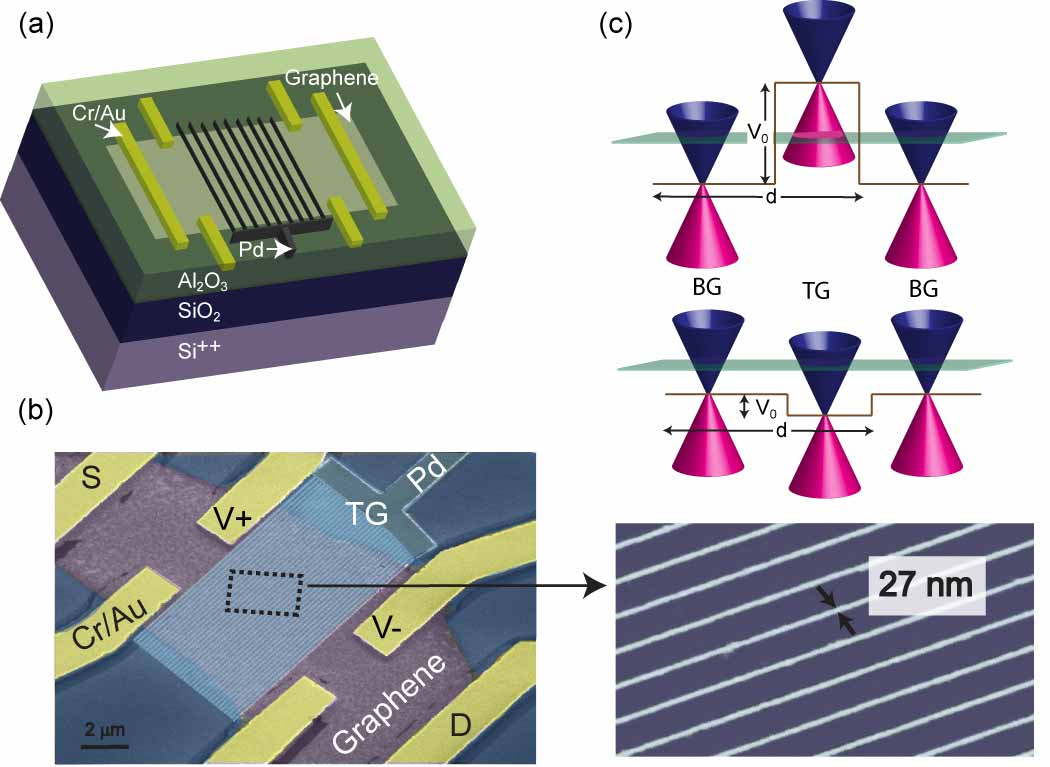
To achieve this goal we fabricate devices in Hall bar geometry with multiple thin top gates defined over the central region of graphene as shown in the schematic in Figure 1a. Figure 1b shows a scanning electron microscope (SEM) image of a device showing multiple (27 nm wide) Pd top gates with a period of 150 nm (details in Section 1 of Supporting Information). The graphene flake can be divided into a series of alternating regions, one with only a back-gate (region denoted as BG) and the other that has both a top-gate (tg) and a back-gate (bg) (region denoted as TG) (see Figure 1c). The charge density in BG region is determined only by the applied back-gate voltage, while in the TG region, it is determined by both the back-gate voltage and the top-gate voltage , providing an independent control to set the charge carrier density and type in the two regions. The amplitude of the SL potential created is the difference in the charge neutral point between the BG and the TG region (illustrated in Figure 1c). The capacitive coupling of the top-gate () is higher than that of the back-gate () due to the geometrical proximity and higher dielectric constant of top-gate dielectric ( 18) (see Section 4 of Supporting Information for details). Fringing fields from the top-gate electrodes lead to the smoothening of the SL potential and the effective width of the top-gate felt by the charge carriers in graphene is approximately 60-70 nm (details regarding the potential profile in Section 9 of the Supporting Information). Varying and , we probe the system having a series of p-n’-p (or n-p’-n) or p-p’-p (or n-n’-n) junctions depending on the combination of the two gate voltages, giving rise to a SL structure in graphene. The advantage of creating a SL structure using gate voltage is that the amplitude of the SL potential can be continuously varied, giving one control over the electronic properties, which is desirable for device applications. In addition, studies have suggested that around 10 periods of the SL are sufficient to see the effect of band formation 38; in our experiments we have used 40 periods of the SL.
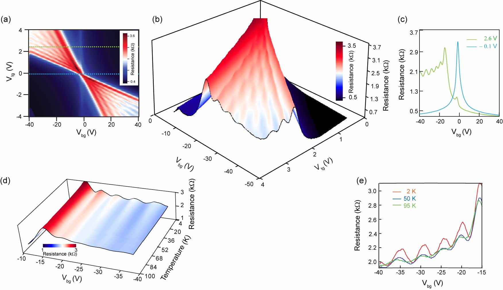
The electrical properties of a monolayer graphene device (evidence for monolayer graphene provided in Section 2 of Supporting Information) are studied using a zero bias measurement. Figure 2a shows the colorscale plot of resistance measured at 300 mK as a function of and . The resistance of the device is low when charge carriers are of the same type in TG and BG region (=1) (top right and bottom left quadrant in Figure 2a). However, when the type of charge carriers in the two regions are different (this happens in part of the bottom right and top left quadrant of Figure 2a), we observe oscillations in resistance as a function of and . These oscillations fade in and out; their number increases with increasing gate voltage as seen in Figure 2b, which is a magnified and detailed measurement of one quadrant of Figure 2a. The number of resistance “ridges” increases by one as the magnitude of and is gradually increased. We note that increasing and in these quadrants amounts to increasing the superlattice barrier seen by the charge carrier and we discuss this aspect later in greater detail. Fixing at 2.6 V, resistance as a function of shows a distinct oscillatory pattern (as shown in green curve in Figure 2c). A slice of the data at the charge neutrality point shows a peak in the resistance at -2 V as seen in the blue curve of Figure 2c. The field effect mobility of this device is 6000 cm2/(Vs) at 300 mK and corresponds to a mean free path of 70 nm (details regarding mobility calculation provided in Section 3 of Supporting Information). The presence of the array of top-gates does not significantly affect the mobility of the device (details in Section 3 of Supporting Information). Another aspect relevant for the transport properties of graphene devices is the depth of the charge puddles 39, 40, 41, 42, Upud, that result from the inhomogeneity of charge distribution. Here, U 71 meV (see Section 3 of Supporting Information) and is comparable with that seen by others in devices with similar mobility.
To further probe the energy and length scale related to the resistance oscillations, we study the transport as a function of temperature. Figure 2d shows the measurement of resistance with gate voltage and temperature (up to 100 K). The oscillations in resistance with gate voltage are robust against temperature and can be seen upto 100 K (8.3 meV), which provides an estimate of the relevant energy scale for the oscillations. The amplitude of the oscillations decrease with increasing temperature, as is clearly seen in the line plots taken at three different temperatures (Figure 2e).(Additional data on temperature variation of oscillations is shown in Section 6 of Supporting Information.)
We would like to note that the resistance oscillations are not as a result of coherent Fabry-Perot resonance of the SL, since the phase coherence 0.6m at 300 mK (details provided in Section 5 of Supporting Information), whereas the SL periodicity is 150 nm. Therefore phase information is lost after 4 SL periods whereas in transport measurement we probe 40 SL periods. The fact that the oscillations persist upto 100 K, where is very small, indicates that the band picture of SL rather than the coherent Fabry-Perot resonances is meaningful in understanding the oscillations in our experiment.
Having considered the experimental results, we now try to understand the potential profile created due to the combination of gates. To the first approximation, we assume that the potential created due to the top-gate is abrupt. The height of the potential created due to the top-gate and back-gate can be calculated from the doping in the two regions, with and without the top-gate; this amounts to measuring the shift in the charge neutrality point in the two regions1. The charge density induced by the back-gate is and that by the top-gate is . The amplitude of the SL potential barrier is then given by (details in Section 8 of Supporting Information)
| (1) |
It is to be noted that for constant amplitude of the potential, in the bottom right quadrant of Figure 2a, we have electrons coming across barriers of constant height, and in the top left quadrant, holes face wells of constant depth. Since the measured data is symmetric, henceforth the magnitude of SL barrier (or well) is referred to as .
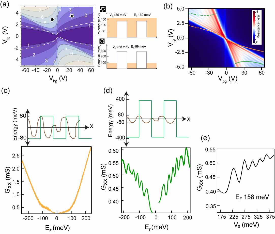
Introduction of the SL potential of period introduces another energy scale which controls the effect of the SL on the system and we examine the experimental results in units of . For our experiments, 150 nm and hence is 4.4 meV. Following eq 1, Figure 3a shows a contour plot of as a function of and for the range of parameters used in our experiments with contours at , where is an integer. To understand the experimental results, we have taken slices of the experimental data along contours of constant . We take slices from the charge neutrality point and note that the charge neutrality point is influenced to some extent by both the gates due to fringing of fields resulting from the structure of the gates. Figure 3b shows the contours along which the slices are taken (dashed for holes corresponding to negative ) (additional slices are shown in Section 8 of Supporting Information).
Figure 3c,d shows slices of the data depicting longitudinal conductance (Gxx) for 6 and 26 respectively. It can be seen from Figure 3c that for 6, we do not observe oscillations in Gxx as is increased. However for higher , oscillations in Gxx become clearly visible as is swept; an example of this is seen in Figure 3d for 26. The reason for this observation is the inhomogeneous charge distribution with U 71 meV (details regarding estimation about electron-hole puddles in graphene in Section 3 of Supporting Information). Because of the presence of puddles, the effects of the periodicity of the SL is not observed unless the depth of the potential modulation is much larger than Upud; this is illustrated by the cartoons in Figure 3c,d. Conductance as a function of at constant also shows oscillatory behavior as seen in Figure 3e.
The relevance of is also observed in the temperature evolution of the resistance oscillations as seen in Figure 2d. For our experiment, 4.4 meV, and we observe that the oscillations in resistance, both as a function of and , become indistinct around 100 K 8.3 meV. The observation that the resistance oscillations are suppressed when temperature exceeds and are seen only when Upud shows that the resistance oscillations arise from the effect of SL potential and this serves as an internal consistency check.
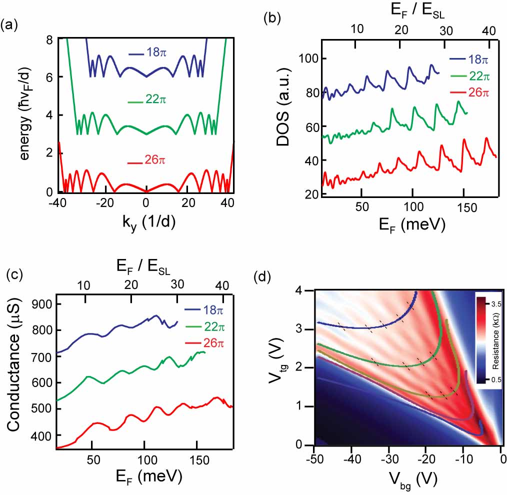
We have already seen indirect experimental evidence (in the form of the energy scale set by the temperature dependence of the oscillations) that the presence of the SL is related to the resistance oscillations. We will now discuss how the SL modifies the graphene band structure, which leads to the experimentally observed resistance oscillations. Several approaches have been followed to study the effects of SL in monolayer and bilayer graphene 23, 24, 25, 26, 38. Here, we will follow the theoretical approach of Barbier et al.24, which obtains the band dispersion of Dirac particles in a square SL potential (with periodic variation along the length of the sample and a constant profile along the width) using a transfer matrix method. We would like to note that, although we use this specific method for ease of application, other approaches also provide very similar predictions 23, 24, 25, 26, 38. The band dispersion of the conduction band of the above mentioned Kronig Penny model for Dirac fermions is plotted as a function of the momentum in the direction, , for 0 in Figure 4a. From top to bottom, the three curves correspond to 18, 22, and 26, respectively. The most dramatic modification of the graphene band structure brought about by the SL is the appearance of additional Dirac points (other than the one at 0), as seen in this figure. The number of additional Dirac points increase by 1 as is increased by 4 (e.g., from 18 which has four additional Dirac points to 22, which has five additional Dirac points).
The relation between appearance of the Dirac points and the resistance oscillations can be understood by looking at the single particle density of states (DOS) calculated from the band dispersion, which is plotted in Figure 4b. The DOS oscillates with the energy (over and above a linearly increasing trend) with peaks corresponding to van Hove singularities occurring between the Dirac points. The number of these peaks follows the number of additional Dirac points in the spectrum and increase with increasing .
The DOS is related to the conductivity through the Einstein relation, , where is the diffusion constant and is the DOS at the Fermi level. In our samples, which have low mobility and hence are in the low diffusive limit where the localization length is much larger than the inter-carrier separation (see Section 10 of Supporting Information for details), the electrical conductivity is dominated by inelastic scattering processes, which allows hopping of the electrons from their localized (but overlapping) wavefunctions. In this case, on dimensional grounds, the diffusion constant , where is a dimensionless constant, is the localization length of the electrons and is the characteristic inelastic scattering time43. In this limit, the conductivity simply mimics the DOS at Fermi level. The resistance oscillations we observe are thus a reflection of the oscillation of the DOS with energy with the number of oscillations tracking the number of additional Dirac points produced in the spectrum by the SL.
In Figure 4c, we plot the experimentally measured conductance as a function of the Fermi energy of the charge carriers. We plot the theoretical data for DOS in Figure 4b and the experimental data for conductance in Figure 4c for the same values of (with the contours of constant shown in the - plane in Figure 4d) and see that they compare well with each other.
Qualitatively, both show a number of oscillations on top of a linearly increasing trend with the number increasing with increasing SL potential. We now proceed to a more quantitative comparison of the theoretical predictions and our experimental data, focusing chiefly on the period of oscillations observed in the two cases. The theoretical DOS oscillates with a period of 21.1 meV, and the experimentally measured conductance oscillates with a period of 27.9 meV. We would like to point out one major factor which can account for this difference, namely, the much smoother profile of the experimental superlattice potential compared to the abrupt square waveform of the Kronig Penny model used in the theory. Brey et al.38 have studied the appearance of extra Dirac point with a smooth potential profile given by and have found that the condition for appearance of new Dirac peaks is given by . The successive Dirac peaks in this case appear when the SL potential is increased by . Thus the period can be significantly affected due to the smoothness of the potential profile. Because of finite thickness of the top gate dielectric, our device lies somewhere in between these two extreme limits. Thus the smoothness of the potential profile qualitatively explains the difference observed between the experimental observations and the theoretical predictions from the simple model. For a more accurate match of theory and experiment, one would have to solve for the dispersion using the actual potential profile of the device, but such calculation would not provide any new insight into the universal property of such devices.
Figure 4d summarizes the main experimental observation showing that as increases by 4, that is, as the number of extra Dirac points increases by one, the number of oscillations increases by one. Another remarkable feature in the data seen in the plot is that in the region of extra Dirac points, the number of oscillations is ; being a positive integer.
In this work we have demonstrated a tunable SL resulting in controllable modification of the band structure. Besides electronic properties, such devices may be of interest for plasmonics and magnetic superlattices could be of interest for spintronic applications. SL structure modifying the band structure also opens ways to realize Weyl semimetal44 predicted in topological insulators and for thermoelectric and spintronic applications45. Our work is a step towards exploring such devices.
We thank Professor Jim Eisenstein for helpful discussions, Dr. Abhilash T.S. for help with the measurement setup and Tanuj Prakash for help with fabrication. We thank Dr. Michael Barbier for sharing the scheme of their calculation. We acknowledge Swarnajayanthi Fellowship of Department of Science and Technology and Department of Atomic Energy of Government of India for support.
References
- Katsnelson et al. 2006 Katsnelson, M. I.; Novoselov, K. S.; Geim, A. K. Nat. Phys. 2006, 2, 620–625
- Shytov et al. 2008 Shytov, A. V.; Rudner, M. S.; Levitov, L. S. Phys. Rev. Lett. 2008, 101, 156804
- Klein 1929 Klein, O. Z. Phys. 1929, 53, 157–165
- Novoselov et al. 2005 Novoselov, K. S.; Geim, A. K.; Morozov, S. V.; Jiang, D.; Katsnelson, M. I.; Grigorieva, I. V.; Dubonos, S. V.; Firsov, A. A. Nature 2005, 438, 197–200
- Zhang et al. 2005 Zhang, Y.; Tan, Y.; Stormer, H. L.; Kim, P. Nature 2005, 438, 201–204
- Bolotin et al. 2009 Bolotin, K. I.; Ghahari, F.; Shulman, M. D.; Stormer, H. L.; Kim, P. Nature 2009, 462, 196–199
- Du et al. 2009 Du, X.; Skachko, I.; Duerr, F.; Luican, A.; Andrei, E. Y. Nature 2009, 462, 192–195
- Chen et al. 2012 Chen, J.; Badioli, M.; Alonso-González, P.; Thongrattanasiri, S.; Huth, F.; Osmond, J.; Spasenović, M.; Centeno, A.; Pesquera, A.; Godignon, P.; Elorza, A. Z.; Camara, N.; Abajo, F. J. G. d.; Hillenbrand, R.; Koppens, F. H. L. Nature 2012, 487, 77–81
- Fei et al. 2012 Fei, Z.; Rodin, A. S.; Andreev, G. O.; Bao, W.; McLeod, A. S.; Wagner, M.; Zhang, L. M.; Zhao, Z.; Thiemens, M.; Dominguez, G.; Fogler, M. M.; Neto, A. H. C.; Lau, C. N.; Keilmann, F.; Basov, D. N. Nature 2012, 487, 82–85
- Yan et al. 2012 Yan, H.; Li, X.; Chandra, B.; Tulevski, G.; Wu, Y.; Freitag, M.; Zhu, W.; Avouris, P.; Xia, F. Nat. Nanotechnol. 2012, 7, 330–334
- Koppens et al. 2011 Koppens, F. H. L.; Chang, D. E.; García de Abajo, F. J. Nano Lett. 2011, 11, 3370–3377
- Lee et al. 2010 Lee, J. M.; Choung, J. W.; Yi, J.; Lee, D. H.; Samal, M.; Yi, D. K.; Lee, C.-H.; Yi, G.-C.; Paik, U.; Rogers, J. A.; Park, W. I. Nano Lett. 2010, 10, 2783–2788
- Gorbachev et al. 2012 Gorbachev, R. V.; Geim, A. K.; Katsnelson, M. I.; Novoselov, K. S.; Tudorovskiy, T.; Grigorieva, I. V.; MacDonald, A. H.; Morozov, S. V.; Watanabe, K.; Taniguchi, T.; Ponomarenko, L. A. Nat. Phys. 2012, 8, 896–901
- Novoselov et al. 2012 Novoselov, K. S.; Fal’ko, V. I.; Colombo, L.; Gellert, P. R.; Schwab, M. G.; Kim, K. Nature 2012, 490, 192–200
- Liu et al. 2011 Liu, M.; Yin, X.; Ulin-Avila, E.; Geng, B.; Zentgraf, T.; Ju, L.; Wang, F.; Zhang, X. Nature 2011, 474, 64–67
- Wu et al. 2011 Wu, Y.; Lin, Y.-m.; Bol, A. A.; Jenkins, K. A.; Xia, F.; Farmer, D. B.; Zhu, Y.; Avouris, P. Nature 2011, 472, 74–78
- Xia et al. 2009 Xia, F.; Mueller, T.; Lin, Y.-m.; Valdes-Garcia, A.; Avouris, P. Nat. Nanotechnol. 2009, 4, 839–843
- Konstantatos et al. 2012 Konstantatos, G.; Badioli, M.; Gaudreau, L.; Osmond, J.; Bernechea, M.; Arquer, F. P. G. d.; Gatti, F.; Koppens, F. H. L. Nat. Nanotechnol. 2012, 7, 363–368
- Elias et al. 2009 Elias, D. C.; Nair, R. R.; Mohiuddin, T. M. G.; Morozov, S. V.; Blake, P.; Halsall, M. P.; Ferrari, A. C.; Boukhvalov, D. W.; Katsnelson, M. I.; Geim, A. K.; Novoselov, K. S. Science 2009, 323, 610–613
- Li et al. 2008 Li, X.; Wang, X.; Zhang, L.; Lee, S.; Dai, H. Science 2008, 319, 1229–1232
- Pereira et al. 2009 Pereira, V. M.; Castro Neto, A. H.; Peres, N. M. R. Phys. Rev. B 2009, 80, 045401
- Tsu and Esaki 1973 Tsu, R.; Esaki, L. Appl. Phys. Lett. 1973, 22, 562–564
- Park et al. 2008 Park, C.-H.; Yang, L.; Son, Y.-W.; Cohen, M. L.; Louie, S. G. Nat. Phys. 2008, 4, 213–217
- Barbier et al. 2010 Barbier, M.; Vasilopoulos, P.; Peeters, F. M. Phys. Rev. B 2010, 81, 075438
- Killi et al. 2011 Killi, M.; Wu, S.; Paramekanti, A. Phys. Rev. Lett. 2011, 107, 086801
- Burset et al. 2011 Burset, P.; Yeyati, A. L.; Brey, L.; Fertig, H. A. Phys. Rev. B 2011, 83, 195434
- Killi et al. 2012 Killi, M.; Wu, S.; Paramekanti, A. Int. J. Mod. Phys. B 2012, 26, 1242007
- Young and Kim 2011 Young, A. F.; Kim, P. Ann. Rev. Condens. Matter Phys. 2011, 2, 101–120
- Tan et al. 2011 Tan, L. Z.; Park, C.-H.; Louie, S. G. Nano Lett. 2011, 11, 2596–2600
- Park et al. 2008 Park, C.-H.; Yang, L.; Son, Y.-W.; Cohen, M. L.; Louie, S. G. Phys. Rev. Lett. 2008, 101, 126804
- Park et al. 2008 Park, C.-H.; Son, Y.-W.; Yang, L.; Cohen, M. L.; Louie, S. G. Nano Lett. 2008, 8, 2920–2924
- Ho et al. 2009 Ho, J. H.; Chiu, Y. H.; Tsai, S. J.; Lin, M. F. Phys. Rev. B 2009, 79, 115427
- Yankowitz et al. 2012 Yankowitz, M.; Xue, J.; Cormode, D.; Sanchez-Yamagishi, J. D.; Watanabe, K.; Taniguchi, T.; Jarillo-Herrero, P.; Jacquod, P.; LeRoy, B. J. Nat. Phys. 2012, 8, 382–386
- Ponomarenko et al. 2012 Ponomarenko, L. A.; Gorbachev, R. V.; Yu, G. L.; Elias, D. C.; Jalil, R.; Patel, A.; Mishchenko, A.; Mayorov, A. S.; Woods, C. R.; Wallbank, J.; Mucha-Kruczynski, M.; Piot, B. A.; Potemski, M.; Grigorieva, I. V.; Novoselov, K. S.; Guinea, F.; Fal´ko, V. I.; Geim, A. K. Nature 2013, 497, 594–597
- Dean et al. 2012 Dean, C. R.; Wang, L.; Maher, P.; Forsythe, C.; Ghahari, F.; Gao, Y.; Katoch, J.; Ishigami, M.; Moon, P.; Koshino, M.; Taniguchi, T.; Watanabe, K.; Shepard, K. L.; Hone, J.; Kim, P. Nature 2013, 497, 598–602
- Pletikosić et al. 2009 Pletikosić, I.; Kralj, M.; Pervan, P.; Brako, R.; Coraux, J.; N’Diaye, A. T.; Busse, C.; Michely, T. Phys. Rev. Lett. 2009, 102, 056808
- Carozo et al. 2011 Carozo, V.; Almeida, C. M.; Ferreira, E. H. M.; Cançado, L. G.; Achete, C. A.; Jorio, A. Nano Lett. 2011, 11, 4527–4534
- Brey and Fertig 2009 Brey, L.; Fertig, H. A. Phys. Rev. Lett. 2009, 103, 046809
- Martin et al. 2008 Martin, J.; Akerman, N.; Ulbricht, G.; Lohmann, T.; Smet, J. H.; Klitzing, K. v.; Yacoby, A. Nat. Phys. 2008, 4, 144–148
- Deshpande et al. 2009 Deshpande, A.; Bao, W.; Miao, F.; Lau, C. N.; LeRoy, B. J. Phys. Rev. B 2009, 79, 205411
- Rossi and Das Sarma 2008 Rossi, E.; Das Sarma, S. Phys. Rev. Lett. 2008, 101, 166803
- Dean et al. 2010 Dean, C. R.; Young, A. F.; Meric, I.; Lee, C.; Wang, L.; Sorgenfrei, S.; Watanabe, K.; Taniguchi, T.; Kim, P.; Shepard, K. L.; Hone, J. Nat. Nanotechnol. 2010, 5, 722–726
- Thouless 1980 Thouless, D. Solid State Commun. 1980, 34, 683–685
- Burkov and Balents 2011 Burkov, A. A.; Balents, L. Phys. Rev. Lett. 2011, 107, 127205
- Song et al. 2010 Song, J.-H.; Jin, H.; Freeman, A. J. Phys. Rev. Lett. 2010, 105, 096403