Electronic properties of site-controlled (111)-oriented zinc-blende InGaAs/GaAs quantum dots calculated using a symmetry adapted Hamiltonian
Abstract
In this work, we present and evaluate a (111)-rotated eight-band Hamiltonian for the zinc-blende crystal lattice to investigate the electronic properties of site-controlled InGaAs/GaAs quantum dots grown along the [111] direction. We derive the rotated Hamiltonian including strain and piezoelectric potentials. In combination with our previously formulated (111)-oriented continuum elasticity model, we employ this approach to investigate the electronic properties of a realistic site-controlled (111)-grown InGaAs quantum dot. We combine these studies with an evaluation of single-band effective mass and eight-band models, to investigate the capabilities of these models for the description of electronic properties of (111)-grown zinc-blende quantum dots. Moreover, the influence of second-order piezoelectric contributions on the polarisation potential in such systems is studied. The description of the electronic structure of nanostructures grown on (111)-oriented surfaces can now be achieved with significantly reduced computational costs in comparison to calculations performed using the conventional (001)-oriented models.
pacs:
68.65.Hb, 71.15.Dx, 73.22.Dj, 78.20.Bh1 Introduction
Quantum dots (QDs) are semiconductor structures which present quantum confinement for charge carriers in all three spatial dimensions on the nanoscale. They range from lithographically patterned systems of electrons [Merkt et al.(1991), Wagner et al.(1992), Pfannkuche et al.(1993), Ezaki et al.(1997), Haryu et al.(1998), Ciftja(2007)] to self-assembled nanocrystals [Hines et al.(1996), Wehrenberg et al.(2002, Kim et al.(2003), Wuister et al.(2004), Brumer et al.(2005), Warner et al.(2005)] and QDs. In particular, QDs from III-V semiconductor materials have attracted considerable research interest during the past years due to their specific electronic and optical properties that make these structures highly promising candidates for a wide variety of novel optoelectronic devices [Michler(2003), Bimberg et al.(2001), Reithmaier and Forchel(2003)]. In particular, the biexciton-exciton cascade in semiconductor QDs has been proposed as a potential candidate for the generation of entangled photon pairs [Benson et al.(2000), Akopian et al.(2006)]. Entangled photon pairs are a key building block for the realisation of novel quantum-logic applications [Knill et al.(2001), Shields(2002)]. In conventional QDs grown on the (001)-surface in zinc-blende (ZB) semiconductors, the generation of entangled photons is difficult due to the -symmetry of the combined system of the underlying crystal lattice and the QD geometry [Bester et al.(2003)]. This symmetry is not high enough to allow for a degeneracy of the bright excitonic ground states [Bester et al.(2003), Seguin et al.(2005)]. The splitting between these states is referred to as the fine-structure splitting (FSS) [Bester et al.(2003), Seguin et al.(2005)]. The problem of a non-vanishing FSS can be overcome by growing site-controlled QDs along the [111] direction in ZB crystals [Pelucchi et al.(2007), Zhu et al.(2007), Juska et al.(2013a)]. In this case the symmetry of the combined system of underlying crystal lattice and QD geometry is [Singh and Bester(2009)], which is high enough to allow in principle for a vanishing FSS [Singh and Bester(2009), Schliwa et al.(2009)]. These theoretical predictions of a minimal FSS in ZB QDs grown along the [111] direction have been confirmed by experiment, i.e. an extremely small FSS has been measured in site-controlled (111)-oriented InGaAs QDs [Dimastrodonato et al.(2010), Mereni et al.(2012), Juska et al.(2013a), Juska et al.(2013b)].
A successful theoretical description of the electronic and optical properties of realistic (111)-oriented site-controlled QDs is highly challenging [Healy et al.(2010)], as these systems can exhibit an extremely small aspect ratio, with base lengths as large as 50-80 nm and heights of only 1-2 nm [Mereni et al.(2009)]. This requires a large supercell and makes atomistic calculations, e.g. employing the empirical tight-binding method (ETBM) [Santoprete et al.(2003), Schulz et al.(2009)] or the empirical pseudopotential method (EPM) [Wang et al.(1999), Bester and Zunger(2005)], computationally highly expensive. Even for continuum-based methods [Bahder(1992), Schliwa et al.(2007), Fonoberov et al.(2007)] the analysis of realistic (111)-oriented InGaAs QDs considered here is computationally very demanding. This originates from the fact that common ZB eight-band models are designed for the description of (001)-oriented systems. A major drawback of this formulation is that the large base length of experimentally observed (111)-grown InGaAs QDs requires a correspondingly large supercell, whereas the small aspect ratio of these dots additionally leads to the need for a highly accurate discretisation in all three spatial dimensions [Healy et al.(2010)]. Therefore, when using a (001)-oriented cell, the QD growth axis is placed along the diagonal of the box and the size of the supercell has to be increased even further to avoid numerical artefacts arising from the boundary conditions. A direct strategy to significantly reduce the computational effort to calculate the electronic properties of (111)-oriented site-controlled InGaAs QDs is to formulate the Hamiltonian in a basis where the [111] direction is chosen as one of the coordinate axes. This formulation directly allows to employ a (111)-oriented supercell and thus enables different mesh discretisations along growth- and in-plane directions. Moreover, and in addition to computational issues, such a formalism is also beneficial to gain deeper insight into the key parameters that determine the electronic and optical properties of (111)-oriented site-controlled InGaAs QDs. As will be shown later, the fundamental weakness of the standard eight-band model, namely the inability to describe the correct symmetry of nanostructures in the zinc-blende crystal [Bester and Zunger(2005)], does not apply to (111)-oriented, -symmetric nanostructures.
For several reasons, as discussed below in detail, Hamiltonians derived in the literature to describe (111)-oriented systems are not directly applicable or have to be validated to be applicable to the here studied QD systems. The effective mass approaches (EMA) presented by Xia et al. [Xia(1991)] and Wei et al. [Wei et al.(2010)] do not take into account band mixing effects, which have been shown to be very important for a realistic description of the electronic structure of conventional, (001)-oriented InGaAs QDs [Wang et al.(2000)]. Four- and six-band Luttinger-Kohn models for (111)-oriented systems, as introduced in Refs. [Ghiti et al.(1990a)], [Seo and Donegan(2003)] and [Kajikawa(1999)], provide a realistic description of the valence band (VB) structure, since they take band mixing effects into account. However, such an approach neglects the coupling between the conduction bands (CB) and the valence bands, which becomes important for semiconductor materials with small energy gaps, such as InAs [Wang et al.(2000)]. Los et al. [Los et al.(1996)] derived general expressions for an eight-band Hamiltonian defined with respect to an arbitrary orientation, taking therefore CB-VB coupling as well as band mixing effects into account. However, an eight-band Hamiltonian for a (111)-oriented system is not explicitly given. Moreover, most of these models are designed to provide an accurate description of quantum wells (QWs) grown on (111)-surfaces [Kajikawa(1999), Mailhiot and Smith(1987), Ikonic et al.(1992), Los et al.(1996)], where the effects of strain are straightforward to include in the Hamiltonian. However, for realistic QD geometries grown on (111)-oriented substrates, position-dependent diagonal and off-diagonal strain tensor components become important in particular when describing the VBs, and therefore need to be included in the model for a consistent description of such dots.
The aim of our present work is to provide a rotated eight-band model using a basis where the [111] direction is chosen as one of the coordinate axes. We also include strain and piezoelectric potentials in a similar manner as in conventional eight-band models [Bahder(1992), Schliwa(2007)], designed for (001)-oriented systems. This approach is then ideally suited to analyse the electronic properties of realistic (111)-grown QDs with large base lengths, both in terms of computing resource demands and also for clarity of interpretation, as we demonstrate through the presentation of calculated electron and hole states in a (111)-oriented InGaAs/GaAs QD structure.
The outline of this paper is as follows. In Sec. 2.1, we derive the rotated eight-band Hamiltonian, taking spin-orbit (SO) coupling, strain, and piezoelectric potentials into account. In Sec. 2.2 we discuss the elastic energy and the (first- and second-order) polarisation vector in a (111)-oriented ZB system. Finally, we apply the (111)-oriented eight-band formalism, including strain and piezoelectric fields to describe the electronic structure of a (111)-grown In0.25Ga0.75As/GaAs QD of realistic dimensions (Sec. 3). Furthermore, we study the validity of a one-band EMA for the conduction and for the valence states. Finally, we summarise our results in Sec. 4.
2 Theory
In this section we describe the theoretical framework employed to analyse the electronic structure of site-controlled (111)-oriented InGaAs/GaAs QDs. Our ansatz can be broken down into two main parts. In the first part, Sec. 2.1, we derive expressions for an eight-band Hamiltonian adapted to a (111)-oriented ZB system. In the second part, Sec. 2.2, we discuss the calculation of the strain and (first- and second-order) piezoelectric potentials in (111)-oriented ZB QDs based on our recent work [Schulz et al.(2011)].
2.1 (111)- Hamiltonian
We derive here an eight-band Hamiltonian to describe the electronic structure of (111)-oriented ZB structures. Our starting point is a conventional eight-band Hamiltonian, designed for a (001)-oriented system, expanded using basis states with symmetry:
The conventional Hamiltonian in this basis is given in A. To obtain a (111)-oriented eight-band Hamiltonian we proceed as described in detail by Voon et al. in Ref. [Lew Yan Voon and Willatzen(2009)]. Following Ref. [Lew Yan Voon and Willatzen(2009)], the rotation of the Hamiltonian from the [001]- to the [111] direction can in general be broken down into three steps. In the first step one neglects the spin and rotates the basis functions of the Hamiltonian. Subsequently, the un-primed wave vector and strain tensor of the (001)-oriented system are replaced by the primed ones and in the (111)-oriented system. In a third step, the matrix is then re-expressed in terms of the modified basis states.
A coordinate rotation matrix going from the (001)- to the (111)-oriented system reads [Schulz et al.(2011)]:
| (1) |
The rotation transforms vectors and tensors from to coordinates via the expressions [Hinckley and Singh(1990)]:
| (2) |
In principle, the spatial transformation given by , has to be combined with a transformation in spin-space. However, it can be shown that the SO coupling matrix elements are independent of the chosen orientation of the basis states with symmetry . This result follows from the fact that the SO interaction is isotropic in a ZB system, which is in contrast to -plane WZ structures where the SO interaction can be different along different directions [Rodina et al.(2001)]. Therefore, in a ZB system, the spatial rotation is already sufficient.
Following this general procedure and taking into account the transformation rules for vectors and tensors, the eight-band Hamiltonian of the (111)-oriented ZB structure, expanded using basis states with symmetry , can be written as:
| (3) |
where and are both matrices. is composed of matrices describing the potential energy part , the kinetic energy part , the SO interaction contribution and a strain dependent part :
| (4) |
The potential energy part of , which contains terms independent of and linear in , is given by:
| (5) |
The CB edge is denoted by while denotes the average unstrained VB edge. and are defined as:
| (6) |
where denotes the SO coupling energy, the fundamental band gap, is the averaged VB edge on an absolute scale and an optional scalar potential describing an electric field, e.g. a piezoelectric built-in field. The Kane parameter is defined as:
| (7) |
where is the mass of an electron and denotes the optical matrix element parameter.
The kinetic energy part in the (111)-oriented systems contains the rotated VB part plus the CB contribution, which is given by . The parameter is defined as:
| (8) |
where denotes the -point CB effective mass. The kinetic energy part of reads:
| (9) |
with
where are the Luttinger parameters for the six-band VB Hamiltonian, defined here in units of . The strain dependent part of the eight-band Hamiltonian , using Einstein summation convention, is given by [222 As discussed by Los et al., [Los et al.(1996)] in the presence of strain, the momentum operator transforms like , where is the unity matrix and the deformation tensor. Therefore, the coupling matrix elements , and with are in principle also modified. This might lead to slightly modified effective masses for the CB and VBs [Aspnes and Cardona(1978)]. However, Los et al. [Los et al.(1996)] argued that strain dependent coupling between CB and VBs is in general small. Therefore, we assume here that the Kane parameter in the (111)-oriented system is the same as in the (001)-oriented system.]:
The matrix elements of the strain dependent part of the Hamiltonian can be obtained from the matrix elements by simply using the substitutions:
| (10) | |||||
| (11) | |||||
| (12) |
The hydrostatic VB deformation potential is denoted by , while and denote the uniaxial deformation potentials.
The SO related contributions and are given by:
| (13) |
and are identical to the contributions in the (001)-oriented system due to the isotropy of the SO interaction in ZB systems.
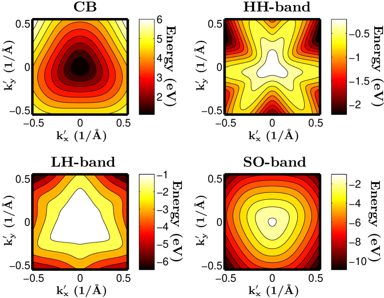
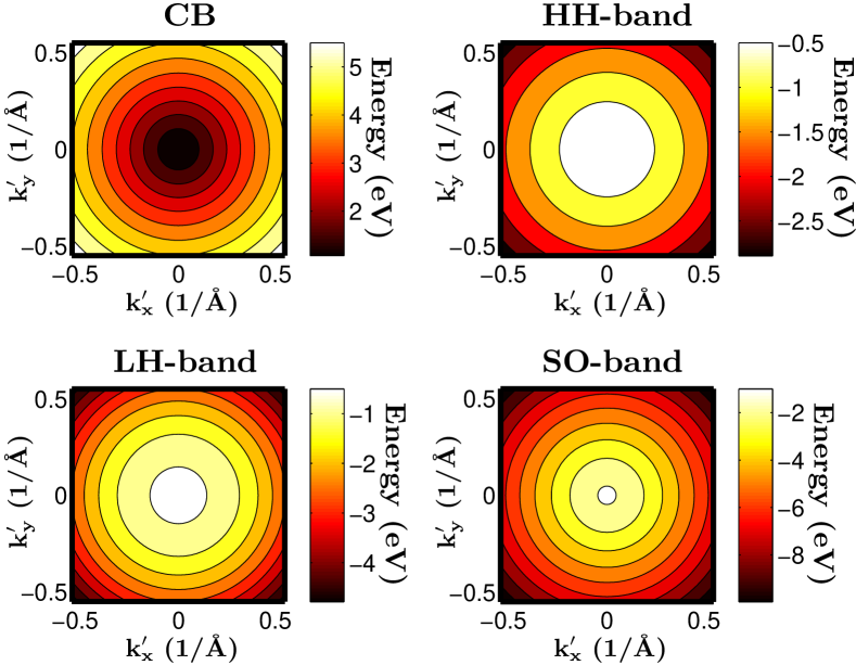
To illustrate the influence of the (111)-growth plane on the conduction- and valence bands, we have calculated the CB and the VBs (HH, LH and SO-band) in the --plane for . The results are shown in figure 1 for InAs in terms of equal energy contours. Here we find that the CB and the VBs clearly exhibit a three-fold symmetry, as expected by considering the point group of a ZB crystal. The tetrahedral point group of a ZB structure contains clockwise and counterclockwise rotations by around the [111]-axis. Therefore, this real space symmetry should also be seen in the band structure. However, the appearance of this three-fold symmetry is also tightly linked to the difference in Kohn-Luttinger parameters and . In the axial approximation, where we set the terms involving () to zero in , the three-fold symmetry vanishes, leading to a CB and VB dispersion which is axially symmetric about the axis. This behaviour is shown in figure 2, where we have artificially switched off terms involving in the Hamiltonian , equation (3).
In order to accurately model the electronic structure of (111)-oriented InGaAs QDs, the three-fold symmetry in CB and VBs needs to be taken into account. It can be seen from figure 1 that the multiband model presented here naturally includes the -symmetry in all directly considered bands.
| GaAs | InAs | |
| (Å) | ||
| (eV) | ||
| (eV) | ||
| (eV) | ||
| (eV) | 28.000 | 22.204 |
| () | 0.067 | 0.022 |
| () | ||
| () | ||
| () | ||
| (eV) | -8.013 | -5.080 |
| (eV) | -8.233 | -6.080 |
| (eV) | ||
| (eV) | ||
| (GPa) | ||
| (GPa) | ||
| (GPa) | ||
| (GPa) | ||
| (GPa) | ||
| (GPa) | ||
| (C/m2) | ||
| (C/m2) | ||
| (C/m2) | ||
| (C/m2) | ||
| (C/m2) | ||
| (C/m2) | ||
| a Ref. [Bhattacharya(1993)] | ||
| b Ref. [Schulz et al.(1982)] | ||
| c Ref. [Adachi(1992)] | ||
| d Ref. [Bester et al.(2006a)] | ||
2.2 Strain and Polarisation in (111)-oriented zinc-blende systems
For a realistic description of the electronic structure of site-controlled InGaAs/GaAs QDs grown on (111)-oriented substrates, knowledge of the strain and the piezoelectric fields is required. In principle, the stress and the electric field are coupled via the Navier equation [Lew Yan Voon and Willatzen(2011)]. However, this coupling has been shown to be very small in InAs/GaAs systems [Lew Yan Voon and Willatzen(2011)]. Therefore, we apply here the widely used ansatz of decoupled electrostatic and elastic equations [Ediger et al.(2007), Schliwa et al.(2007), Fonoberov et al.(2007), Łepkowski(2008), Schliwa et al.(2009), Singh and Bester(2009), Mlinar and Zunger(2009), Zhang et al.(2009), McDonald et al.(2010)], to study the electronic properties of semiconductor nanostructures. In other words, our starting point for the strain field calculation is the elastic energy of the system. Once the strain field is known, it serves as an input for the calculation of the piezoelectric polarisation vector and the resulting piezoelectric built-in potential.
In this section we therefore briefly summarise the results and the expressions we have recently obtained for the elastic energy and the first- and second-order piezoelectric polarisation vectors in (111)-oriented ZB structures. Combined with the rotated eight-band Hamiltonian , introduced in the previous section, this approach offers then an extremely efficient framework to calculate the electronic structure of (111)-oriented ZB nanostructures.
2.2.1 Strain field calculation
Approaches to calculate the strain fields in QD structures range from continuum based to atomistic descriptions. Detailed discussions of the impact of the chosen approach on the resulting strain field have been given in a number of publications [Pryor et al.(1998), Stier et al.(1999)]. The choice of the strain model also depends on the choice of the model for the electronic structure calculation. Schliwa et al. discussed in detail that a continuum elasticity model is the optimal choice for an eight-band approach [Schliwa et al.(2007)]. Furthermore, our previous analysis showed [Schulz et al.(2011)] that the use of a continuum based ansatz to calculate the strain field in QD structures grown on a (111)-oriented ZB substrate is already able to capture the correct symmetry of the system [Singh and Bester(2009)].
As described above, our starting point for the continuum based description of the strain field in a nanostructure is the total elastic energy of the system. To obtain the strain field in a given nanostructure, the elastic energy of the system under consideration is minimised with respect to the displacements . Once the displacements are known throughout the simulation cell, the strain field can be obtained. More details on strain field calculations in (111)-oriented ZB systems are given in Ref. [Schulz et al.(2011)]. In a second-order continuum elasticity formulation the elastic energy in a uniformly strained (111)-oriented ZB system of volume is given by [Schulz et al.(2011)]:
| (14) | |||||
where denotes the different components of the strain tensor in the (111)-oriented system while are the components of the stiffness tensor. The components have been calculated from the elastic constants of the (001)-system according to the equations given in Ref. [Schulz et al.(2011)] and are summarised in table 1.
The expression for the elastic energy of a (111)-oriented ZB structure is very similar to that for the elastic energy of a -plane WZ system [Schulz et al.(2011)]. The major difference in the above expression compared to that for the elastic energy of a WZ system arises from the terms related to . However, it should be noted that is at least a factor of 2.5 smaller than the remaining elastic constants . Therefore, slight modifications in the strain field of a (111)-oriented ZB QD compared to a WZ-like system are introduced by the related terms. A detailed discussion of strain fields in (111)-oriented ZB structures in comparison to a WZ-like system is also given in Ref. [Schulz et al.(2011)].
2.2.2 First- and second-order piezoelectric polarisation
Semiconductor materials with a lack of inversion symmetry exhibit under applied stress an electric polarisation [Cady(1946)]. This strain dependent polarisation is referred to as the piezoelectric polarisation.
In the linear regime, the piezoelectric polarisation vector is connected to the strain state of the system via the piezoelectric coefficient . However, non-linear contributions to the piezoelectric polarisation fields have been observed in experimental studies on (111)-oriented InGaAs QWs [Dickey et al.(1998), Cho et al.(2001), Sánchez et al.(2002)]. To take these non-linear effects in the piezoelectric polarisation into account, different approaches have been proposed in the literature [Bester et al.(2006a), Migliorato et al.(2006)]. A detailed overview of these different schemes is given in the recent review article by Lew Yan Voon and Willatzen [Lew Yan Voon and Willatzen(2011)]. A widely used approach [Bester et al.(2006b), Ediger et al.(2007), Schliwa et al.(2007), Łepkowski(2008), Schliwa et al.(2009), Singh and Bester(2009), Mlinar and Zunger(2009), Zhang et al.(2009), McDonald et al.(2010)], even though it is surrounded by some controversy [Migliorato et al.(2006), Lew Yan Voon and Willatzen(2011)], was developed by Bester et al. [Bester et al.(2006a)]. The authors have introduced a second-order piezoelectric tensor and calculated its coefficients. Due to the symmetry of the system, one is left with only three non-vanishing coefficients , and . The values of these coefficients have recently been presented for the most common III-V ZB alloys [Beya-Wakata et al.(2011)], including some changes and updating of the previously reported values [Bester et al.(2006a)]. We will therefore provide a more detailed discussion of the influence of different first- and second-order piezoelectric constants on the polarisation potential of (111)-oriented InGaAs QDs in Sec. 3.2.
In order to achieve a higher efficiency of the calculations and a deeper insight into the key parameters that determine the polarisation characteristics of (111)-oriented ZB QDs, we have derived expressions for the first- () and second-order () polarisation vectors in a basis where the [111] direction is chosen as one of the coordinate axes. This basis is identical to the basis we have used here, to obtain the eight-band Hamiltonian , equation (3), of a (111)-oriented system. The first-order piezoelectric polarisation vector is given by [Schulz et al.(2011)]:
| (15) |
The strain tensor components in the (111)-ZB system are denoted by . We introduce the coefficients following our previous work [Schulz et al.(2011)] to simplify the expressions for the second-order components.
In the (111)-oriented ZB system, the second-order piezoelectric polarisation vector reads [Schulz et al.(2011)]:
| (16) |
with
and
The coefficients and are related to the piezoelectric coefficients and by
| (17) |
with the coefficients and describing the second order piezoelectric response associated respectively with hydrostatic and biaxial strain. We note that the components of the second-order piezoelectric vector (hydrostatic strain term) in equation (16) are directly proportional to those for the first order term in equation (15).
Once and are known for a given structure, the corresponding piezoelectric potentials can be calculated by solving the Maxwell equation . More details are given in Ref. [Schulz et al.(2011)].
3 Results
In this section we present our results on the electronic structure of site-controlled (111)-oriented InGaAs QDs. In a first step we review experimental data on the structural properties of these systems. We briefly discuss the strain and electrostatic built-in fields in these systems and point out some similarities and differences to conventional (001)-oriented InGaAs QDs. A more detailed discussion is given in Ref. [Schulz et al.(2011)]. Finally, in Sec. 3.3, we focus on the single-particle electron and hole states in a realistic site-controlled (111)-oriented InGaAs QD.
3.1 Model geometry
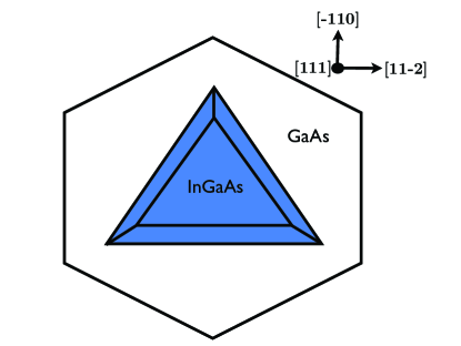
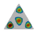
Experimental data on site-controlled (111)-oriented InGaAs QDs indicate a triangular-shaped QD geometry [Pelucchi et al.(2004)]. As discussed above, these triangular-shaped QDs exhibit a very small aspect ratio with base lengths of order 50-80 nm and heights of only 1-2 nm [Healy et al.(2010)]. The reported indium concentration in the site-controlled (111)-oriented InGaAs QDs considered here ranges from 15% to 45% [Healy et al.(2010)]. Therefore, in accordance with these experimental findings, we choose a triangular In0.25Ga0.75As QD grown on the (111)-surface with a triangle side length of 80 nm and a height of 2 nm. The QD is embedded in a GaAs matrix. A schematic illustration of such a QD is shown in Fig. 3.
Making use of the advantages of the (111)-rotated model introduced above, we have discretised our simulation cell in steps of 4 nm in-plane and 0.5 nm along the growth direction (the [111] direction), to achieve a reasonable computational effort for our calculations. Due to the plane-wave framework of the S/Phi/nX [Marquardt et al.(2010), Boeck et al.(2011)] software package used for our calculations, periodic boundary conditions are assumed. All material parameters employed in our calculations are listed in table 1. To increase the efficiency of these calculations in a (111)-oriented cell, we have moreover made use of a hexagonal shaped supercell, where the symmetry of the simulation cell does not interfere with the symmetry of the combined system of the underlying lattice and QD geometry. Of course the question of the electronic structure of site-controlled (111)-oriented InGaAs QD can, in principle, also be addressed by means of EPM or ETBM approaches. However, as in the case of conventional -Hamiltonians, simulation packages such as Nemo3D [Klimeck et al.(2002)] (ETBM) are primarily designed for (001)-oriented ZB structures. Therefore, the underlying atomic grid has to be adjusted for the system under consideration. Furthermore, as the experimentally observed QDs exhibit large base lengths of up to 80 nm, and because the dots are considered as isolated systems, it is required to provide a sufficiently large unit cell around the QD, in order to avoid artefacts arising from the long-range piezoelectric potential or strain. Thus, supercells employed can easily exceed dimensions of 200 nm along the in-plane directions and 50 nm along the [111] growth direction, since hexagonal or triangular-shaped cells are not the standard implementation in most simulation packages. Therefore, supercells dimensions of at least are required for the QDs considered here, which corresponds to almost 90 million atoms, making more sophisticated atomistic calculations extremely cumbersome and time-consuming, with considerable requirements for computational resources. The benefit of the here presented -Hamiltonian for (111)-oriented ZB systems in conjunction with the S/Phi/nX software library is that a ready-to-use solution to the problem of the electronic structure of (111)-oriented InGaAs QDs is provided. The module of the S/Phi/nX package has been developed to accept any arbitrary -band Hamiltonian as an input file, where the Hamiltonian is set up in an input file in a human readable meta-language [Marquardt et al.(2011)]. Therefore, no additional coding is required once the desired Hamiltonian has been prepared.
3.2 Strain and polarisation potential
As known from (001)-oriented InGaAs QDs, strain and built-in fields significantly modify the electronic and optical properties of epitaxially grown QD systems. Recently, we have discussed in detail the strain and built-in fields in (111)-oriented InGaAs QDs [Schulz et al.(2011)]. Our results have shown that the strain, first- and second-order built-in fields exhibit a three-fold symmetry () even if the QD geometry possesses a higher symmetry, e.g. symmetry. This symmetry is further emphasised by the triangular shape of realistic site-controlled (111)-oriented InGaAs QDs. Moreover, and in contrast to (001)-oriented InGaAs QDs, one finds a potential drop along the growth direction of the nanostructure. This behaviour is similar to a nitride-based WZ structure [Williams et al.(2009)]. However, the potential drop in a realistic nitride WZ nanostructure is much larger due to the much larger piezoelectric coefficients and the spontaneous polarisation which is missing in ZB systems [Schulz et al.(2011)]. This potential drop also affects the single-particle states of (111)-oriented InGaAs QDs. Depending on the dot height and In concentration, this effect might lead to a spatial separation of electron and hole wave functions, diminishing therefore the oscillator strength of interband transitions. Furthermore, as shown by Schliwa et al. [Schliwa et al.(2007)] for (001)- and (111)-oriented InGaAs QDs, the balance between first- and second-order piezoelectric contributions is very sensitive to the QD shape, size and composition. Therefore, the detailed theoretical analysis of the electronic and optical properties of high-quality site-controlled (111)-oriented InGaAs QDs in combination with experimental studies provides a very promising route to gain deeper insight into non-linear piezoelectric effects in ZB semiconductor materials.
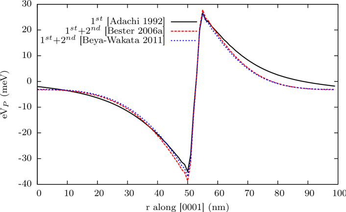
Following our discussion in Sec. 2.2, we have calculated the polarisation potential in our model QD using only first-order and first- plus second-order contributions to evaluate the influence of second-order piezoelectric effects on the polarisation potential of the system. Modified values have recently been presented [Beya-Wakata et al.(2011)] for the first- and second-order piezoelectric constants for InAs and GaAs originally reported in Ref. [Bester et al.(2006a)]. In particular, the parameter differs from the previously reported value. This parameter changes its sign for InAs, compared to the previous value. The sign remains the same in GaAs, but the absolute value differs from the previous parameter set by about . However, as we have demonstrated recently, for the total built-in potential in (111)-oriented InAs/GaAs QDs, contributions arising from terms are of secondary importance [Schulz et al.(2011)]. Moreover, the changes in the dominant parameters and , equation (17), are % [cf. table 2]. Therefore, only slight changes in the total built-in potential are expected in (111)-oriented InGaAs/GaAs QDs when using the two different parameter sets. However, for the sake of completeness, our calculations employing both first- and second-order contributions were carried out with the two different parameter sets. In doing so, we were able to identify the quantitative influence of the different parameter sets on the polarisation potential. Overall, we find second-order piezoelectric effects to have a non-negligible influence on the polarisation potentials. However, as expected from the discussion above, only minor modifications on the polarisation potential arise from the choice of different parameter sets for the second-order piezoelectric contributions. In particular, we have not seen any qualitative change of the polarisation potential in our QD system and quantitative changes are small as the minima and maxima of the resulting polarisation potential, shown in table 2, indicate. Based on this evaluation, we have performed our calculations using the first- and second-order piezoelectric constants from Ref. [Bester et al.(2006a)].
| Ref. [Adachi(1992)] | Ref. [Bester et al.(2006a)] | Ref. [Beya-Wakata et al.(2011)] | ||||
| Parameter | InAs | GaAs | InAs | GaAs | InAs | GaAs |
| [] | -0.045 | -0.160 | -0.115 | -0.230 | -0.115 | -0.238 |
| [] | n.a. | -0.531 | -0.439 | -0.6 | -0.4 | |
| [] | n.a. | -4.076 | -3.765 | -4.1 | -3.8 | |
| [] | n.a. | -0.120 | -0.492 | 0.2 | -0.7 | |
| [] | n.a. | -2.894 | -2.656 | -2.933 | -2.667 | |
| [] | n.a. | 2.363 | 2.217 | 2.333 | 2.267 | |
| min() [mV] | -35.9 | -38.1 | -39.8 | |||
| max() [mV] | 28.3 | 30.4 | 31.8 | |||
 |
 |
 |
 |
| = 1491.4 meV | = 1497.4 meV | = 1497.4 meV | = 1503.6 meV |
| : 0.0012 | : 0.0027 | : 0.0026 | : 0.0039 |
| : 0.0012 | : 0.0026 | : 0.0027 | : 0.0040 |
| : 0.0107 | : 0.0110 | : 0.0109 | : 0.0105 |
| : 0.9870 | : 0.9830 | : 0.9840 | : 0.9818 |
 |
 |
 |
 |
| = 64.9 meV | = 63.5 meV | = 63.4 meV | = 61.2 meV |
| : 0.4989 | : 0.4969 | : 0.4950 | : 0.4933 |
| : 0.4976 | : 0.4940 | : 0.4970 | : 0.4927 |
| : 0.0035 | : 0.0081 | : 0.0069 | : 0.0121 |
| : 0.0001 | : 0.0011 | : 0.0011 | : 0.0018 |
3.3 Single-particle states
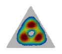
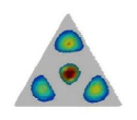
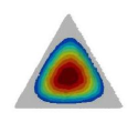
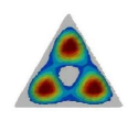
The formalism derived in Sec. 2.1 has been employed and evaluated for the description of the electronic properties of a (111)-oriented, site-controlled In0.25Ga0.75As/GaAs QD of triangle side length 80 nm and of height 2 nm. Figure 4 shows the eigenenergies, charge densities and orbital contributions of the first four localised electron and hole states. Please note, each state is twofold Kramer’s degenerate. The electron states are dominated by the and states with only small contributions from the , , and bands. All four hole states depicted in Fig. 4 are predominantly HHs with large , , and contributions to the eigenstates, and only a small contribution from , , and components.
Additionally, a spatial separation of electron and hole charge densities is observed, resulting from the polarisation potential shown in figure 5, where a potential drop is visible, similar to those in WZ QDs along the growth direction. As a result of the flat shape of the QD with a height of only 2 nm and the correspondingly weak charge carrier localisation, the electron ground state binding energy is quite close to the GaAs CB, resulting in a calculated ground state single-particle transmission energy of approx. 1428.3 meV. This value is smaller than the one reported by Juska et al. [Juska et al.(2011)] of 1462.5 meV. However, our model QD has a larger thickness than the one reported in this reference, which leads to lower quantisation energies in our system. Previous measurements on site-controlled InGaAs/GaAs QDs reported smaller emission energies of around 1304 meV [Gallo et al.(2008)], resulting from different dimensions (base lengths of 20 nm and heights of 5 nm), and material composition. When looking at the charge densities in more detail (Figure 4), one finds that the electron and hole ground state wave functions can be classified according to their nodal structure as being -like. The following excited electron states exhibit p-like nodal structures. First and second excited states are moreover degenerate as a consequence of the system’s symmetry. However, the classification of the first three excited hole states is more complicated due to the underlying symmetry of the system. The first two excited hole states, and , neglecting the Kramer’s degeneracy of these states, are almost degenerate. From the symmetry of the system one might have expected an exact degeneracy. Since our calculations take SO coupling effects into account, one has to deal with the double group which allows for twofold degenerate states only [Schulz et al.(2008)]. If we artificially switch off the SO coupling in our calculations and neglect strain and polarisation potentials, the states and are indeed degenerate. Strain and polarisation potentials calculated from a continuum-elasticity model as described in Ref. [Schulz et al.(2011)] do not reduce the symmetry of our model QD and thus do not induce a splitting of degenerate states.
The computational effort of simulating electronic properties in a (111)-oriented QD with such an extremely small aspect ratio can be further reduced strongly by employing a one-band EMA instead of a multiband approach. Moreover, the large base length and the small height of the QD suggest an almost QW-like behaviour, such that an EMA might in fact be suited to provide an accurate description of the confined states in such a system. To evaluate the applicability of simplified EMA models, we compare now the results of the single-band effective mass model with those from an eight-band approach used to describe the electronic properties of our model system. In the single-band effective mass case, we consider an isotropic electron mass :
| (18) |
The hole effective mass is different along the [111]-growth direction and in the in-plane directions and :
| (19) | |||||
Table 3 summarises the electron and hole eigenenergies obtained from the two models with respect to the bulk GaAs VB edge.
| model | ||||||||
|---|---|---|---|---|---|---|---|---|
| 8-band | 1491.4 | 1497.4 | 1497.4 | 1503.6 | 64.9 | 63.5 | 63.4 | 61.2 |
| EMA | 1492.4 | 1498.7 | 1498.7 | 1505.0 | 63.6 | 60.6 | 60.6 | 56.4 |
It can be seen that the EMA-based results are in broad agreement with but show some deviations from the eight-band model. In addition, the EMA neglects the SO coupling, such that the first and second excited hole state are expected and found to be energetically degenerate, which can represent a significant difference to results obtained from an eight-band model, depending on QD geometry and composition.
While the charge densities of the states under consideration do not differ significantly between the EMA and the full eight-band model, the electron and hole eigenenergies are modified in the order of 1 to 5 meV between the two models (cf. table 3). The EMA is therefore able to provide a good qualitative description of the charge densities of electrons and holes. The eigenvalues do similarly agree well between EMA and eight band models. Since the first four hole states are almost exclusively and -like with negligible -like components ( indicates spin-up and spin-down, respectively), the here calculated bound hole states are predominantely of HH character. This is in contrast to previous findings [Karlsson et al.(2010)], where the hole ground state is 89% HH-like while the first excited state is a LH-like state (91%). We attribute this difference to the difference in the QD dimensions; the very small aspect ratio here leads to the increased HH character for the highest valence states.
Once the electronic structure of the site-controlled (111)-oriented QDs is known, one can start to analyse the optical properties of these systems. This task is beyond the scope of the present study. However, from the electronic structure results derived here, one can already start to discuss the procedure necessary to accurately describe the optical properties, such as the FSS, of the system under consideration. For an accurate description of the FSS, configuration interaction (CI) calculations are often applied [Bester et al.(2003), Seguin et al.(2005), Baer et al.(2005), Schliwa(2007)]. Such an approach takes not only the direct Coulomb interaction between the carriers into account, it accounts also for exchange and correlation contributions. In the CI scheme, the many-body Hamiltonian is expanded in the basis of anti-symmetrised products of bound single-particle electron and hole states. In the case of (001)-oriented InGaAs QDs, the CI scheme has been successfully applied to study the FSS in these systems [Seguin et al.(2005), Bester et al.(2003)]. However, the accuracy of this approach depends strongly on the number of bound states taken into account in the expansion [Wimmer et al.(2006)]. For example, Bester et al. [Bester et al.(2003)] included 12 electron and 12 hole single-particle states in the CI expansion to obtain reliable results for the FSS in (001)-oriented InGaAs QDs. Our calculations indicate all electronic states are close to the GaAs band edges, such that only a small number of localised charge carriers can be expected. It may thus become important to employ other techniques that do not rely on a larger number of localised electronic states.
One strategy to circumvent the problems arising from a small number of bound electron and hole states is to perform first a self-consistent Hartree-Fock calculation and use the results from this calculation as an input for the CI approach [Kindel et al.(2010)]. Such calculations could address issues such as the difference in binding energy of excitons and biexcitons. However, it should be noted that disorder effects can break the symmetry in a (111)-oriented QD and are therefore critical to determining the value of the FSS. We note that there will be alloy-related disorder in the InGaAs QD layer. As the energy differences between the hole states in the dot considered here are only of the order of a few meV, it can be expected that disorder effects may lead to a mixing of the different hole states presented in figure 4, even in a single-particle picture [Watson-Paris et al.(2011)]. These disorder effects will therefore need to be included in more detailed calculations of the dependence of FSS on dot size, shape and composition. Thus, in addition to the very challenging task to calculate the electronic structure of realistic (111)-oriented, site-controlled InGaAs QDs, the accurate description of the optical properties will be even more challenging, due to the self-consistent cycles and disorder effects. The symmetry adapted formalism presented here then provides one of the key building blocks to address this problem.
4 Conclusion
We have presented a (111)-rotated eight-band model for the description of ZB QDs grown on a (111)-oriented surface. We have applied our model to the case of a site-controlled In0.25Ga0.75As/GaAs QD with its experimentally observed small aspect ratio to calculate electron and hole single-particle states in these systems. Our approach yields a significant reduction of the computational effort, by using a Hamiltonian that is adapted to the specific properties of (111)-oriented supercells. A detailed study showing the influence of strain and polarisation potentials on the electronic properties has been performed. A recently published set of first- and second-order piezoelectric constants does not significantly alter the outcome of our calculations in comparison to the previous parameter set. A comparison to the effective mass simplification revealed the qualitative ability of less sophisticated models to provide a good description of electron and hole charge densities, while some modifications in the eigenenergies occur for the case of the EMA, outlining the importance of such an eight-band model. Our results highlight the need for a symmetry adapted approach as a first step to calculate the electronic structure of such systems. We conclude that our rotated eight-band model is well suited to a description of realistic, (111)-oriented ZB QDs and can be used in combination with our previous work on the correspondingly rotated continuum elasticity model, to carry out broad studies on various possible modifications of realistic site-controlled, (111)-oriented InGaAs/GaAs QDs, as well as on other materials that exhibit a ZB crystal lattice. Our work in combination with the module of the S/Phi/nX software library provides a ready-to-use approach to the electronic properties of (111)-oriented ZB QDs, allowing in general for a reliable and computationally inexpensive simulation of these novel nanostructures.
Appendix A Eight-band Hamiltonian in the (001)-system
The eight-band Hamiltonian in a (001)-ZB structure, expanded into basis states with symmetry can be written in the following block matrix form [Schliwa(2007)]:
| (20) |
where and are 4 matrices. The complex conjugate is denoted by ∗. can be divided into four sub-matrices (potential energy part; terms independent of and linear in ), (kinetic energy part; terms quadratic in ), (strain dependent part) and (SO part): . The matrix , describing terms independent of and linear in , is given by:
| (21) |
The matrix includes the CB edge energy and the average VB edge energy , described by the matrix . and are defined in equation (6). The Kane coupling parameter is defined in equation (7).
The kinetic energy part of for the eight-band Hamiltonian is given by :
The parameter is defined in equation (8). Following Schliwa et al. [Schliwa et al.(2007)], we neglect the quadratic coupling between the CB and VBs which is related to the Kane parameter .
The VB part is described by the matrix :
with , and given by
where is the fundamental band gap of the material under consideration and are the Luttinger parameters, given in units of , with being the mass of the electron.
The strain dependent part is given by:
with , and , and where denotes the different strain tensor components. The hydrostatic deformation potential of the VB is denoted by while denotes the hydrostatic deformation potential of the CB. The uniaxial VB deformation potentials are given by and . Following Schliwa et al. [Schliwa et al.(2007)], we neglect shear-strain related CB-VB coupling. The SO coupling is described by the matrices and , which are identical to , and , given in equation (13).
References
- [Merkt et al.(1991)] U. Merkt, J. Huser, and M. Wagner, Phys. Rev. B 43, 7320 (1991).
- [Wagner et al.(1992)] M. Wagner, U. Merkt, and A.V. Chaplik, Phys. Rev. B 45, R1951 (1992).
- [Pfannkuche et al.(1993)] D. Pfannkuche, V. Gudmundsson, and P.A. Maksym, Phys. Rev. B 47, 2244 (1993).
- [Ezaki et al.(1997)] T. Ezaki, N. Mori, and C. Hamaguchi, Phys. Rev. B 56, 6428 (1997).
- [Haryu et al.(1998)] A. Haryu, V.A. Sverdlov, B. Barbiellini, and R.M. Nieminen, Physica B: Condens. Matter 255, 145 (1998).
- [Ciftja(2007)] O. Ciftja, J. Phys.: Condens. Matter 19, 046220 (2007).
- [Hines et al.(1996)] M.A. Hines, and P. Guyot-Sionnest, J. Phys. Chem. 100, 468 (1996).
- [Wehrenberg et al.(2002] B.L. Wehrenberg, C. Wang, and P. Guyot-Sionnest, J. Phys. Chem. B 106, 10634 (2002).
- [Kim et al.(2003)] S. Kim, and M.G. Bawendi, J. Am. Chem. Soc. 125, 14652 (2003).
- [Wuister et al.(2004)] S.F. Wuister, C.d.M. Donegá, and A. Meijerink, J. Chem. Phys. 121, 4310 (2004).
- [Brumer et al.(2005)] M. Brumer, A. Kigel, L. Amirav, A. Sashchiuk, O. Solomesch, N. Tessler, and E. Lifshitz, Adv. Funct. Mater. 15, 1111 (2005).
- [Warner et al.(2005)] J.H. Warner, E. Thomsen, A.R. Watt, N.R. Heckenberg, and H. Rubinsztein-Dunlop, Nanotechnology 16, 175 (2005).
- [Michler(2003)] P. Michler, Single Quantum Dots: Fundamentals, Applications, and New Concepts, vol. 90 of Topics in Applied Physics (Springer, Berlin, 2003).
- [Bimberg et al.(2001)] D. Bimberg, M. Grundmann, and N. N. Ledentsov, Quantum Dot Heterostructures (Wiley, Chichester, 2001).
- [Reithmaier and Forchel(2003)] J. P. Reithmaier and A. Forchel, IEEE Circuits and Devices Magazine 19, 24 (2003).
- [Benson et al.(2000)] O. Benson, C. Santori, M. Pelton, and Y. Yamamoto, Phys. Rev. Lett. 84, 2513 (2000).
- [Akopian et al.(2006)] N. Akopian, N. H. Lindner, E. Poem, Y. Berlatzky, J. Avron, D. Gershoni, B. D. Gerardot, and P. M. Petroff, Phys. Rev. Lett. 96, 130501 (2006).
- [Knill et al.(2001)] E. Knill, R. Laflamme, and G. J. Milburn, Nature (London) 409, 46 (2001).
- [Shields(2002)] A. Shields, Science 297, 1821 (2002).
- [Bester et al.(2003)] G. Bester, S. Nair, and A. Zunger, Phys. Rev. B 67, 161306(R) (2003).
- [Seguin et al.(2005)] R. Seguin, A. Schliwa, S. Rodt, K. Pötschke, U. W. Pohl, and D. Bimberg, Phys. Rev. Lett. 95, 257402 (2005).
- [Pelucchi et al.(2007)] E. Pelucchi, S. Watanabe, K. Leifer, Q. Zhu, B. Dwir, P. De Los Rios, and E. Kapon, Nano Lett. 7, 1282 (2007).
- [Zhu et al.(2007)] Q. Zhu, K. F. Karlsson, E. Pelucchi, and E. Kapon, Nano Lett. 7, 2227 (2007).
- [Juska et al.(2011)] G. Juska, V. Dimastrodonato, L. O. Mereni, A. Gocalinska, and E. Pelucchi, Nat. Photonics 7, 527 (2013).
- [Juska et al.(2013a)] G. Juska, V. Dimastrodonato, L. O. Mereni, A. Gocalinska, and E. Pelucchi, Nanoscale Research Letters 6, 567 (2013).
- [Juska et al.(2013b)] G. Juska, V. Dimastrodonato, L. O. Mereni, A. Gocalinska, and E. Pelucchi, Nature Photonics 7, 527 (2013).
- [Singh and Bester(2009)] R. Singh and G. Bester, Phys. Rev. Lett. 103, 063601 (2009).
- [Schliwa et al.(2009)] A. Schliwa, M. Winkelnkemper, A. Lochmann, E. Stock, and D. Bimberg, Phys. Rev. B 80, 161307(R) (2009).
- [Dimastrodonato et al.(2010)] V. Dimastrodonato, L. O. Mereni, G. Juska, and E. Pelucchi, Appl. Phys. Lett. 97, 072115 (2010).
- [Mereni et al.(2012)] L. O. Mereni, O. Marquardt, G. Juska, V. Dimastrodonato, E.P. O’Reilly, and E. Pelucchi, Phys. Rev. B 85, 155453 (2012).
- [Healy et al.(2010)] S. B. Healy, R. J. Young, L. O. Mereni, V. Dimastrodonato, E. Pelucchi, and E. P. O’Reilly, Physica E (Amsterdam) 42, 2761 (2010).
- [Mereni et al.(2009)] L. O. Mereni, V. Dimastrodonato, R. J. Young, and E. Pelucchi, Appl. Phys. Lett. 94, 223121 (2009).
- [Santoprete et al.(2003)] R. Santoprete, B. Koiller, R. B. Capaz, P. Kratzer, Q. K. K. Liu, and M. Scheffler, Phys. Rev. B 68, 235311 (2003).
- [Schulz et al.(2009)] S. Schulz, D. Mourad, and G. Czycholl, Phys. Rev. B 80, 165405 (2009).
- [Wang et al.(1999)] L. W. Wang, J. Kim, and A. Zunger, Phys. Rev. B 59, 5678 (1999).
- [Bester and Zunger(2005)] G. Bester and A. Zunger, Phys. Rev. B 71, 045318 (2005).
- [Bahder(1992)] T. B. Bahder, Phys. Rev. B 45, 1629 (1992).
- [Schliwa et al.(2007)] A. Schliwa, M. Winkelnkemper, and D. Bimberg, Phys. Rev. B 76, 205324 (2007).
- [Fonoberov et al.(2007)] V. A. Fonoberov, and A. A. Balandin, J. Appl. Phys. 94, 7178 (2003).
- [Xia(1991)] J. B. Xia, Phys. Rev. B 43, 9856 (1991).
- [Wei et al.(2010)] Z. Wei, Y. Zhong-Yuan, and L. Yu-Min, Chin. Phys. B 19, 067302 (2010).
- [Wang et al.(2000)] L. W. Wang, A. J. Williamson, A. Zunger, H. Jiang, and J. Singh, Appl. Phys. Lett. 76, 339 (2000).
- [Ghiti et al.(1990a)] A. Ghiti, W. Batty, and E.P. O’Reilly, Superlattices and Microstructures 7, 353 (1990a).
- [Seo and Donegan(2003)] W. H. Seo and J. F. Donegan, Phys. Rev. B 68, 075318 (2003).
- [Kajikawa(1999)] Y. Kajikawa, J. Appl. Phys. 86, 5663 (1999).
- [Los et al.(1996)] J. Los, A. Fasolino, and A. Catellani, Phys. Rev. B 53, 4630 (1996).
- [Mailhiot and Smith(1987)] C. Mailhiot and D. L. Smith, Phys. Rev. B 35, 1242 (1987).
- [Ikonic et al.(1992)] Z. Ikonic, V. Milanovic, and D. Tjapkin, Phys. Rev. B 46, 4285 (1992).
- [Schliwa(2007)] A. Schliwa, Electronic properties of self-organised quantum dots, PhD Thesis TU Berlin (http://opus.kobv.de/tuberlin/volltexte/2007/1607/, 2007).
- [Schulz et al.(2011)] S. Schulz, M. A. Caro, E. P. O’Reilly, and O. Marquardt, Phys. Rev. B 84, 125312 (2011).
- [Lew Yan Voon and Willatzen(2009)] L. C. Lew Yan Voon and M. Willatzen, The Method: Electronic Properties of Seminconductors (Springer, Heidelberg, 2009).
- [Hinckley and Singh(1990)] J. M. Hinckley and J. Singh, Phys. Rev. B 42, 3546 (1990).
- [Rodina et al.(2001)] A. V. Rodina, M. Dietrich, A. Goldner, L. Eckey, A. Hoffmann, A. L. Efros, M. Rosen, and B. K. Meyer, Phys. Rev. B 64, 115204 (2001).
- [Lew Yan Voon and Willatzen(2011)] L. C. Lew Yan Voon and M. Willatzen, J. Appl. Phys. 109, 031101 (2011).
- [Ediger et al.(2007)] M. Ediger, G. Bester, A. Badolato, P. M. Petroff, K. Karrai, A. Zunger, and R. J. Warburton, Nature Physics 3, 774 (2007).
- [Łepkowski(2008)] S. P. Łepkowski, Phys. Rev. B 77, 155327 (2008).
- [Mlinar and Zunger(2009)] V. Mlinar and A. Zunger, Phys. Rev. B 79, 115416 (2009).
- [Zhang et al.(2009)] W. Zhang, M. Gong, C.-F. Li, G.-C. Guo, and L. He, J. Appl. Phys. 106, 104314 (2009).
- [McDonald et al.(2010)] P. G. McDonald, J. Shumway, and I. Galbraith, Appl. Phys. Lett. 97, 173101 (2010).
- [Bhattacharya(1993)] P. Bhattacharya, ed., Properties of Lattice-Matched and Strained Indium Gallium Arsenide (INSPEC, London, 1993).
- [Schulz et al.(1982)] M. Schulz, U. Rössler, and O. Madelung, eds., Numerical Data and Functional Relationships in Science and Technology, vol. III/17a of Landolt-Börnstein: Condensed matter (Springer, Berlin, 1982).
- [Adachi(1992)] S. Adachi, Physical Properties of III-V Semiconductor Compounds: InP, InAs, GaAs, GaP, InGaAs and InGaAsP (Wiley-Interscience, New York, 1992).
- [Bester et al.(2006a)] G. Bester, X. Wu, D. Vanderbilt, and A. Zunger, Phys. Rev. Lett. 96, 187602 (2006a).
- [Pryor et al.(1998)] C. Pryor, J. Kim, L. W. Wang, A. J. Williamson, and A. Zunger, J. Appl. Phys. 83, 2548 (1998).
- [Stier et al.(1999)] O. Stier, M. Grundmann, and D. Bimberg, Phys. Rev. B 59, 5688 (1999).
- [Cady(1946)] W. G. Cady, Piezoelectricity (McGraw-Hill, New York, 1946).
- [Dickey et al.(1998)] S. A. Dickey, A. Majerfeld, J. L. Sánchez-Rojas, A. Sacedón, E. Muñoz, A. Sanz-Hervás, M. Aguilar, and B. W. Kim, Microelectronic Engineering 43-44, 171 (1998).
- [Cho et al.(2001)] S. Cho, A. Majerfeld, A. Sanz-Hervás, J. J. Sánchez, J. L. Sánchez-Rojas, and I. Izpura, J. Appl. Phys. 90, 915 (2001).
- [Sánchez et al.(2002)] J. J. Sánchez, J. I. Izpura, J. M. G. Tijero, E. Muñoz, S. Cho, and A. Majerfeld, J. Appl. Phys. 91, 3002 (2002).
- [Migliorato et al.(2006)] M. A. Migliorato, D. Powell, A. G. Cullis, T. Hammerschmidt, and G. P. Srivastava, Phys. Rev. B 74, 245332 (2006).
- [Bester et al.(2006b)] G. Bester, A. Zunger, X. Wu, and D. Vanderbilt, Phys. Rev. B 74, 081305(R) (2006b).
- [Beya-Wakata et al.(2011)] A. Beya-Wakata, P. Y. Prodhomme, and G. Bester, Phys. Rev. B 84, 195207 (2011a).
- [Pelucchi et al.(2004)] E. Pelucchi, S. Watanabe, K. Leifer, B. Dwir, and E. Kapon, Physica E 23, 476 (2004).
- [Marquardt et al.(2010)] O. Marquardt, S. Boeck, C. Freysoldt, T. Hickel, and J. Neugebauer, Computer Phys. Commun. 181, 765 (2010).
- [Boeck et al.(2011)] S. Boeck, C. Freysoldt, A. Dick, L. Ismer, and J. Neugebauer, Computer Phys. Commun. 182, 543 (2011).
- [Klimeck et al.(2002)] G. Klimeck, F. Oyafuso, T.B. Boykin, R.C. Bowen, and P. von Allmen, Comput. Model. Eng. Sci. 3, 601 (2002).
- [Marquardt et al.(2011)] O. Marquardt, S. Schulz, C. Freysoldt, S. Boeck, T. Hickel, E.P. O’Reilly, and J. Neugebauer, Opt. Quant. Elec. 44, 183 (2012).
- [Williams et al.(2009)] D. P. Williams, S. Schulz, A. D. Andreev, and E. P. O’Reilly, J. Sel. Top. Quant. Electron. 15, 1092 (2009).
- [Gallo et al.(2008)] P. Gallo, M. Felici, B. Dwir, K.A. Atlasov, K.F. Karlsson, A. Rudra, A. Mohan, G. Biasiol, L. Sorba, and E. Kapon, Appl. Phys. Lett 92, 263101 (2008).
- [Schulz et al.(2008)] S. Schulz, S. Schumacher, and G. Czycholl, Eur. Phys. J. B 64, 51 (2008).
- [Mourad et al.(2008)] D. Mourad, S. Barthel, and G. Czycholl, Phys. Rev. B 81, 165316 (2010).
- [Karlsson et al.(2010)] K. F. Karlsson, M. A. Dupertuis, D. Y. Oberli, E. Pelucchi, A. Rudra, P. O. Holtz,and E. Kapon, Phys. Rev. B 81, 161307(R) (2010).
- [Baer et al.(2005)] N. Baer, S. Schulz, S. Schumacher, P. Gartner, G. Czycholl, and F. Jahnke, Appl. Phys. Lett. 87, 231114 (2005).
- [Wimmer et al.(2006)] M. Wimmer, S. V. Nair, and J. Shumway, Phys. Rev. B 73, 165305 (2006).
- [Kindel et al.(2010)] C. Kindel, S. Kako, T. Kawano, H. Oishi, Y. Arakawa, G. Hönig, M. Winkelnkemper, A. Schliwa, A. Hoffmann, and D. Bimberg, Phys. Rev. B 81, 241309 (2010).
- [Watson-Paris et al.(2011)] D. Watson-Paris, M. J. Godfrey, P. Dawson, R. A. Oliver, M. J. Galtrey, M. J. Kappers, and C. J. Humphreys, Phys. Rev. B 83, 115321 (2011).
- [Aspnes and Cardona(1978)] D. E. Aspnes and M. Cardona, Phys. Rev. B 17, 726 (1978).