Algebraic and Geometric Mean Density of States in Topological Anderson Insulators
Abstract
Algebraic and geometric mean density of states in disordered systems may reveal properties of electronic localization. In order to understand the topological phases with disorder in two dimensions, we present the calculated density of states for disordered Bernevig-Hughes-Zhang model. The topological phase is characterized by a perfectly quantized conducting plateau, carried by helical edge states, in a two-terminal setup. In the presence of disorder, the bulk of the topological phase is either a band insulator or an Anderson insulator. Both of them can protect edge states from backscattering. The topological phases are explicitly distinguished as topological band insulator or topological Anderson insulator from the ratio of the algebraic mean density of states to the geometric mean density of states. The calculation reveals that topological Anderson insulator can be induced by disorders from either a topologically trivial band insulator or a topologically nontrivial band insulator.
pacs:
71.23.-k, 73.21.-b, 73.43.NqI Introduction
Two-dimensional (2D) time-reversal invariant insulators can be classified by topological invariants for occupied energy bands Hasan2010 ; XLQiRMP ; SQShen . Around the boundary of a system, a nontrivial topological invariant guarantees the existence of gapless edge states lying in the bulk gap between conduction and valence bands. The edge states are responsible for the dissipationless transport of electrons, which persists even in the presence of weak disorder. This is the picture of quantum spin Hall effect or 2D topological band insulator (TBI) Kane-05prl ; Bernevig2006 ; Zhou-08prl . Experimental observation of quantum spin Hall effect was reported in recent yearsKonig2007 ; Roth2009 ; Knez-11prl ; Du-13xxx . On the other hand, it has been further shown that the presence of disorder makes the above picture more complicated: disorder can induce a topological nontrivial phase from a trivial one, named as the topological Anderson insulator (TAI)Li09 ; Groth2009 ; Jiang2009 ; HMGuo2010 ; Prodan2010 ; Prodan2011 ; YXXing2011 ; AYamakage2011 ; SRyu2012 ; DWXu ; JTSong2012 ; YYZhang2012 . As in conventional topological insulators, the dissipationless conductance of TAI is also attributed to helical edge states. Nevertheless, there is a remarkable difference: the robust edge states in TBI are protected by an energy band gap while those in TAI are protected by a mobility gapYYZhang2012 ; SQShen . In other words, the TAI is a topological state living in an Anderson insulator (AI), instead of a band insulator (BI).
In this paper, we calculated the arithmetic and geometric mean density of states (DOS) for a two-dimensional disordered topological insulator. The DOS of a system describes the number of states per interval of energy at each energy level that are available to be occupied by electrons. Usually it is an average over the space and time. A zero value of DOS at a finite interval of energy means that no states can be occupied at that energy interval, which defines an energy gap. Consider the local density of states (LDOS) at each site of the disordered sample. There are two types of mean DOS over sites. The arithmetic mean of the LDOS over the sites of the sample
| (1) |
is just the bulk DOS of the sample where is the total number of sites. The geometric mean
| (2) |
gives the typical value of the site LDOS over the sample. When electron states are extended over the space, the DOS is almost uniform in the space, and there is no distinct difference between the two means. However, when electron states are localized, the local DOS is high near some sites, but low near other sites. This fact will lead to different mean values of DOS. While the DOS provides the information of energy levels, the ratio reveals the information of localization of the eigenstates: In the thermodynamic limit (), if finite, the states around is extended; while if , the states around is localized Weisse2006 .
Although both two-dimensional disordered TBI and TAI are characterized by quantized conductance plateau in the measurement of two-probe setup, we explicitly distinguish TAI from disordered TBIs from the arithmetic mean DOS : there is an energy gap () for the disordered TBI while is finite for TAI. Starting from either a normal band or an inverted band in the clean limit and tuning disorder on gradually, we find that the TAI plays important roles on the route towards final localization. Tuning on disorder from a normal band, a disorder-induced band inversion will trigger a topological Anderson insulating phase in which the bulk electrons are localized. On the other hand, starting from an inverted band, the topological phase can be divided into two well defined parts: TBI and TAI, at weak and medium disorder strength, respectively.
II Model and General Formalism
We start with the Bernevig-Hughes-Zhang model Bernevig2006 on a square lattice, which is equivalent to the two-dimensional modified Dirac equation Shen-11spin . The model was proposed to describe the quantum spin Hall effect in HgTe/CdTe quantum well, and has been studied extensively. In the representation on a lattice with periodic boundary condition, the Bloch Hamiltonian is written as
| (5) | |||||
Here are the indices of electron spinorbitals within the unit cell, . are the Pauli matrices acting on the spinor space spanned by and orbitals. The real space Hamiltonian of this model can be obtained from by a straightforward inverse Fourier transformation. Throughout this manuscript, we adopt the following model parameters from the HgTe/CdTe quantum wells: meV nm, meV, , meV, and lattice constant nmKonig2008 ; Li09 . Then, the parameter is a function of the thickness of quantum well: a positive accounts for a topologically trivial phase while a negative for a topologically nontrivial phase in the clean limit as we take a negative value for Lu-10PRB . The effect of non-magnetic impurities is included by introducing a term
| (6) |
where are random numbers uniformly distributed in and is a single parameter to control the disorder strength. In the following, we will call a definite realization of as one definite disorder sample.
The two-terminal conductance of the sample in units of is calculated by the standard non-equilibrium Green’s function methodDatta
| (7) |
where the retarded (advanced) Green’s function , is the Hamiltonian of the disordered sample, , and is the retarded (advanced) self energy from lead , i.e., the left and right lead. The topological phase of the present quantum spin Hall model can be identified by the quantized conductance .
The single particle local density of states (LDOS) of an isolated sample at its site can be calculated explicitly by diagonalizing the Hamiltonian of the disordered sample. After obtaining the energy eigenstates for a specific disordered sample, , where is the index for energy level, the LDOS is defined as
| (8) |
In numerical calculations, the Dirac delta function is approximated as , with a small, but finite broadening . With the LDOS in hand, both the arithmetic mean and geometric mean can be calculated as defined in Eqs. (1) and (2).
III Numerical Results
III.1 A normal band
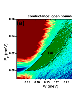
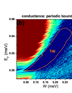
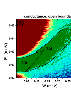
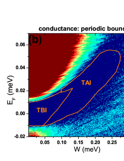
Let us start from the clean system with meV, which is topologically trivial. When disorder strength is tuned on gradually, as first found in Ref. Li09 , the system can evolve into TAI in a very large range in the parameter space, which is characterized by perfectly quantized conductance plateau as expected to be carried by the helical edge states. This disorder induced conductance plateau is contrary to the general intuition that disorder always tends to localize electronic states. Here we reconstruct the conductance diagram on the plane for a definite sample with the open boundary condition in Fig. 1 (a). To compare with the bulk transport mechanism, we also present the conductance diagram for the same sample with the periodic boundary condition in the transverse direction in Fig. 1 (b). Notice the conductance plateau in Fig. 1 (a) corresponds to a bulk mobility gap with in Fig. 1 (b). This confirms once again that the quantum transport in TAI is carried by helical edge statesLi09 ; Jiang2009 .
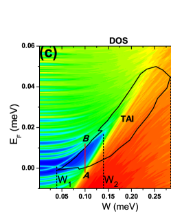
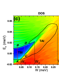
In order to relate the above transport properties to the developments of band structures of the sample, we present the arithmetic mean DOS of the same sample in Fig. 1 (c). The developments of energy levels with the increasing of disorder strength can be clearly illustrated. At small , the conduction and valance bands tend to get closer until they cross at meV, where a band inversion occurs. This gap closing and reopening indicates a topological quantum phase transition induced by disorderGroth2009 ; YYZhang2012 . This can be confirmed from Fig. 1 (a) that after , there emerges the conductance plateau. Soon after the gap re-opening in Fig. 1 (c), one may notice a small inconsistency between the angle-shaped boundary of conductance plateau (thick black line) and the opened gap (blue region between the bands). This can be simply attributed to different boundary conditions in the two calculations: the DOS was calculated from an isolated sample while the conductance was calculated in the presence of two leads connecting to the sample. This boundary condition sensitivity in weak disorder regime can also be observed in the same region Fig. 1 (b).
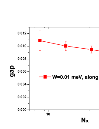
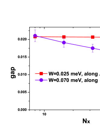
However, by comparing Fig. 1 (c) with the plateau region (enclosed by the thick black line) obtained from Fig. 1 (a), we can see that this disorder induced band inversion is not the whole story of the TAI: there is a level merging at meV after which the energy levels merge together without another gap reopening again. This level merging does not affect the quantized conductance at all. At a finite size (for example here), the full gap regime () between to (the blue region between and in Fig. 1 (c)) only constitutes a very small portion of the conductance plateau. To investigate the fate of this band gapped topological insulator regime, i.e. TBI, under the thermodynamic limit (), we plot the size dependence of the averaged gap size at meV (along line AB in Fig. 1 (c)) in Fig. 2. This curve is approximately linear with in logarithmic scale, therefore the gap decays slowly (logarithmically) with the increasing of sample size , suggesting that this small “TBI” region shrinks smaller or even vanishes in the thermodynamic limit.
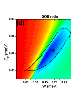
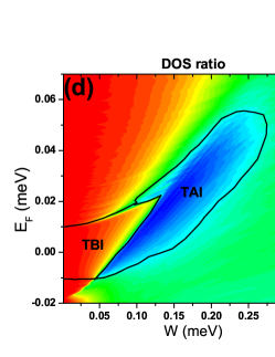
Most part of the conductance plateau in Fig. 1 corresponds to a region with a large bulk DOS . In other words, these topological states do not live in a bulk gap at all. From the plot of ratio in Fig. 1 (d), we can see that this region of TAI is related to extremely localized states with . From Fig. 1 (d), it is interesting to note that in the TAI region is even smaller (i.e., more localized) than any other region (even with larger ) in the plot range. This is consistent with the physical picture found in our previous workYYZhang2012 , that these extremely localized states (Anderson insulator) correspond to flat but densely distributed subbands (therefore contribute to DOS, but not to conductance). These flat subbands have trivial topological numbers, therefore they do not change the topological nature of nearby energy region. With open boundaries, helical edge states appear between adjacent flat subbands and contribute to the conductance . These subbands are so flat that their total measure on the energy axis is extraordinarily small, therefore there is always enough space to occupy helical edge states between them, in the case of an open boundary. In other words, the TAI phase lives in a bulk state of Anderson insulator (instead of band insulator), as the name suggests. The extremely localized nature of the bulk Anderson insulator also prohibits backscattering between edge states on opposite edges, therefore we call that the TAI is protected by a mobility gap instead of a band gap.
With further increasing of disorder strength , as in any lattice systems, the electronic states will finally be localized completely and the system becomes an Anderson insulator Hatsugai1999 , which happens after meV in the present system.
III.2 An inverted band
Now we turn to the case of an inverted band: meV, which is a TBI in the clean limit. From the conductance plateau in Fig. 3 (a) and (b), it seems that this phase diagram is quite simple: the topological phase characterized by helical edge states survives robustly until a complete collapse at a very large disorder meV. However, a detailed numerical calculation demonstrates that the regime of topological phase actually also consists of two parts: one is the TBI and the other is TAI. Although the conductance plateau in Fig. 3 (a) is continuous, the DOS can be used to distinguish the two phases very well. In the DOS plot in Fig. 3 (c), we can see the developments of energy levels under increasing of disorder strength . Note the conductance and valence bands merge at meV, which is much weaker than where the conductance plateau collapses.
We first concentrate on the conductance plateau region with , i.e., before the band merging, which is apparently a band insulator. As can be seen in Fig. 3 (c) for a definite size and disorder configuration, at weak disorder starting from , the bulk gap increases slowly with increasing disorder until , reflecting the band repelling of topological nontrivial bands under disorderYYZhang2012 . On the other hand, as the red curve with square dots in Fig. 4, the size dependence of the averaged gap at a definite (along line AB in Fig. 3 (c) ) indicates that it is a horizontal line with negligible statistical errors, suggesting a robust region of TBI independent of sample size and disorder configurations. After , the bulk gap begins to shrink, but the conductance plateau remains unchanged. In other words, TAI with quantized persists and finite gradually appears when . In Fig. 4, the gap size in this region for a definite (along line CD in Fig. 3 (c) ) as a function of sample size is plotted as the violet curve: it decays logarithmically. This simply suggests that in the thermodynamic limit, the region of the TBI is even smaller than that plotted in Fig. 3 for finite size . On the other hand, as discussed above, the TBI is always robust and well-defined before .
On the right side of the border between TBI and TAI, the phase possesses the typical characters of TAI: quantized conductance plateau living in a bulk mobility gap with nonzero DOS from extremely localized states. From the phase diagram in Fig. 3, It is interesting to notice that TAI phase (with quantized , finite and small ) still occupies a large portion of the conductance plateau. This comes from the localization of bulk sates near band edges under disorder. Therefore we emphasize that even tuning disorder on from an inverted band, the TAI also plays a very important role in the whole topological phase. As can be seen from Fig. 3, the boundary between the two topological phases is sharp and clear without any intermediate state, say, a metal phaseProdan2011 .
IV Summary and Discussions
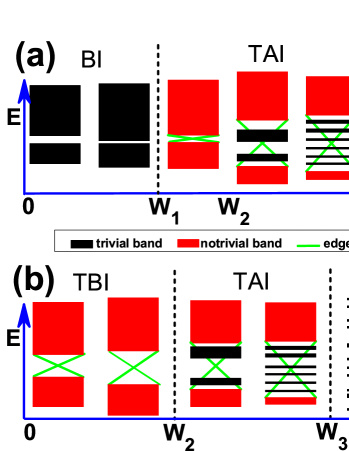
Now we can summarize the route towards localization schematically fora disordered quantum spin Hall system in Fig. 5. In the clean limit of , the electronic states form well-defined energy bands, and the band gap between the conduction and valence band are well defined. If we start from a conventional band insulator, as shown in Fig. 5 (a), weak disorder tends to shrink the bulk band gapGroth2009 ; YYZhang2012 ; DWXu . If the gap is small enough, then this disorder induced band attraction will eventually lead to a band closing at , after which edge states emerge in the re-opened gap. On the other hand, disorder destroys the translation invariance, making the energy band worse defined and split into more discrete energy levels. Around the band edges, these levels constitute to localized statesMott1968 ; Localization1993 . The calculation of a single impurity indicates that the in-gap bound states can be induced easily by a single impurity in the inverted band regimeJLu2011 . After , these localized states permeate into the bulk gap, leading to a well-defined TAI.
From this picture, we can see the condition for a stable disorder induced TAI phase. First, the clean limit gap should be sufficiently small to guarantee . Second, after , the in-gap bulk states should be sufficiently localized (or equivalently, sufficiently flat). From the viewpoint of momentum space, the in-gap states should be flat enough for edge states between them to show up. From the view point of real space, these states in the bulk should be localized enough to protect helical edge states from backscattering. This is why we call TAI a mobility gap protected topological insulating state, compared with TBI, an energy gap protected one. When we start from topological insulating phase, as in Fig. 5 (b), weak disorder tend to expel the conduction and valance bandsYYZhang2012 . Before the disorder decompose the energy bands into sufficiently discrete energy levels (), the system is still in a well-defined topological band insulating phase. After that, the bulk states near the band edges will be localizedMott1968 ; Localization1993 , and grow into the bulk gap to make a TAI phase.
In this work, we try to distinguish the topological insulating phases in 2D as a band insulator and an Anderson insulator. In Fig. 3 we define a border between TBI and TAI in the inverted band structure. This raises a question of whether they are physically distinct from each other by measuring the mobility gap or any other physical quantities. Usually temperature-dependencies of the bulk conductance are different between band insulators and Anderson insulators. With the help of thermal activation and phonons, the typical temperature dependence of conductivity for the band insulator is while that of the Anderson insulator is Mott1969 .
The energy scale of the two-dimensional mobility gap can be determined from capacity measurement as well as transport measurement in Corbino samples.Yang-97prl In the geometry of Corbino disk, edge transport is stuck around the concentric contacts, and the radial conductance measurement mainly probe the bulk properties. The mobility gap can be revealed by using capacitance-voltage and conductance measurement. In recent experiment in InAs/GaSb bilayers Du-13xxx , it is observed that the existence of quantized conductance in quantum spin Hall effect is accompanied by the appearance of the mobility gap. The measured capacitance shows clearly the gap opening between conduction and valance bands, and further opening of the mobility gap at lower temperatures. Coexistence of the mobility gap and the quantized conductance from helical edge states is characteristic of TAI. In this sense, the quantized conductance appears in the TAI regime.
Acknowledgements.
This work was supported by the Research Grant Council of Hong Kong under Grant No.: HKU 7051/11P. YYZ was also supported by NSFC under grant number: 11204294 and 973 Program Project No. 2013CB933304.References
- (1) M. Z. Hasan and C. L. Kane, Rev. Mod. Phys. 82, 3045 (2010).
- (2) X.-L. Qi and S.-C. Zhang, Rev. Mod. Phys. 83, 1057 (2011).
- (3) S. Q. Shen, Topological Insulators (Springer-Verlag, Berlin, 2012).
- (4) C. L. Kane and E. J. Mele, Phys. Rev. Lett. 95, 146802 (2005).
- (5) A. Bernevig, T. Hughes and S. C. Zhang, Science 314, 1757 (2006).
- (6) B. Zhou, H. Z. Lu, R. L. Chu, S. Q. Shen, and Q. Niu, Phys. Rev. Lett. 101, 246807 (2008).
- (7) M. König, S. Wiedmann, C. Brüne, A. Roth, H. Buhmann, L. W. Molenkamp, X. L. Qi and S. C. Zhang, Science 318, 766 (2007).
- (8) A. Roth, C. Brüne, H. Buhmann, L. W. Molenkamp, J. Maciejko, X.-L. Qi, S.-C. Zhang, Science 325, 294 (2009).
- (9) I. Knez, R. R. Du, and G. Sullivan, Phys. Rev. Lett. 107, 136603 (2011).
- (10) L. J. Du, I. Knez, G. Sullivan, and R. R. Du, arXiv: 1306.1925.
- (11) J. Li, R.-L. Chu, J. K. Jain and S.-Q. Shen, Phys. Rev. Lett. 102, 136806 (2009).
- (12) H. Jiang, L. Wang, Q.-F. Sun and X. C. Xie, Phys. Rev. B 80, 165316 (2009).
- (13) C. W. Groth, M. Wimmer, A. R. Akhmerov, J. Tworzydło and C. W. J. Beenakker, Phys. Rev. Lett. 103, 196805 (2009).
- (14) H.-M. Guo, G. Rosenberg, G. Refael and M. Franz, Phys. Rev. Lett. 105, 216601 (2010).
- (15) E. Prodan, T. L. Hughes and B. A. Bernevig, Phys. Rev. Lett. 105, 115501 (2010).
- (16) E. Prodan, Phys. Rev. B 83, 195119 (2011).
- (17) Y.-X. Xing, L. Zhang and J. Wang, Phys. Rev. B 84, 035110 (2011).
- (18) A. Yamakage, K. Nomura, K.-I. Imura, and Y. Kuramoto, J. Phys. Soc. Jpn. 80 053703 (2011).
- (19) S. Ryu and Kentaro Nomura, Phys. Rev. B 85, 155138 (2012).
- (20) D. Xu, J. Qi, J. Liu, V. Sacksteder, X. C. Xie and H. Jiang, Phys. Rev. B 85, 195140 (2012).
- (21) J.-T. Song, H.-W. Liu, H. Jiang, Q.-F. Sun and X.-C. Xie, Phys. Rev. B 85, 195125 (2012).
- (22) Y.-Y. Zhang, R.-L. Chu, F.-C. Zhang and S.-Q. Shen, Phys. Rev. B 85, 035107 (2012).
- (23) A. Weisse, G. Wellein, A. Alvermann and H. Fehske, Rev. Mod. Phys. 78, 275 (2006).
- (24) S. Q. Shen, W. Y. Shan, and H. Z. Lu, SPIN 1, 33 (2011).
- (25) M. König, H. Buhmann, L. W. Molenkamp, T. Hughes, C.-X. Liu, X.-L. Qi and S.-C. Zhang, J. Phys. Soc. Jpn. 77, 031007 (2008).
- (26) H. Z. Lu, W. Y. Shan, W. Yao, Q. Niu, and S. Q. Shen, Phys. Rev. B 81, 115407 (2010).
- (27) S. Datta, Electronic Transport in Mesoscopic Systems (Canmbridge University Press, Cambridge, U.K., 1995).
- (28) Y. Hatsugai, K. Ishibashi and Y. Morita, Phys. Rev. Lett. 83, 2246 (1999).
- (29) N. F. Mott, J. Non-Crysr. Solids 1, 1 (1968).
- (30) B. Krameri and A. MacKinnon, Rep. Prog. Phys. 56, 1469 (1993).
- (31) J. Lu, W.-Y. Shan, H.-Z. Lu, and S.-Q. Shen, New J. Phys. 13, 103016 (2011).
- (32) N. F. Mott, Phil. Mag. 19, 835 (1969).
- (33) M. Yang, C. Yang, B. Bennett, and B. Shanabrook, Phys. Rev. Lett. 78, 4613-4616 (1997).