A nearly relaxation-free opto-electronic memory from ultra-thin graphene-MoS2 binary hybrids
Ultra-thin planar heterostructures of graphene and other two-dimensional crystals have recently attracted much interest. Very high carrier mobility in a graphene-on-boron nitride assembly is now well-established deanNatnano2010 ; zomerAPL2011 , but it has been anticipated that appropriately designed hybrids could perform other tasks as well novoselovNATURE2012 . A heterostructure of graphene and molybdenum disulphide (MoS2) is expected to be sensitive to photo illumination due to the optical bandgap in MoS2 heinzPRL2010 . Despite significant advances in device architectures with both graphene xiaNatNano2009 ; xiaNL2009 ; ghoshAPL2010 ; dassarmaRMP2011 and MoS2 radisavljevicNatnano2011 ; cnrraoACSNANO2012 ; zongyouACSnano2011 ; leeNL2012 ; branimirACSnano2011 , binary graphene-MoS2 hybrids have not been realized so far, and the promising opto-electronic properties of such structures remain elusive. Here we demonstrate experimentally that graphene-on-MoS2 binary heterostructures display an unexpected and remarkable persistent photoconductivity under illumination of white light. The photoconductivity can not only be tuned independently with both light intensity and back gate voltage, but in response to a suitable combination of light and gate voltage pulses the device functions as a re-writable optoelectronic switch or memory. The persistent, or ‘ON’, state shows virtually no relaxation or decay within the the experimental time scales for low and moderate photoexcitation intensity, indicating a near-perfect charge retention. A microscopic model associates the persistence with strong localization of carriers in MoS2. These effects are also observable at room temperature, and with chemical vapour deposited graphene, and hence are naturally scalable for large area applications.
Many optical switches and memories rely on persistent photoconductivity (PPC) where electromagnetic excitation shifts the electrical resistance of the host material to a slowly relaxing state. Traditionally, PPC is observed in compound semiconductors, alloys and heterojunctions kastalskySSC1984 ; nathanSSE1986 ; queisserPRB1986 , but more recently, assemblies of carbon-based nano-materials julienADMA2006 have also received considerable interest. External tunability of the PPC, for example with a gate, makes such designs particularly attractive for switching and read-write memory applications, as demonstrated with nanotubes dispersed in photoactive polymers julienADMA2006 .
PPC has so far not been realized in graphene-based field-effect devices, although such devices would readily benefit from strong coupling to light over a wide band of wavelengths in graphene dawlatyAPL2008 ; nairSci2008 , and fast recombination life times georgeNL2008 ; urichNL2011 ; songNL2011 ; gaborSci2011 , along with gate-tunability, miniaturization and ability to pattern over a large area ghoshAPL2010 . A significant improvement in photoconductivity of graphene has been achieved by combining graphene with other light absorbing materials such as quantum dots konstantatosNatnano2012 and chromophores myungwoongNL2012 . This indicates that exotic optoelectronic response could be engineered in graphene-based hybrids with an appropriate choice of complementary materials.
Molybdenum disulphide (MoS2) is intrinsically responsive to light, owing to its bandgap which increases from about eV (indirect) in bulk/multilayer MoS2 to eV (direct) for a single molecular layer heinzPRL2010 . MoS2 can also be exfoliated mechanically, and can be stabilized in single or multilayered form on insulating substrate radisavljevicNatnano2011 ; ghatakACSnano2011 . This opens up an avenue to create planar heterojunctions of Graphene and MoS2 through physical proximity. In this work we have explored the opto-electronic properties of such planar graphene-MoS2 hybrids.

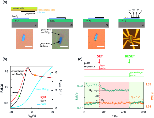
The device architecture, process flow and measurement layout are shown in Fig. 1a. We have used single layer graphene and multilayer ( molecular layers) MoS2, both of which were obtained via mechanical exfoliation, and subsequently overlayed by vertical alignment (see methods for details). This technique is same as that for overlaying exfoliated graphene on BN microflakes, which provides a trap-free high-quality interface zomerAPL2011 ; deanNatnano2010 , essential for the present experiments. In all devices, the MoS2 was exfoliated on a SiO2/p+-Si substrate, and graphene was then transferred on top of MoS2. The layout of the electrical leads can be designed to measure the four-probe resistance () of graphene (on MoS2), and two-probe conductance () of the underlying MoS2 (that is not covered by graphene) simultaneously. The devices were loaded on a variable-temperature cryostat along with a commercial white light emitting diode (LED) to provide the photo excitation.
Typical gate voltage () characteristics, recorded at 110 K, of the graphene (on-MoS2) and bare MoS2 regions are shown in Fig. 1b. The characteristics of graphene, even in the absence of light (black trace in Fig. 1b), was found to be very different from the usual gate transfer characteristics of graphene on an insulating dielectric such as SiO2. The normal ‘bell-shaped’ characteristics are observed only at large negative , whereas for positive , becomes increasingly insensitive to . This asymmetric can be readily understood by referreing to the characteristics of the underlying MoS2 (cyan trace). Since we used natural type MoS2 for exfoliation, the MoS2 channel starts populating only for , where is the threshold voltage for conduction. Typically, lies between V to V for most multilayer MoS2 channels that we have measured ghatakACSnano2011 . Here, when , MoS2 turns ‘ON’ (conducting), and screens the gate voltage applied to graphene. Two points need to be noted here: First, for the device presented here, the Dirac point ( V) lies close to , which is a coincidence, and the two voltage scales can be very different (e.g. see Fig. 4a, where V). Second, for , where MoS2 behaves as a (poor) dielectric, it does not form a parallel conducting channel.

We now illuminate the device by forward biasing a white LED with a current . The red trace in Fig. 1b was recorded while the device was illuminated continuously with mA corresponding to a photoexcitation power of pW/m2. Note that there is a pronounced effect only on the negative side of the where an increase in is observed in the presence of light. This negative photoconductivity can be understood as a transfer of the photogenerated electrons inside MoS2 to graphene under the influence of a negative . Since graphene is hole-doped in this regime, addition of electrons increases . However, when , the bands in MoS2 stay flat due to its near-metallic nature. This suppresses the transfer of photoexcited carriers from MoS2 to graphene.
The response of the hybrid was found to be significantly more striking when we used pulsed, instead of continuous, photoexcitation. Fig. 1c shows the response of to a sequence of light and gate voltage pulses for two different on opposite sides of (denoted by the markers in Fig. 1b). At V (i.e., ) the light pulse ( pulse height = 5 mA, pulse width s) induces a transient-like behavior in . It rises instantaneously from its dark state value (), and then decays over few tens of seconds to a higher final value (), indicating a persistent negative photoconductivity. The magnitude of PPC is defined as . On the other hand, it is clear that when ( V), the light pulse has no measurable effect on , in agreement with experiments performed with continuous illumination. This sensitivity of the PPC to the relative positions of and allowed us to develop a strategy to erase the PPC in our devices. By introducing a pulse in we were able to ‘reset’ the device to its original dark state resistance from the persistent state. The trace corresponding to V in Fig. 1c demonstrates this switching. A gate voltage of pulse height and duration s restored to within a timescale limited by the measurement/pulsing electronics. Typically, we used V, so that . We would like to point out that our control experiments with MoS2 and graphene separately show no clear evidence of PPC in both cases (see Fig. S1 in supplementary information (SI)).
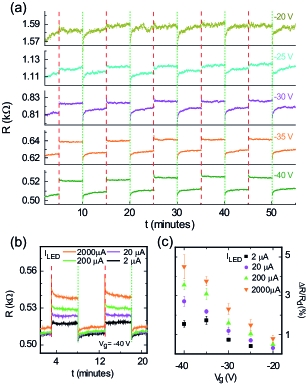
Fig. 2a shows the evolution of the PPC cycles with (). It is clear that is largest for V, and almost vanishes when is increased to V. At any , the ‘light set - voltage reset’ cycles could be performed over days with better than 95% accuracy in recovering the PPC magnitude. The PPC magnitude also decreases when the intensity of light pulse is reduced, as can be seen in Fig. 2b, where we varied over three decades of magnitude. The results of Figs. 2a and 2b are summarized in Fig. 2c where is plotted as a function of for various light intensities. is found to be as large as 5% at T K (similar values of PPC can be achieved at room temperature by making more negative). It is perhaps not surprising that the PPC magnitude depends on the light intensity, however its extreme sensitivity to gate voltage opens up the possibility of creating a new class of electrically tunable optoelectronic devices.
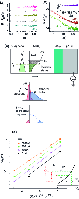
A key feature of the switching cycles in Fig. 2 is the absence of a time-dependent decay in the photoconductivity in the persistent state, particularly at low photo-illumination intensity (Fig. 2b). In Fig. 3a we have plotted the photoconductivity in the persistent state in one of the cycles after a low-intensity pulse (A) for three different . The PPC shows no decay with time over three decades irrespective of , remaining essentially constant even when we monitored it over more than 10 hours (inset of Fig. 3b, here A and V have been used). At higher (A), we do observe a logarithmic decay at times s, although at long times photoconductivity becomes nearly time-independent again. This is illustrated in Fig. 3b with PPC relaxation for A pulses.

The near-absence of time decay of the persistent state suggests a strong potential barrier that prohibits recombination of electron and holes created on photo-illumination. To understand this we note that the majority carriers (electrons) in natural MoS2 flakes are strongly localized ghatakACSnano2011 , and display Mott-type variable range hopping transport when is reduced to the conduction threshold . Thus our graphene-MoS2 hybrid behaves as a heterojunction of a doped conducting system (graphene) and a semiconductor (MoS2) where the carriers are localized, and trapped in potential wells that separate them from the conducting region queisserPRB1986 . represents the gate voltage at which the Fermi energy () approaches the mobility edge (). The distribution of carriers queisserPRB1986 right after the light pulse (t = 0) is shown in the schematic of Fig. 3c. The electrons are swept towards the graphene-Mo interface, and addition of electrons to the p-doped graphene results in an immediate increase in . The holes remain trapped in MoS2, but after light is switched off the hole distribution is modified by: (1) quantum tunneling mediated electron-hole recombination, and (2) thermal excitation of holes from the graphene to MoS2. The PPC then determined by the excess electron density, , left in graphene at time after the illumination is turned off. As derived in the supplementary information (Eq. S5), can be expressed as,
| (1) |
where is a logarithmically decaying function when the initial hole distribution is assumed continuous and uniform. However, constant for isolated local accumulation of holes far away from the graphene-MoS2 interface, as the recombination time becomes exponentially long. This is consistent with the observation that decay-free PPC occurs only for weak illumination, or at long time when the illumination is strong. Strong localization in MoS2 makes recombination via quantum tunneling or thermal activation virtually ineffective, and the equilibrium is restored only by lifting to , which provides the “erasing” mechanism of the PPC as reverts to its dark-state resistance.
To address the -dependence, we estimated from the asymptotic time-independent value of and the equivalent shift () in the gate voltage. The scheme is shown in the inset of Fig. 3d, where could be evaluated directly from the experimentally measured characteristics (black trace in Fig. 1b). Due to the linear bands in graphene (see SI for details), we find:
| (2) |
where . Here, is the effective capacitance between the silicon backgate and graphene and is the Fermi velocity in graphene. The exponential increase in with is clearly observed for different photoexcitations in Fig. 3c. Experimentally, we get which indicates that is about a factor of smaller than the bare capacitance of 285 nm SiO2 that we used as gate dielectric. This can be readily attributed to the quantum capacitance of the MoS2 film which acts as a ‘leaky’ capacitor. Note that, if we consider this modified value of the capacitance, we find that the mobility of graphene in our sample is cm2V-1s-1 which is higher than that typically obtained for exfoliated graphene on bare SiO2 substrates.
Finally, we ask three important questions: (i) whether the PPC can be observed in other graphene devices, particularly for large area scalability (ii) can the devices work at room temperature, and (iii) how stable are the devices over long-time operation (suitable for non-volatile memory applications).

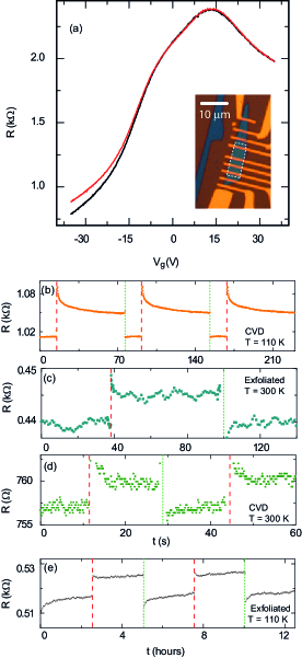
We have fabricated similar devices by transferring graphene grown via chemical vapor deposition (CVD) onto exfoliated multilayer MoS2. In the inset of Fig. 4a, we show an optical image of one such device. The curves of the device with and without light are shown in Fig. 4a. The CVD-device behaves very similarly to the exfoliated device, albeit with a smaller magnitude of for the same intensity of illumination. This might be correlated with the lower mobility and higher disorder typically associated with CVD growth matteviJMC2011 ; atinAPL2010 . Nevertheless, the switching action shown in Fig. 4b confirms PPC. Note that a recent report has shown that large scale CVD growth of MoS2 is possible on graphene substrates shiNL2012 , thereby paving new ways for large area device designs.
In Figs. 4c and 4d, we show that PPC is observable even at room temperature for both exfoliated and CVD-graphene devices. However, thermal broadening reduces the threshold for conduction in MoS2, which makes the effect clearly observable only at large negative . For example, the data shown in Fig. 4c corresponds to V. Correspondingly, the gate voltage pulse applied ( V) for recovery was also large. Fig. 4e shows switching cycles in the exfoliated device over a long period of time extending several hours. It confirms that such devices can be promising for nonvolatile memory applications.
I Methods
Transfer procedure for laying graphene on MoS2: Here we follow a similar procedure to Zomer et al. zomerAPL2011 . A piece of glass is covered with a transparent tape and coated with a polymer such as PMMA or EL-9. Graphene is exfoliated onto this substrate. Separately, MoS2 is transferred to an Si/SiO2 substrate by standard mechanical exfoliation and placed on the micromanipulator stage of an MJB3 mask aligner with a custom built heater. The graphene flake, now on a transparent substrate, is positioned upside down and aligned with the MoS2 flake using the microscope of the aligner. The two are brought into contact at an elevated temperature (C) as a result of which graphene, along with the polymer is transferred onto MoS2. The polymer is later washed off with acetone.
Device fabrication and measurement: Once transferred onto MoS2, graphene (exfoliated or CVD-grown) is etched into a desired shape by oxygen plasma. Contacts are drawn using standard e-beam lithography and metallization is done with Ti/Au (15 nm/45 nm) or Cr/Au (15 nm/45 nm). In devices where contacts need to be put on MoS2 also, we use Au as the contact metal. Measurements are done on graphene using a standard 4-probe lock-in technique. A commercial white LED is used as the light source.
CVD growth: The CVD-graphene reported in this study was synthesized by low-pressure CVD (base pressure of 1 Torr). 25 m thick copper foils were annealed at 1000 ∘C for 5 minutes under a H2 flow of 50 sccm to reclaim the pure metal surface. CH4 and H2 were then introduced at a rate of 35 sccm and 2 sccm for a growth time of 30 s. The reactor was cooled down to room temperature at a cooling rate of 8∘C/minute under a 1000 sccm flow of H2.
II Acknowledgement
We acknowledge the Department of Science and Technology (DST) for a funded project. S.R. acknowledges support under Grant No. SR/S2/CMP-02/2007.
References
- (1) Dean., C. et al. Boron nitride substrates for high-quality graphene electronics. Nature Nanotech. 5, 722–726 (2010).
- (2) Zomer, P. J., Dash, S. P., Tombros, N. & van Wees, B. J. A transfer technique for high mobility graphene devices on commercially available hexagonal boron nitride. Appl. Phys. Lett. 99, 232104 (2011).
- (3) Novoselov, K. S. et al. A roadmap for graphene. Nature 490, 192–200 (2012).
- (4) Mak, K. F., Lee, C., Hone, J., Shan, J. & Heinz, T. F. Atomically thin MoS2: A new direct-gap semiconductor. Phys. Rev. Lett. 105, 136805 (2010).
- (5) Xia, F., Mueller, T., Lin, Y.-m., Valdes-Garcia, A. & Avouris, P. Ultrafast graphene photodetector. Nature Nanotech. 4, 839–843 (2009).
- (6) Xia, F. et al. Photocurrent imaging and efficient photon detection in a graphene transistor. Nano Lett. 9, 1039–1044 (2009).
- (7) Ghosh, S., Sarker, B. K., Chunder, A., Zhai, L. & Khondaker, S. I. Position dependent photodetector from large area reduced graphene oxide thin films. Appl. Phys. Lett. 96, 163109 (2010).
- (8) Das Sarma, S., Adam, S., Hwang, E. H. & Rossi, E. Electronic transport in two-dimensional graphene. Rev. Mod. Phys. 83, 407–470 (2011).
- (9) Radisavljevic, B., Radenovic, A., Brivio, J., Giacometti, V. & Kis, A. Single-layer MoS2 transistors. Nature Nanotech. 6, 147–150 (2011).
- (10) Late, D. J., Liu, B., Matte, H. S. S. R., Dravid, V. P. & Rao, C. N. R. Hysteresis in single-layer MoS2 field effect transistors. ACS Nano 6, 5635–5641 (2012).
- (11) Yin, Z. et al. Single-layer MoS2 phototransistors. ACS Nano 6, 74–80 (2012).
- (12) Lee, H. S. et al. MoS2 nanosheet phototransistors with thickness-modulated optical energy gap. Nano Lett. 12, 3695–3700 (2012).
- (13) Radisavljevic, B., Whitwick, M. B. & Kis, A. Integrated circuits and logic operations based on single-layer MoS2. ACS Nano 5, 9934–9938 (2011).
- (14) Kastalsky, A. & Hwang, J. Study of persistent photoconductivity effect in n-type selectively doped AlGaAs/GaAs heterojunction. Solid State Commun. 51, 317 – 322 (1984).
- (15) Nathan, M. I. Persistent photoconductivity in AlGaAs/GaAs modulation doped layers and field effect transistors: A review. Solid-State Electron. 29, 167 – 172 (1986).
- (16) Queisser, H. J. & Theodorou, D. E. Decay kinetics of persistent photoconductivity in semiconductors. Phys. Rev. B 33, 4027–4033 (1986).
- (17) Borghetti, J. et al. Optoelectronic switch and memory devices based on polymer-functionalized carbon nanotube transistors. Adv. Mater. 18, 2535–2540 (2006).
- (18) Dawlaty, J. M. et al. Measurement of the optical absorption spectra of epitaxial graphene from terahertz to visible. Appl. Phys. Lett. 93, 131905 (2008).
- (19) Nair, R. R. et al. Fine structure constant defines visual transparency of graphene. Science 320, 1308 (2008).
- (20) George, P. A. et al. Ultrafast optical-pump terahertz-probe spectroscopy of the carrier relaxation and recombination dynamics in epitaxial graphene. Nano Lett. 8, 4248–4251 (2008).
- (21) Urich, A., Unterrainer, K. & Mueller, T. Intrinsic response time of graphene photodetectors. Nano Lett. 11, 2804–2808 (2011).
- (22) Song, J. C. W., Rudner, M. S., Marcus, C. M. & Levitov, L. S. Hot carrier transport and photocurrent response in graphene. Nano Lett. 11, 4688–4692 (2011).
- (23) Gabor, N. M. et al. Hot carrier-assisted intrinsic photoresponse in graphene. Science 334, 648–652 (2011).
- (24) Konstantatos, G. et al. Hybrid graphene-quantum dot phototransistors with ultrahigh gain. Nature Nanotech. 7, 363–368 (2012).
- (25) Kim, M., Safron, N. S., Huang, C., Arnold, M. S. & Gopalan, P. Light-driven reversible modulation of doping in graphene. Nano Lett. 12, 182–187 (2012).
- (26) Ghatak, S., Pal, A. N. & Ghosh, A. Nature of electronic states in atomically thin MoS2 field-effect transistors. ACS Nano 5, 7707–7712 (2011).
- (27) Mattevi, C., Kim, H. & Chhowalla, M. A review of chemical vapour deposition of graphene on copper. J. Mater. Chem. 21, 3324–3334 (2011).
- (28) Pal, A. N., Bol, A. A. & Ghosh, A. Large low-frequency resistance noise in chemical vapor deposited graphene. Appl. Phys. Lett. 97, 133504 (2010).
- (29) Shi, Y. et al. Van der Waals epitaxy of MoS2 layers using graphene as growth templates. Nano Lett. 12, 2784–2791 (2012).