Second Harmonic Generation in Photonic Crystal Cavities in (111)-Oriented GaAs
Abstract
We demonstrate second harmonic generation at telecommunications wavelengths in photonic crystal cavities in (111)-oriented GaAs. We fabricate 30 photonic crystal structures in both (111)- and (100)- oriented GaAs and observe an increase in generated second harmonic power in the (111) orientation, with the mean power increased by a factor of 3, although there is a large scatter in the measured values. We discuss possible reasons for this increase, in particular the reduced two photon absorption for transverse electric modes in (111) orientation, as well as a potential increase due to improved mode overlap.
pacs:
42.70.Qs, 78.67.Hc, 42.65.Ky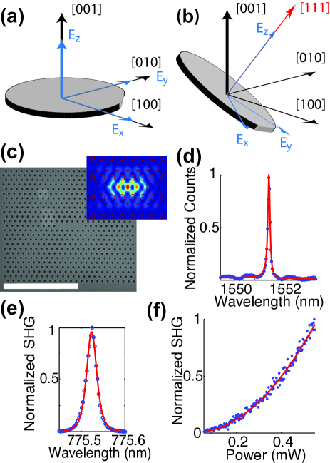
Low mode-volume, high quality (Q) factor optical microcavities are promising for nonlinear optical devices, as they have the potential to reach similar conversion efficiencies to traditional optical cavities, but in significantly more compact devices. In particular, if the optical mode volume becomes small compared to the material nonlinear coherence length, the phase matching condition is replaced by the requirement of large mode overlap between the relevant optical modes Rodriguez et al. (2007). This is particularly useful in the case of III-V semiconductors such as GaAs, GaP and InP, as these materials have a very high second order nonlinearity, but do not exhibit birefringence. This makes phasematching of bulk III-V semiconductors challenging, and typically quasi-phasematching or additional birefringent materials are employed. Quasi-phasematching these materials poses additional challenges as, unlike frequently used LiNbO3, III-Vs are not ferroelectric and require wafer bonding or epitaxial growth for periodic poling Eyres et al. (2001). Conversely, integration of III-V materials with optical microcavities is relatively easy due to the ease of fabrication using semiconductor processing. III-V semiconductors also allow integration of active gain media such as quantum dots or quantum wells Rivoire et al. (2011); Buckley et al. (2012); Ota et al. (2013), as well as potential on-chip integration with detectors, switches and modulators.
Experimentally, high efficiency, low power nonlinear processes in resonant microcavities have been demonstrated, in particular second harmonic generation in microdisks Kuo and Solomon (2012) and microrings Levy et al. (2011), as well as second harmonic generation and sum frequency generation in photonic crystal cavities McCutcheon et al. (2007); Rivoire et al. (2009); Diziain et al. (2013). Millimeter sized lithium niobate microdisks have also been used for high efficiency second harmonic generation and ultra-low threshold optical parametric oscillators (OPOs) Ilchenko et al. (2003); Fürst et al. (2010); Förtsch et al. (2013). The efficiency of the conversion process is proportional to the quality factors and spatial overlap integral of the three modes involved Liscidini and Andreani (2004); Rodriguez et al. (2007). In the case of second harmonic generation in photonic crystal cavities, the experimentally achieved efficiency of the processes has been limited by the difficulty of engineering multiple high quality factor modes with a high degree of overlap McCutcheon et al. (2007); Rivoire et al. (2009); Diziain et al. (2013). This difficulty arises because the bandgap of photonic crystals does not span a sufficiently large frequency range for processes, and there are no significant higher order bandgaps. This means that only one of the modes of the photonic crystal cavity in the process is well defined and has high Q. For example, in experimentally demonstrated second harmonic generation in three hole defect (L3) photonic crystal cavities, the pump is coupled to the high Q fundamental cavity mode. Previous work indicates that second harmonic generation in photonic crystal cavities is primarily due to the bulk rather than a surface effect (even in materials where the generated second harmonic is above the bandgap and absorbed, )McCutcheon et al. (2007); Rivoire et al. (2009). This suggests that the second harmonic couples to leaky air band modes perturbed by the presence of the cavity McCutcheon et al. (2007); Rivoire et al. (2009); Buckley et al. (2012); Diziain et al. (2013), which have low Q factors, and potentially low overlap with the fundamental mode. In order to improve the efficiency, there have been several proposals for designing photonic crystal cavities with multiple high Q resonances and large frequency separations Zhang et al. (2009); Burgess et al. (2009); Thon et al. (2010); Rivoire, Buckley, and Vučković (2011a, b).
Additional complications in designing nonlinear cavities in III-V semiconductors arise due to the symmetry of the tensor; the only nonzero elements of the bulk have , where and are directions along the [100], [010] and [001] crystal axes. Furthermore, the mode overlap is proportional to , where is a component of the electric field and the numeric subscript describes a distinct mode in a three wave mixing process. Spatially anti-symmetric products of the three field components have zero overlap. The vertical symmetry of the photonic crystal cavity forces all modes to be either primarily transverse electric (TE) -like or transverse magnetic (TM) -likeJoannopoulos et al. (2011). For a TE-like mode, , and obey even symmetry in the vertical direction about the center of the slab while at the central plane and are anti-symmetric about this plane (where we define as the direction normal to the wafer, and and to be in the plane of the wafer). For TM-like modes, , and obey even symmetry in the vertical direction about the center of the slab while at the central plane and are anti-symmetric about this plane. Examining the mode overlap integral reveals that for the process of second harmonic generation, a TE-like mode may only couple to a TM-like mode if the wafer is normal to the [100], [010] or [001] (equivalent) directions, as in standard (001) oriented wafers Rivoire et al. (2009). This is illustrated in Fig. 1 (a). The consequence of this is that both high Q TE-like and TM-like modes must be engineered for second harmonic generation in suspended photonic crystals on this substrate, which is challenging as nearly all planar photonic crystals only have a bandgap for TE polarization (with the exception of a few recent demonstrations Takayama et al. (2005); McCutcheon et al. (2011), which require either complex 2D patterns or thick 1D structures, thereby making fabrication more challenging ). However, if the wafer is cut such that the plane of the wafer is normal to a different crystallographic direction, the and directions in the plane of the wafer may have components along each of the [100], [010] and [001] directions, and in this case TE-TE coupling between modes may be allowed. For example, in the case of (111) oriented III-Vs, illustrated in Fig. 1 (b), such TE-TE mode coupling is allowed. This opens up additional degrees of freedom for engineering photonic crystal cavities for frequency conversion Rivoire, Buckley, and Vučković (2011b), as all three modes in a three wave mixing process may now have either TE-like or TM-like symmetry.
In order to achieve efficient nonlinear frequency conversion, it is also desirable to choose a semiconductor with a transparency window that overlaps well with the experimental frequencies. GaP has a large bandgap and has been demonstrated as a high-efficiency nonlinear source of visible frequencies Rivoire et al. (2009), but is challenging to grow in (111) orientation. On the other hand, GaAs has a strong nonlinearity, is easier to grow in (111) crystal orientation, and is compatible with bright gain media such as InGaAs quantum wells, and efficient quantum emitters, such as InAs quantum dots Rivoire et al. (2011); Ota et al. (2013). However, GaAs has a smaller bandgap than GaP, and suffers from a large two photon absorption at telecommunications wavelengths, as well as linear absorption of visible wavelengths. Moreover, due to the tensor nature of the nonlinear properties, the two photon absorption of TE modes in (111) GaAs is several times smaller than in (001) GaAs Dvorak et al. (1994).
In order to demonstrate the improvement of nonlinear frequency conversion in nanophotonic structures by controlling the crystal orientation of the underlying material, we fabricate L3 photonic crystal cavities in (001) and (111) GaAs and compare second harmonic generation in both. Photonic crystal cavities were fabricated in 165 nm thick (001) and (111) GaAs membranes grown on a thick AlGaAs sacrificial layer (1 m thick in the (001) sample, 0.8 m thick in the (111) sample) on n-type doped substrates. The (111)B GaAs substrate was off-oriented by 2∘ towards [2-1-1]. The cavities were fabricated using e-beam lithography to define the pattern, followed by dry etching and HF wet etching to remove the sacrificial layer. An SEM of a fabricated device is shown in Fig. 1 (c). The fabricated structures had lattice constant = 460-470 nm and hole radius r/a = 0.28. The electric field of the fundamental mode of this cavity is shown inset in the figure, and was simulated by 3D finite difference time domain (FDTD) method. Fabricated photonic crystal cavities were all characterized experimentally at the fundamental (1st harmonic) wavelength with a broadband LED light source using a cross polarized reflectivity method Altug and Vuckovic (2005). The spectrum for the structure shown in Fig. 1 (c), measured by this method, is shown in Fig. 1 (d) with a Q factor of 10,000.
To perform second harmonic generation, a tunable CW telecommunications wavelength (1465-1575 nm) laser is reflected from a 50-50 beamsplitter and coupled to the high-Q fundamental cavity mode at normal incidence with a high numerical aperture objective lens. The second harmonic emission is collected through the same objective and passes through the beamsplitter to be measured on a liquid nitrogen cooled Si CCD spectrometer Rivoire et al. (2009). The tunable laser is scanned across the cavity resonance, and the maximum counts measured on the spectrometer for each laser wavelength are recorded. The value in counts/second was calibrated in order to calculate actual powers. An example of such a spectrum for the cavity in (111) GaAs measured shown in Fig. 1 (c) at 600 W pump power is shown in Fig. 1 (e), the red line is a fit to a Lorentzian squared with Q factor of 10,000. The second harmonic power dependence on input power can be recorded by varying the laser power at a particular wavelength; the resulting curve for the same cavity is shown in part (f), with a quadratic fit in red. Since the generated second harmonic is above the GaAs bandgap, the process efficiency is greatly reduced by the two photon absorption of the pump and linear absorption of the second harmonic; this is indicated by the fact that the measured power is significantly lower than that measured from similar cavities in GaP, despite the relatively higher nonlinearity of GaAs Shoji et al. (1997). Since at low powers the measured second harmonic versus pump power is quadratic and the efficiency versus pump power is approximately linear, in this power regime we can obtain the (constant) conversion efficiency per Watt of input pump power for each structure. The maximum low power conversion efficiency per Watt measured in a (111)-GaAs structure was 0.002 %/W (not accounting for in/out – coupling losses), which is 450 times lower than the measured conversion efficiency per Watt in GaP photonic crystal cavities.
Next, we compare the second harmonic spectra for similar L3 cavities in (111) and (001) GaAs, in order to demonstrate the difference in the second harmonic process in the two orientations for input powers leading to collected second harmonic powers in the pW range. We expect to observe a difference in the measured second harmonic power for fixed pump power, due to differences of the nonlinear optical interaction strengths and of the two-photon absorption coefficients between the two samples, although this experiment will not distinguish between the two effects. Around 30 cavities were fabricated for both (111) and (001) GaAs. The input power was kept at 600 W, where the second harmonic generation (SHG) versus pump curve was still quadratic for the case of (111) GaAs, as in Fig. 1 (e), but the power was high enough that second harmonic signal could be measured for most cavities. For (001) GaAs this may have already been in the strong nonlinear absorption regime due to the higher two photon absorption, however, below this power the second harmonic power was too low to measure for a significant number of structures in the (001) orientation, and therefore we chose to measure at 600 W in order to keep these structures in our sample. We therefore do not quote low power conversion efficiency for both but rather measure second harmonic power at 600 W. For each photonic crystal cavity, the tunable laser was scanned across the resonance. Second harmonic power was were plotted versus wavelength, and the peak value was recorded. Table 1 summarizes the results, which indicate higher efficiency SHG in the (111) orientation. A large structure to structure variation was observed, and is possibly due to the high sensitivity of air band mode frequencies to structure parameters, as well as variations in in- and out-coupling efficiency. In order to try to suppress this variation, we also fabricated perturbed L3 photonic crystal cavities buc . However, we still observed significant scattering of values. Since this scattering was less severe in the case of GaP cavities in previous studies Rivoire et al. (2009) (e.g. allowing a noticeable dependence on in plane cavity rotation), we suggest that the absorption contributes to the high sensitivity of measured powers. The results for (001)-oriented GaAs are statistically enhanced by the fact that there were several cavities in that orientation for which we could not measure any SHG, perhaps because the efficiency was too low, and these were not included in the results. Different rotations relative to the crystal axes were also fabricated, however, the variation from structure to structure was larger than any rotation variation that we could measure. Therefore, we include structures of all rotations in the table. The quality factor of the structures measured was between 8,000 and 13,000, and no significant dependence on Q factor was found in this range. We attribute this to the fact that although the conversion efficiency increases with increase in Q factor, the coupling efficiency decreases with increasing Q factor, and in this range the two effects cancel. The increase in the SHG in (111) cavities relative to (001) cavities may be a combination of the smaller two-photon absorption in (111) GaAs and the possible better overlap between the fundamental L3 cavity mode and air band modes, due to the possibility of coupling to TE modes, as explained above. FDTD simulations of the potential contributing air band modes Buckley et al. (2012) were used for calculations of the mode overlap, and indicate that this overlap can be improved or reduced with a change in wafer orientation by up to an order of magnitude, depending on the particular air band modes involved. Determination of which of these modes is involved is challenging, as these modes are low Q and therefore difficult to isolate via FDTD simulation, and in general confirmation via farfield measurements and rotation of the wafer are required. In these simulations however, linear and nonlinear absorption were not included, and therefore identification of the precise modes involved was not possible. Another potential difference is the difference in outcoupling between TE and TM modes. One might naively expect that TM modes would couple out more poorly than the TE modes. However, for the low Q air band modes we simulated (see reference Buckley et al. (2012) for an example of such modes), we found that between 20-70 % of the light couples into the NA of the objective lens for both TE modes and TM modes, with more variation depending on the precise mode than between TE and TM. A precise characterization of the improvement resulting from the chosen wafer orientation would require further experiments at longer pump wavelengths to distinguish between improvement from lower two photon absorption and improved overlap due to TE-TE mode coupling.
| (001) GaAs (pW) | (111) GaAs (pW) | |
| max | 1.66 | 7.3 |
| mean | 0.47 | 1.55 |
| median | 0.11 | 1.03 |
| standard deviation | 0.55 | 1.6 |
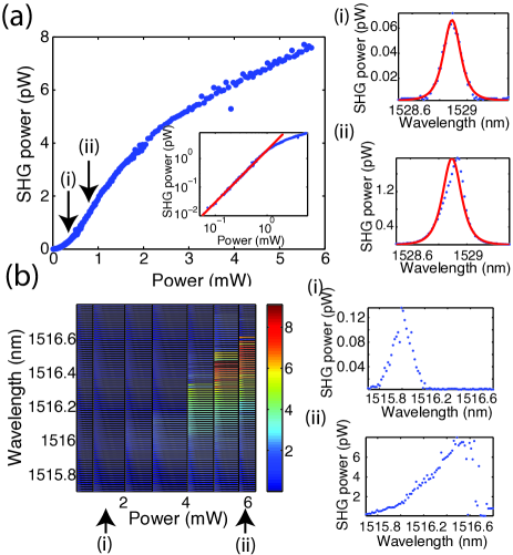
At higher input pump powers, the generated second harmonic will deviate from a quadratic dependence due to absorption processes and resonance shifts. This is shown in Fig. 2 (a). The fundamental is absorbed via two photon absorption, while the second harmonic is absorbed linearly. This absorption leads to the generation of free carriers and free carrier absorption. Additionally, free carrier absorption causes a change in refractive index causing the cavity to blueshift Bennett, Soref, and del Alamo (1990), as well as heating of the cavity, causing the cavity to redshift (microsecond timescale). These transient effects cause regenerative oscillations or bistability, particularly on the red side of the resonance Gibbs (1985); Van et al. (2002); Xu and Lipson (2006), and are of interest for switching and optical signal processing applications Almeida et al. (2004); Nozaki et al. (2010); Fan et al. (2012); buc . In addition, photo-oxidation of the cavity causes a slow and permanent blueshift of the cavity resonance by up to several nm Lee et al. (2009). The input powers at which this deviation from quadratic behavior occurs varied significantly from cavity to cavity. The described resonance shifts can cause problems during measurement, as high Q cavities shift off resonance suddenly. Fig. 2 (a) parts (i) and (ii) show the second harmonic spectrum at low and higher power; at higher powers the spectrum can be seen to be slightly ‘tilted’ from the Lorentzian squared fit due to nonlinear absorption effects. Fig. 2 (b) shows the second harmonic power versus wavelength versus input power for another cavity with higher absorption. As the power is increased, the spectrum deviates more and more from a Lorentzian squared. This is shown in parts (i) and (ii) where the spectra are shown at the low and high power ends. The high power spectrum is highly asymmetric and the peak has redshifted; the second harmonic also becomes bistable at this side of the spectrum (see supplement).
In summary, we have demonstrated second harmonic generation in (111) GaAs
with the pump at telecommunications wavelengths. We observed higher
conversion efficiencies for the (111) GaAs than in (001) GaAs, which is most
likely due to the combination of reduced two photon absorption for TE-like
modes relative to (001) GaAs, and better overlap between involved (TE-like)
modes. Future experiments at longer pump wavelengths could assert which
effects are
more responsible for this difference.
This work was supported by the National Science Foundation (NSF Grant ECCS-
10 25811), a National Science Graduate Fellowship, and Stanford Graduate
Fellowships. This work was performed in part at the Stanford
Nanofabrication Facility of NNIN supported by the National Science
Foundation under Grant No. ECS-9731293, and at the Stanford Nano Center. JV
also thanks the Alexander von Humboldt Foundation for support.
Supplementary Information
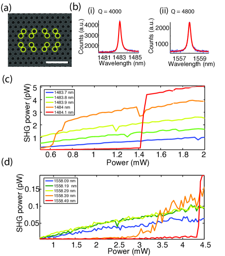
To more easily characterize the bistable behavior of the cavities, we fabricated perturbed L3 cavities in both (001) and (111) oriented wafers. An SEM of a perturbed cavity is shown in Fig. 3 (a), the perturbation is an increase in the radius of specific holes in the cavity region indicated by the yellow circles. Incoupling is improved in these cavities by folding back Fourier components outside the light cone to k = 0 using a perturbation of period , where is the lattice constant. This degrades the Q factor; the cavities we measured had Q factors of 3,000-6,000. Fig. 3 (b) shows cross-polarized reflectivity spectra for cavities in (i) (111) GaAs and (ii) (001) GaAs, with Q factors of 4000 and 4800 respectively. The bistable behaviour was more easily characterized in these cavities. Fig. 3 shows the SHG power versus input power at different wavelengths for a typical perturbed cavity in (c) (111) GaAs and (d) (001) GaAs. These are taken at a power level where the dependence on power is no longer quadratic. The curves shown on the blue side of the resonance are continuous, while the curves on the red side of the resonance have a sudden jump in output power; this jump corresponds to the onset of bistability in the structure. Oscillations will occur at these wavelengths until photo-oxidation blueshifts the resonance far enough and the power becomes unrecoverable. This happens as the cavity heats up and the resonance redshifts and comes into resonance with the laser wavelength. We note that the (001) cavity has lower counts than the (111) cavity at all powers, which was typically the case.
References
- Rodriguez et al. (2007) A. Rodriguez, M. Soljačić, J. D. Joannopoulos, and S. G. Johnson, Optics Express 15, 7303 (2007).
- Eyres et al. (2001) L. A. Eyres, P. J. Tourreau, T. J. Pinguet, C. B. Ebert, J. S. Harris, M. M. Fejer, L. Becouarn, B. Gerard, and E. Lallier, Applied Physics Letters 79, 904 (2001).
- Rivoire et al. (2011) K. Rivoire, S. Buckley, A. Majumdar, H. Kim, P. Petroff, and J. Vučković, Applied Physics Letters 98, 083105 (2011).
- Buckley et al. (2012) S. Buckley, K. Rivoire, F. Hatami, and J. Vučković, Applied Physics Letters 101, 161116 (2012).
- Ota et al. (2013) Y. Ota, K. Watanabe, S. Iwamoto, and Y. Arakawa, Optics Express 21, 19778 (2013).
- Kuo and Solomon (2012) P. S. Kuo and G. S. Solomon, arXiv:1210.1984 (2012).
- Levy et al. (2011) J. S. Levy, M. A. Foster, A. L. Gaeta, and M. Lipson, Optics Express 19, 11415 (2011).
- McCutcheon et al. (2007) M. W. McCutcheon, J. F. Young, G. W. Rieger, D. Dalacu, S. Frédérick, P. J. Poole, and R. L. Williams, Physical Review B 76, 245104 (2007).
- Rivoire et al. (2009) K. Rivoire, Z. Lin, F. Hatami, W. T. Masselink, and J. Vučković, Optics Express 17, 22609 (2009).
- Diziain et al. (2013) S. Diziain, R. Geiss, M. Zilk, F. Schrempel, E.-B. Kley, A. Tünnermann, and T. Pertsch, Applied Physics Letters 103, 051117 (2013).
- Ilchenko et al. (2003) V. S. Ilchenko, A. B. Matsko, A. A. Savchenkov, and L. Maleki, Journal of the Optical Society of America B 20, 1304 (2003).
- Fürst et al. (2010) J. U. Fürst, D. V. Strekalov, D. Elser, M. Lassen, U. L. Andersen, C. Marquardt, and G. Leuchs, Physical Review Letters 104, 153901 (2010).
- Förtsch et al. (2013) M. Förtsch, J. U. Fürst, C. Wittmann, D. Strekalov, A. Aiello, M. V. Chekhova, C. Silberhorn, G. Leuchs, and C. Marquardt, Nature Communications 4, 1818 (2013).
- Liscidini and Andreani (2004) M. Liscidini and L. C. Andreani, Applied Physics Letters 85, 1883 (2004).
- Zhang et al. (2009) Y. Zhang, M. W. McCutcheon, I. B. Burgess, and M. Lončar, Optics Letters 34, 2694 (2009).
- Burgess et al. (2009) I. B. Burgess, Y. Zhang, M. W. McCutcheon, A. W. Rodriguez, J. Bravo-Abad, S. G. Johnson, and M. Loncar, Optics Express 17, 20099 (2009).
- Thon et al. (2010) S. M. Thon, W. T. M. Irvine, D. Kleckner, and D. Bouwmeester, Physical Review Letters 104, 243901 (2010).
- Rivoire, Buckley, and Vučković (2011a) K. Rivoire, S. Buckley, and J. Vučković, Optics Express 19, 22198 (2011a).
- Rivoire, Buckley, and Vučković (2011b) K. Rivoire, S. Buckley, and J. Vučković, Applied Physics Letters 99, 013114 (2011b).
- Joannopoulos et al. (2011) J. D. Joannopoulos, S. G. Johnson, J. N. Winn, and R. D. Meade, Photonic Crystals: Molding the Flow of Light (Second Edition) (Princeton University Press, Princeton, 2011).
- Takayama et al. (2005) S.-i. Takayama, H. Kitagawa, Y. Tanaka, T. Asano, and S. Noda, Applied Physics Letters 87, 061107 (2005).
- McCutcheon et al. (2011) M. W. McCutcheon, P. B. Deotare, Y. Zhang, and M. Lončar, Applied Physics Letters 98, 111117 (2011).
- Dvorak et al. (1994) M. Dvorak, W. Schroeder, D. Andersen, A. L. Smirl, and B. Wherrett, IEEE Journal of Quantum Electronics 30, 256 (1994).
- Altug and Vuckovic (2005) H. Altug and J. Vuckovic, Optics Express 13, 8819 (2005).
- Shoji et al. (1997) I. Shoji, T. Kondo, A. Kitamoto, M. Shirane, and R. Ito, Journal of the Optical Society of America B 14, 2268 (1997).
- (26) See supplementary material at [URL will be inserted by APL] for information on measurements of second harmonic generation in perturbed L3 photonic crystal cavities.
- Bennett, Soref, and del Alamo (1990) B. Bennett, R. A. Soref, and J. del Alamo, IEEE Journal of Quantum Electronics 26, 113 (1990).
- Gibbs (1985) H. M. Gibbs, in Optical Bistability: Controlling Light with Light (Academic Press, 1985) pp. 241–303.
- Van et al. (2002) V. Van, T. Ibrahim, P. Absil, F. Johnson, R. Grover, and P.-T. Ho, IEEE Journal of Selected Topics in Quantum Electronics 8, 705 (2002).
- Xu and Lipson (2006) Q. Xu and M. Lipson, Optics Letters 31, 341 (2006).
- Almeida et al. (2004) V. R. Almeida, C. A. Barrios, R. R. Panepucci, and M. Lipson, Nature 431, 1081 (2004).
- Nozaki et al. (2010) K. Nozaki, T. Tanabe, A. Shinya, S. Matsuo, T. Sato, H. Taniyama, and M. Notomi, Nature Photonics 4, 477 (2010).
- Fan et al. (2012) L. Fan, J. Wang, L. T. Varghese, H. Shen, B. Niu, Y. Xuan, A. M. Weiner, and M. Qi, Science 335, 447 (2012), PMID: 22194410.
- Lee et al. (2009) H. S. Lee, S. Kiravittaya, S. Kumar, J. D. Plumhof, L. Balet, L. H. Li, M. Francardi, A. Gerardino, A. Fiore, A. Rastelli, and O. G. Schmidt, Applied Physics Letters 95, 191109 (2009).