Fano Interference between a STM Tip and Mid Gap States in Graphene
Abstract
We analyze the STM current through electronic resonances on a substrate as a function of tip-surface distance. We show that when the tip approaches the surface a Fano hybridization can occur between the electronic resonance on the substrate and the continuum of conduction states in the STM tip. A maximum of the density of states of the electronic resonance at some energy can then lead to a dip of the STM signal . Resonances in graphene, known as mid gap states, are good candidates to produce this type of Fano interference. The mid gap states can be produced by local defects or adsorbates and we analyze the cases of top and hollow configurations of adsorbates.
pacs:
72.80.Vp; 74.55.+v; 73.63.-bIntroduction The Scanning Tunneling Microscope (STM) is of major importance in the investigation of local structural and electronic properties of surfaces or nano-objects. In particular resonances such as localized states in a nanostructure or near a defect, or atomic and molecular resonances can well be studied by this technique. Yet a proper interpretation of the STM signal in these cases requires a detailed theoretical analysis due in particular to the complex Fano hybridization effects that can occur Fano ; Andrey ; Plihal ; Madhavan ; Balatsky ; Zawadowski .
When the STM is used in the far distance mode the signal in proportional to the density of states (DOS) on the substrate close to the STM tip Tersoff and the STM signal in the presence of a narrow resonance can present a complex Fano-like behaviorFano ; Andrey ; Plihal ; Madhavan ; Balatsky ; Zawadowski . This reflects the combined effect of the coupling of the tip with the different states on the substrate and of the hybridization between the localized resonant state on the substrate and the extended conduction states that are also on the substrate. For example, on a metal, the coupling of the tip with the conduction states can be the dominant term in which case the Kondo resonance can lead to a dip of the signal dI/dV Zawadowski . For graphene, due to the low density of conduction states near the Dirac energy, the coupling with the localized atomic orbital can be essential. In that case the measured STM signal dI/dV can present a resonance similar to the density of states on the localized orbital Neto ; wehling .
Yet the STM can also be used in a near contact regime in which case the coupling between the tip and the substrate is not small. This may modify the electronic structure of the resonance and increase its width due to the coupling with the continuum of states of the STM tip Plihal . In the case of a magnetic atom this coupling can even affect the magnetic moment carried by the orbitalNeto . In addition the standard Tersoff and Hamann theory Tersoff which assumes that the current is due to a weak tunneling process between the tip and the substrate is no more valid. In fact even without a resonance the proximity of the tip with the substrate can deeply modify the STM signal Ferrer ; Hofer ; Blanco ; Ryan . For example it has been shown perez that depending on the tip surface distance the bright spot in the image of graphene can represents either the carbon atoms (far distance) or the centers of the hexagons (short distances). For a resonance on a metallic surface this effect has been theoretically analyzed Plihal in the case of a Kondo impurity but in the case of graphene this regime has not been considered so far.
In this article we analyze theoretically the STM current through a resonant state on a substrate and consider the case where the tip-surface varies from a far distance to a near contact regime. A simple formalism, based on a one channel Landauer model, shows that for small tip-surface distance the perturbative theory of the STM signal is not valid and the STM image does not represent the local density of states. We find that the high local density of states due to the resonant state, can lead to a dip (anti-resonance) for the differential conductance . This is due to a Fano hybridization between the electronic resonance on the substrate and the conduction states of the STM tip. Resonances in graphene, known as mid gap states, are good candidates to produce this type of Fano interference. The mid gap states can be produced by local defects or adsorbates and we analyze the cases of top and hollow configurations of adsorbates.
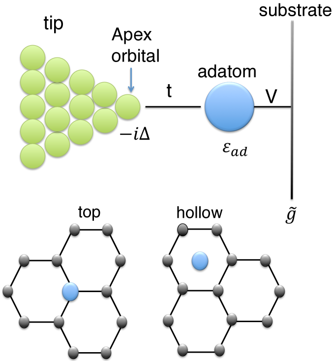
Formalism We discuss now the approximations and the formalism used to compute the differential conductance. We consider a simplified model for the tip and assume that the current flows between the tip and the substrate only through one orbital of the tip, that we name the apex orbital (AO). This implies that the problem of transport can be mapped onto a one channel model as shown for example in Darancet . We define the central part of the circuit as the AO, the left lead is constituted by the rest of the STM tip and the right lead is constituted by the zone of the electronic resonance and the rest of the substrate (see figure 1). Sufficiently far from the apex of the tip and from the zone of the electronic resonance in the substrate the system is assumed to be ballistic. We thus consider the formalism developed in Darancet which allows to consider the case where the leads are ballistic sufficiently far from the central part of the device but can be non ballistic near the central part of the device. In the one channel case the theory Darancet leads to the formula:
| (1) |
where and are injection rates for the STM (left) and substrate (right) lead. is the diagonal element of Green’s function on the central part of the device which here is simply the apex orbital. The on-site energy of the AO is taken as the energy origin and set to zero and is given by :
| (2) |
where and are the self-energy of the state coupled respectively to the rest of the tip and to the substrate. The expression of and (equation (7) of reference Darancet ) is in general (multi-channel case) different from that of the corresponding terms in the standard Fisher-Lee formula. Yet there is a simplification in the one channel case that was not noted in reference Darancet . As we show now the formula (1) is equivalent to the standard Fisher-Lee formula for the one channel case.
Let us consider the apex orbital (AO) and the right lead (side of the substrate). According to Darancet this system can be mapped on a one dimensional chain of orbitals where is an integer. represents the AO orbital and represent all other orbitals of the lead which are states in the substrate. The one dimensional chain has an Hamiltonian given by orbitals on-site energies and coupling between successive orbitals and which is . One defines the restricted Green’s function for site as:
| (3) |
is the on-site Green’s function on site when all sites are removed. Using the above equation (3) one finds that:
| (4) |
where is the imaginary part of complex number . One can assume that and tend to asymptotic values at large . Therefore we set and for . This means that the effective one dimensional lead is ballistic after some level with as discussed in reference Darancet . is given by equation (7) of reference Darancet ) in term of the propagator in the lead and of the standard . Using standard formulas with projectors introduced by Zwanzig and Mori (equation B(12) of Darancet ) we arrive at the expression :
| (5) |
Then it is straightforward to show that for a one channel model and . The generalized Fisher-Lee formula (equation (1)) derived in Darancet can therefore be written :
| (6) |
Thus even if the propagation in the tip and in the substrate is not ballistic locally in the vicinity of the apex orbital the Fisher-Lee formula (which assumes that the propagation is everywhere ballistic up to the apex orbital) still applies. Let us emphasize that it is specific to the one channel model which is applicable here because the current is assumed to pass entirely through one orbital i.e. the apex orbital. As shown by equation (6) a good model of self-energies for the apex orbital gives enough information for computing current through the STM. We exploit this now to analyze some general aspects of Fano interference in the case of resonances.
Conditions for the Occurrence of Fano Interferences We model the self-energy due to the coupling of the AO with the tip by . Here is the width of the resonance of the DOS of the apex orbital of the STM tip alone. For simplicity we consider the case where the electronic resonant state is an orbital of an adsorbate atom, but the conclusions are more general as it will appear. We note the coupling between the AO and the adsorbate orbital AD. We note the dimensionless quantity . In this work we shall take eV and eV. One has therefore where is the green’s function of the adatom orbital coupled to the substrate alone i.e. without coupling to the STM tip.
| (7) |
where is the on-site energy of the orbital. is the self-energy of the adsorbate orbital due to its coupling with the substrate. Note that, due to their analytical properties, self-energies can always be written under the form of the equation ( 7). Therefore the conclusions drawn below are applicable to other resonant states and are not specific to adsorbates. For the present model the equation (6) leads to the expression:
| (8) |
where is the density of states on the orbital of the adsorbate without coupling to the STM tip.
When the hopping integral tends to zero, i.e. when the STM tip is at a sufficiently large distance of the surface, (). Then, assuming that the energy is within the resonance of the STM tip (i.e. ) one get from equation ( 8) . The transmission is proportional to the local density of states close to the apex of the tip in agreement with the standard Tersoff-Hamann theory.
Let us examine the effect of the term in equation (8). In order that this term play a role its modulus must be at least of the order of . This condition () can be attained. Indeed for energies close to the resonance we have where is the width of the resonance. can be satisfied if where the critical valuet is :
| (9) |
Note that the transmission in this regime is necessarily small. Indeed is the imaginary part of therefore , so that after equation (8) the transmission is . For and for energies such that equation (6) leads to:
| (10) |
can be written as where is the coupling between the orbital of the adsorbate and the substrate. is the green’s function of the states of the substrate which are coupled to the adsorbate orbital. Equation (10) means that the variation with energy of the transmission depends only on the effective DOS of the substrate . In the case of graphene the effective DOS presents a dip close to zero energy. Therefore the we expect that the STM signal can present a dip instead of a resonance. This is confirmed by the model calculation as shown below.
According to formula ( 10) the STM tip probes the effective DOS of the states of the substrate that are coupled to the tip (via the adsorbate). In fact the adatom is sufficiently coupled to the STM tip that it can be considered as the apex atom of the STM tip. Finally let us emphasize that in this regime the transmission is not proportional to the DOS on the adsorbate only coupled to the substrate after equation (8). is also not proportional to the DOS on the adsorbate coupled to the tip and to the substrate, which value is .
We analyze now some models. The calculation neglects the possibility of collective effects like the Kondo resonance and therefore applies to temperature greater than the Kondo temperature. In addition we do not treat the possible existence of localized magnetic moment on the adsorbate. This means that the present calculation concerns only one type of spin, and in a true system with localized magnetic moment on the adsorbate the two contributions of the two spins (majority and minority) should be added Anderson ; Neto . The first two models concern an adsorbate on graphene either in a top position or in a hollow position. For comparison we also consider a model of an adsorbate on a metallic substrate. All the effect of the substrate is contained in the quantity which is known for the three models.
Adatom in top position on graphene In this configuration the adatom is right above one carbon atom of the graphene layer as shown in figure(1). The self-energy is given by :
| (11) |
 |
 |
is a high-energy cutoff of order of the graphene bandwidth. eV where eV is the hoping energy between nearest neighbors sites of graphene. is the hybridization amplitude of the orbital of the adatom with the orbital of the nearest carbon atom Neto . Here we consider typical parameters for an hydrogen atom and then eV.
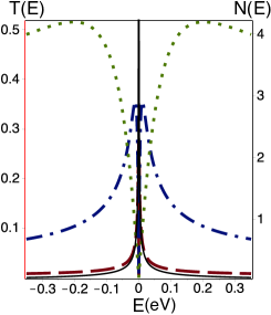
Figure 2 represents the density of states on the adatom orbital and the transmission for two values of the on-site energy of the adatom orbital eV and eV . In both cases the density of states of the adsorbate on the substrate presents a peak at an energy close to the on-site energy . In the symmetric case the peak of the density of states is precisely at the on-site energy eV. In the non symmetric case there is a small shift between the position of the peak and eV, due to repulsion of level by coupling with the continuum of graphene states.
The transmission is shown in figure 2 for the two on-site energies and different values of . For small the transmission varies in accordance with the density of states on the adsorbate as expected from the Tersoff-Hamann theory. For larger the peak of the density is preserved in the transmission but there is some distortion and is not strictly proportional to . For the transmission differs completely from . In fact close to the energy of the resonance the coupling between the resonant state on the graphene side and the conduction state on the tip induce a Fano interference. In this regime and the formula (10) is valid. Indeed the transmission varies like the imaginary part of as given by equation (11). In this regime reflects the DOS of the substrate as discussed above.
Adatom in hollow position on graphene In this configuration the adatom is right above the center of an hexagon of the graphene layer, as shown in figure(1). The self-energy is given by Neto
| (12) |
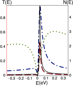
where , and eV have the same values as for the case of top position. is the coupling of the orbital of the adatom with the orbitals of each of the nearest neighbors carbon atoms. It is important to notice that the imaginary part in Equation Fano Interference between a STM Tip and Mid Gap States in Graphene is much smaller, at low energy , than for Equation 11 i.e ( ). This is due to interferences effect in the coupling between the orbital of the adatom and the orbitals of the six neighbors carbon atoms in the hollow geometry. This means that an adsorbate in the hollow position is less coupled to low energy states of graphene than in the top position. This will favor narrower resonance with higher density of states, as shown below.
 |
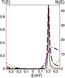 |
Figure 3 represents the density of states of the adsorbate and the transmission for eV and eV . In both cases presents a peak at an energy close to the on-site energy . Note that for is a singular case. Indeed presents a delta peak at with a weight . This delta peak is made apparent in Figure 3 due to a small finite imaginary part of , eV. In the non symmetric case, eV, the shift between the position of the peak and is smaller than for the top configuration. This is due to the smaller coupling to graphene states and therefore to a smaller level repulsion effect.
The transmission is shown in figure 3 for the two values of and different . The conclusions are qualitatively similar to those for the top configuration. For small the transmission varies in accordance with the density of states on the adsorbate as expected from the Tersoff-Hamann theory. For larger the peak of the density is preserved in the transmission but there is a strong distortion and is not proportional to . For differs completely from . For this case the coupling between the resonant state on the graphene side and the conduction state on the tip induce a Fano interference. Again in this regime and the formula (10) is valid. The transmission varies like the imaginary part of as given by equation (11). In this regime reflects the DOS of the states of the substrate which are coupled to the adsorbate, as discussed above.
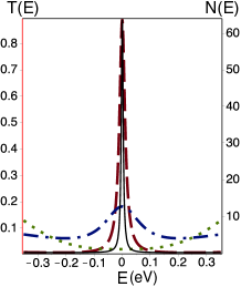
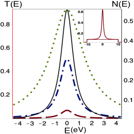
Adatom on a metallic substrate— For comparison we consider a third model that is for an adsorbate on a metallic substrate. We keep the same value of the coupling orbital eV and we have chosen a rectangular band-model for . In the present calculations we take eV which is a typical value for a metal. The self-energy is:
| (13) |
In that case the width of the electronic resonance is greater because the density of states of the metallic substrate is higher than that of graphene close to the Dirac energy . Therefore the condition cannot be achieved for the same values of and as before, and the Fano interference plays a minor role. As shown in Figure 4 the DOS of the adatom presents a wide resonance on a metallic substrate because the density of state of the metallic substrate is larger than for graphene (top or hollow). As a consequence the phenomena of anomalous STM image does not occur because the resonance is too large to reach to regime . Yet this model shows that the characteristics of a resonance on a metallic substrate like its width can be sensitive to the coupling with the tip in a way that cannot be described by the Tersoff-Hamann approach.
Conclusion
To conclude the present work shows that the mid gap states in graphene, which have received much attention due to their peculiar electronic structure and scattering properties lead not only to special transport properties Mayou but also to special response to STM measurements. We propose a physical mechanism in which a Fano interference occurs between an electronic resonance on a substrate and the conduction states of a STM tip. This Fano effect occurs typically if the coupling between the tip and the resonant state satisfies where and are the width of the STM resonance and the width of the electronic resonance on the substrate. Therefore the occurence of this Fano effect is favored for resonances of narrow width . We expect that this mechanism is rather general but we analyzed specifically two models for resonance on an adsorbate on graphene. These narrow resonances, which are favored by the low density of states in graphene, have been studied for realistic parameters of the coupling between the adsorbate and the substrate. We find that the effect should be observable and is stronger for the hollow position than for the top position. This is because in the hollow position the resonance is more pronounced. Other mid gap states exist in graphene, that are produced for example by vacancies, and they should lead to similar effects. Finally we note that Fano effect have been well identified in the context of electronic properties of alloys when the hybridization between localized d orbitals and extended sp orbitals is strong Mayou2 ; Nguyen ; Pasturel .
References
- (1) U. Fano Phys. Rev. 124, 1866 (1961)
- (2) Andrey E. Miroshnichenko, Sergej Flach, Yuri S. Kivshar; Rev. Mod. Phys. 82, 2257-2298 (2010)
- (3) M. Plihal and J. W. Gadzuk; Phys. Rev. B 63, 085404 (2001)
- (4) V. Madhavan, W. Chen, T. Jamneala, M. F. Crommie and Ned S. Wingreen ; Phys. Rev. B 64, 165412 (2001)
- (5) Jian-Xin Zhu1, Jean-Pierre Julien, Y. Dubi and A. V. Balatsky; Phys. Rev. Lett. 108, 186401 (2012)
- (6) O. Újsághy, J. Kroha, L. Szunyogh, and A. Zawadowski; Phys. Rev. Lett. 85, 2557 (2000)
- (7) J. Tersoff and D. R. Hamann ; Phys. Rev. B 31, 805 (1985)
- (8) Bruno Uchoa, Ling Yang, S.-W. Tsai, N. M. R. Peres, and A. H. Castro Neto; Phys. Rev. Lett. 103, 206804 (2009)
- (9) T. O. Wehling, H. P. Dahal, A. I. Lichtenstein, M. I. Katsnelson, H. C. Manoharan4, and A. V. Balatsky; Phys. Rev. B 81, 085413 (2010)
- (10) J. Ferrer, A. Martin-Rodero, and F. Flores Phys. Rev. B 38, 10113 (1988)
- (11) Werner A. Hofer, Adam S. Foster and Alexander L. Shluger; Rev. Mod. Phys. 75, 1287-1331 (2003)
- (12) Blanco, Jose Manuel and Flores, Fernando and Pérez, Rubń; Progress in Surface Science, Volume 81, Issue 10-12, p. 403-443 (2006)
- (13) Ryan, P. M., Teague, L. C. , Naydenov B., Borland D. and Boland, John J ; Phys. Rev. Lett. 101, 096801 (2008)
- (14) Martin Ondráček, Pablo Pou, Vít Rozsíval, Cesar González, Pavel Jelínek, and Rubén Pérez; Phys. Rev. Lett. 106, 176101 (2011)
- (15) Datta, S., Electronic Transport in Mesoscopic Systems (Cambridge University Press, Cambridge), 1995.
- (16) Pierre Darancet, Valerio Olevano, Didier Mayou; Phys Rev B 81, 155422 (2010)
- (17) P.W. Anderson Phys. Rev. 124, 41 (1961)
- (18) Guy Trambly de Laissardière and Didier Mayou; Phys. Rev. Lett. 111, 146601 (2013)
- (19) D. Mayou, D. Nguyen-Manh, A. Pasturel, and F. Cyrot-Lackmann Phys. Rev. B 33, 3384 (1986)
- (20) D Nguyen-Manh, D Mayou, G J Morgan and A Pasturel; J. Phys. F: Met. Phys. 17, 999 (1987)
- (21) A. Pasturel, D.Nguyen Manh, D. Mayou; Journal of Physics and Chemistry of Solids 47, 325 (1986)